Downloaded 5,026 times


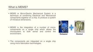
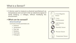

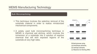
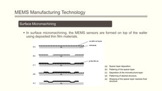


MEMS (Micro-Electro-Mechanical Systems) integrates electrical and mechanical components on a chip for miniature systems that sense and control environments. It utilizes various sensors and fabrication methods, including micromachining techniques, to produce high-quality, cost-effective devices applicable in fields like medical and marine science. The conclusion emphasizes that MEMS can facilitate a connected and proactive computing environment, enhancing real-time data acquisition and productivity.


![Getting Started with Apache Spark: Big Data Made Simple [Free Meetup]](https://cdn.slidesharecdn.com/ss_thumbnails/apachesparkgettingstarted-260203175547-8361bcc3-thumbnail.jpg?width=640&height=640&fit=bounds)


