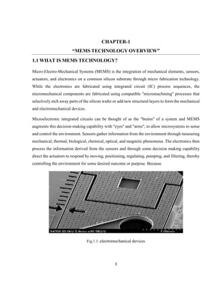
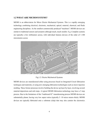
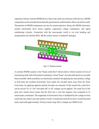
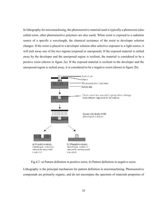
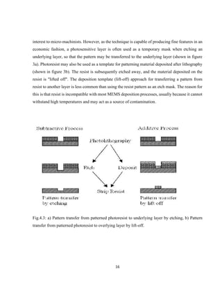
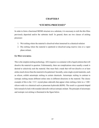
SlideShare a Scribd company logo
i
A
SEMINAR REPORT
ON
“MEMS TECHNOLOGY”
Submitted by
RIYAJ MIRZA
In partial fulfillment for the award of the degree
Of
BACHELOR OF TECHNOLOGY
(RAJASTHAN TECHNICAL UNIVERSITY, KOTA)
IN
ELECTRONICS AND COMMUNICATION ENGINEERING
UNDER THE GUIDANCE OF
PROF. HEENA JOSHI
AT
JODHPUR INSTITUTE OF ENGINEERING AND TECHNOLOGY
MOGRA, N.H. 65, PALI ROAD,
JODHPUR-342802
MARCH&2016
ii
Candidate’s Declaration
I hereby declare that the work, which is being presented in the Seminar, entitled “MEMS
TECHNOLOGY” in partial fulfillment for the award of Degree of “Bachelor of
Technology” in Dept Of Electronics & communication Engineering with Specialization
in Electronics and communication and submitted to the Department of Electronics
and Communication Engineering, Jodhpur Institute of Engineering and
Technology, Rajasthan Technical University is a record of my own WORK carried
under the Guidance of Prof.HEENA JOSHI Department of Electronics and
Communication Engineering, Jodhpur Institute of Engineering and Technology .
I have not submitted the matter presented in this Seminar anywhere for the award of any
other Degree.
NAME-RIYAJ MIRZA
Enrolment No.:12EJIEC096
Counter Signed by
Name of Guide Name of Incharge
PROF.HEENA JOSHI PROF.SHWETA BHATI
iii
ACKNOWLEDGEMENT
We deeply express our sincere thanks to our Head of seminar coordinator Prof.
SHWETA BHATI for encouraging and allowing us to present the project on the topic
“MEMS TECHNOLOGY”.
We would like to make a number of acknowledgements to those who have helped us to
prepare this Seminar.
We are highly grateful to Prof. O. P. VYAS, Dean (Engineering), JIET for proving us
this opportunity to carry out independent study on this topic.
The divine support given by our guide Prof. HEENA JOSHI and Prof. K. K. ARORA,
HOD (M. Tech) & Prof. (Dr.) HEMANT PUROHIT, HOD (B. Tech) Department of
Electronics and Communication Engineering, J.I.E.T, Jodhpur, without them the work
would not be possible.
We take this opportunity to thank all ours teacher who have directly or indirectly helped
our project. We pay our respects and love to our parents and all other family members
and friends for their love and encouragement throughout our career. Last but not the least
we express our thanks to our friends for their cooperation and support.
NAME:-RIYAJ MIRZA
ROLL NO:-12EJIEC096
iv
ABSTRACT
Micromechanical systems can be combined with microelectronics, photonics or wireless
capabilities new generation of Microsystems can be developed which will offer far
reaching efficiency regarding space, accuracy, precision and so forth. Micromechanical
systems (MEMS) technology can be used fabricate both application specific device.
The associated micro packaging systems that will allow for the integration of devices or
circuits, made with non-compatible technologies, with a System-on-Chip environment.
The MEMS technology can be used for permanent, semipermanent or temporary
interconnection of sub modules in a System-on-Chip implementation. The
interconnection of devices using MEMS technology is described with the help of a
hearing instrument application and related.
MEMS technology has enabled us to realize advanced micro devices by using processes
similar to VLSI technology. When MEMS devices are combined with other technologies
new generation of innovative technology will created. This will offer outstanding
Functionality. Such technologies will have wide scale applications in fields ranging from
automotive, aerodynamics, and hydrodynamics, biomedical and so forth. The main
challenge is to integrate all these potentially non-compatible technologies into a single
working Microsystem that will offer outstanding functionality.
v
TABLE OF FIGURE
FIGURE FIGURE NAME PAGE NO.
NO.
Chapter -1
1.1 Electromechanical device 3
1.2 Electromechanical system 4
1.3 Surface mount 5
Chapter -2
2.1 Hot wall LPCVD reactor 7
2.2 Setup of electro deposition 9
2.3 Cold wall vapor phase epitaxial reactor 10
Chapter -3
3.1 System for e-beam evaporation material 12
3.2 RF sputtering system 13
3.3 Spin casting process used for photo resist 13
Chapter-4
4.1 Transfer of a pattern 14
4.2 Pattern definition of positive & -ve resist 15
4.3 Pattern transfer under layering by etching 16
Chapter-5
5.1 Difference b/w anisotropic & Isotropic 18
Chapter-7
7.1 IPod Touch 21
7.2 Inertial sensor 22
vi
TABLE OF CONTENTS
Title Page i
Candidate’s Declaration ii
Acknowledgement iii
Abstract iv
List of Figures v
List of Tables vi
Introduction ________________________________________________________1
Literature survey____________________________________________________2
CHAPTERS
1. MEMS TECHNOLOGY OVERVIEW_______________________________3
1.1 What is MEMS technology _______________________________________3
1.2 What are microsystem ___________________________________________4
1.3 Silicon_______________________________________________________6
1.4 Polymers_____________________________________________________6
1.5 Metals_______________________________________________________6
2. CHEMICAL VAPOR DEPOSITION________________________________7
2.1 Introduction__________________________________________________7
2.2 When do want to use CVD ? ____________________________________8
2.3 Electro Deposition_____________________________________________8
2.4 Use Electro Deposition _________________________________________8
2.5 Epitaxy______________________________________________________9
2.6 Thermal Oxidation____________________________________________10
3. PHYSICAL VAPOR DEPOSITION ________________________________11
3.1 When do we want to use PVD____________________________________11
3.2 Evaporation__________________________________________________11
3.3 Sputtering____________________________________________________12
3.4 When do we want to use casting ?_________________________________13
4. PATTERN TRANSFER____________________________________________14
4.1 Introduction___________________________________________________14
5. ETCHING PROCESS______________________________________________17
5.1 Wet Etching___________________________________________________17
5.2 When do we want to use Wet Etching ? _____________________________18
vii
6. FABRICATION TECHNOLOGIES__________________________________19
6.1 Introduction___________________________________________________19
6.2 IC Fabrication_________________________________________________20
7. APPLICATION___________________________________________________21
7.1 Pressure Sensors_______________________________________________21
7.2 Accelerometers ________________________________________________21
7.3 Inertial Sensor _________________________________________________22
8. ADVANTAGE & DISADVANTAGE OF MEMS________________________23
8.1 Advantage of MEMS_____________________________________________23
8.2 Disadvantage of MEMS___________________________________________23
CONCLUSION______________________________________________________24
REFERENCE________________________________________________________25
APPENDIX_________________________________________________________26
1
INTRODUCTION
Micro electromechanical systems (MEMS) are small integrated devices or systems that combine
electrical and mechanical components. They range in size from the sub micro meter level to the
milli meter level and there can be any number, from a few to millions, in a particular system.
MEMS extend the fabrication techniques developed for the integrated circuit industry to add
mechanical elements such as beams, gears, diaphragms, and springs to devices.
Examples of MEMS device applications include inkjet-printer cartridges, accelerometer, miniature
robots, micro engines, locks inertial sensors micro transmissions, micro mirrors, micro actuator
(Mechanisms for activating process control equipment by use of pneumatic, hydraulic, or
electronic signals) optical scanners, fluid pumps, transducer, pressure and flow sensors. New
applications are emerging as the existing technology is applied to the miniaturization and
integration of conventional devices.
These systems can sense, control, and activate mechanical processes on the micro scale, and
function individually or in arrays to generate effects on the macro scale. The micro fabrication
technology enables fabrication of large arrays of devices, which individually perform simple tasks,
but in combination can accomplish complicated functions. MEMS are not about any one
application or device, nor are they defined by a single fabrication process or limited to a few
materials. They are a fabrication approach that conveys the advantages of miniaturization, multiple
components, and microelectronics to the design and construction of integrated electromechanical
systems. MEMS are not only about miniaturization of mechanical systems; they are also a new
paradigm for designing mechanical devices and systems. The MEMS industry has an estimated
$10 billion market, and with a projected 10-20% annual growth rate, it is estimated to have a $34
billion market in 2002. Because of the significant impact that MEMS can have on the commercial
2
LITERATURE SURVEY
I. We referred following paper for writing this seminar report,
1. “Implementation of AHB Interface as SDR-SDRAM Controller’s CPU
Interface”, proceedings of 2nd national conference, Sapna Gupta, Arti Noor,
Shruti Sabharwal. INDIACom-2008, BVICAM-2008, Delhi held on 8-9 Feb
2008.
2. Sharma, R., Chakravarty, T., and Bhattacharyya, A. B., “Analytical model for
optimum signal integrity in PCB interconnects using ground tracks”, IEEE
Transactions on Electromagnetic Compatibility, Vol. 51 (1), pp. 67-77,
2009. [[Impact Factor : 1.083, Indexed in SCOPUS]
3. Sharma, R. Chakravarty, T., and Bhattacharyya, A. B., “Transient Analysis of
Microstrip-Like Interconnections Guarded by Ground Tracks,” Progress in
Electromagnetic Research, vol. PIER 82, pp.189-202, 2008.
II. We referred following book writing this seminar report.
1. Chauhan, T. & Bhagabati, C.D. & Kumar, V., 2011. Era of Energy
Harvesting: µ -Energy Scavengers using Microsystems (MEMS) Technology.
2. Shikha Sharma, Nidhi Gupta and Sudha Srivastava “Modulating Electron
Transfer Properties of Gold Nanoparticles for Efficient Biosensing” Current
Nanoscience (communicated).
3. Role of vibrational modes in structural relaxation in a supercooled
liquid”, Shankar P. Das and Sudha Srivastava in “Slow Dynamics in Complex
System” – Edited by Michio Tokuyama and Irwin Oppenheim, 1999 American
Institute of Physics (AIP).
III. We referred following content from Internet
1. Application of MEMS technology
2. Future scope of MEMS technology
3. Advantage and Disadvantage of MEMS/MICRO system
3
CHAPTER-1
“MEMS TECHNOLOGY OVERVIEW”
1.1 WHAT IS MEMS TECHNOLOGY?
Micro-Electro-Mechanical Systems (MEMS) is the integration of mechanical elements, sensors,
actuators, and electronics on a common silicon substrate through micro fabrication technology.
While the electronics are fabricated using integrated circuit (IC) process sequences, the
micromechanical components are fabricated using compatible "micromachining" processes that
selectively etch away parts of the silicon wafer or add new structural layers to form the mechanical
and electromechanical devices.
Microelectronic integrated circuits can be thought of as the "brains" of a system and MEMS
augments this decision-making capability with "eyes" and "arms", to allow microsystems to sense
and control the environment. Sensors gather information from the environment through measuring
mechanical, thermal, biological, chemical, optical, and magnetic phenomena. The electronics then
process the information derived from the sensors and through some decision making capability
direct the actuators to respond by moving, positioning, regulating, pumping, and filtering, thereby
controlling the environment for some desired outcome or purpose. Because
Fig.1.1: electromechanical devices
4
1.2 WHAT ARE MICROSYSTEMS?
MEMS is an abbreviation for Micro Electro Mechanical Systems. This is a rapidly emerging
technology combining electrical, electronic, mechanical, optical, material, chemical, and fluids
engineering disciplines. As the smallest commercially produced "machines", MEMS devices are
similar to traditional sensors and actuators although much, much smaller. E.g. Complete systems
are typically a few millimeters across, with individual features devices of the order of 1-100
micrometers across
Fig.1.2: Electro Mechanical Systems
MEMS devices are manufactured either using processes based on Integrated Circuit fabrication
techniques and materials, or using new emerging fabrication technologies such as micro injection
molding. These former processes involve building the device up layer by layer, involving several
material depositions and etch steps. A typical MEMS fabrication technology may have a 5 step
process. Due to the limitations of this "traditional IC" manufacturing process MEMS devices are
substantially planar, having very low aspect ratios (typically 5 -10 micro meters thick). MEMS
devices are typically fabricated onto a substrate (chip) that may also contain the electronics
5
required to interact with the MEMS device. Due to the small size and mass of the devices, MEMS
components can be actuated electrostatically (piezoelectric and bimetallic effects can also be used).
The position of MEMS components can also be sensed capacitive. Hence the MEMS electronics
include electrostatic drive power supplies, capacitance charge comparators, and signal
conditioning circuitry. Connection with the macroscopic world is via wire bonding and
encapsulation into familiar BGA, MCM, surface mount, or leaded IC packages.
Fig.1.3: Surface mount
A common MEMS actuator is the "linear comb drive" (shown above) which consists of rows of
interlocking teeth; half of the teeth are attached to a fixed "beam", the other half attach to a movable
beam assembly. Both assemblies are electrically insulated. By applying the same polarity voltage
to both parts the resultant electrostatic force repels the movable beam away from the fixed.
Conversely, by applying opposite polarity the parts are attracted. In this manner the comb drive
can be moved "in" or "out" and either DC or AC voltages can be applied. The small size of the
parts (low inertial mass) means that the drive has a very fast response time compared to its
macroscopic counterpart. The magnitude of electrostatic force is multiplied by the voltage or more
commonly the surface area and number of teeth. Commercial comb drives have several thousand
teeth, each tooth approximately 10 micro meters long. Drive voltages are CMOS levels.
6
1.3 SILICON
The economies of scale, ready availability of cheap high-quality materials and ability to
incorporate electronic functionality make silicon attractive for a wide variety of MEMS
applications. Silicon also has significant advantages engendered through its material properties. In
single crystal form, silicon is an almost perfect Hookean material, meaning that when it is flexed
there is virtually no hysteresis and hence almost no energy dissipation. The basic techniques for
producing all silicon based MEMS devices are deposition of material layers, patterning of these
layers by photolithography and then etching to produce the required shapes.
1.4 POLYMERS
Even though the electronics industry provides an economy of scale for the silicon industry,
crystalline silicon is still a complex and relatively expensive material to produce. Polymers on the
other hand can be produced in huge volumes, with a great variety of material characteristics.
MEMS devices can be made from polymers by processes such as injection molding, embossing or
stereo lithography and are especially well suited to microfluidic applications such as disposable
blood testing cartridges.
1.5 METALS
Metals can also be used to create MEMS elements. While metals do not have some of the
advantages displayed by silicon in terms of mechanical properties, when used within their
limitations, metals can exhibit very high degrees of reliability. Metals can be deposited by
electroplating, evaporation, and sputtering processes. Commonly used metals include gold, nickel,
aluminum, chromium, titanium, tungsten, platinum, and silver.
7
CHAPTER-2
‘‘CHEMICAL VAPOR DEPOSITION’’
2.1 INTRODUCTION
In this process, the substrate is placed inside a reactor to which a number of gases are supplied.
The fundamental principle of the process is that a chemical reaction takes place between the source
gases. The product of that reaction is a solid material with condenses on all surfaces inside the
reactor.
The two most important CVD technologies in MEMS are the Low Pressure CVD (LPCVD) and
Plasma Enhanced CVD (PECVD). The LPCVD process produces layers with excellent uniformity
of thickness and material characteristics. The main problems with the process are the high
deposition temperature (higher than 600°C) and the relatively slow deposition rate. The PECVD
process can operate at lower temperatures (down to 300° C) thanks to the extra energy supplied to
the gas molecules by the plasma in the reactor. However, the quality of the films tend to be inferior
to processes running at higher temperatures. Secondly, most PECVD deposition systems can only
deposit the material on one side of the wafers on 1 to 4 wafers at a time. LPCVD systems deposit
Fig.2.1: Typical hot-wall LPCVD reactor.
8
2.2 WHEN DO WE WANT TO USE CVD?
CVD processes are ideal to use when you want a thin film with good step coverage. A variety of
materials can be deposited with this technology; however, some of them are less popular with fabs
because of hazardous by-products formed during processing. The quality of the material varies
from process to process, however a good rule of thumb is that higher process temperature yields a
material with higher quality and less defects.
2.3 ELECTRO DEPOSITION
This process is also known as "electroplating" and is typically restricted to electrically conductive
materials. There are basically two technologies for plating: Electroplating and Electro less plating.
In the electroplating process the substrate is placed in a liquid solution (electrolyte). When an
electrical potential is applied between a conducting area on the substrate and a counter electrode
(usually platinum) in the liquid, a chemical redox process takes place resulting in the formation of
a layer of material on the substrate and usually some gas generation at the counter electrode. In the
electro less plating process a more complex chemical solution is used, in which deposition happens
spontaneously on any surface which forms a sufficiently high electrochemical potential with the
solution. This process is desirable since it does not require any external electrical potential and
contact to the substrate.
2.4 WHEN DO WE WANT TO USE ELECTRO DEPOSITION?
The electro deposition process is well suited to make films of metals such as copper, gold and
nickel. The films can be made in any thickness from ~1µm to >100µm. The deposition is best
controlled when used with an external electrical potential, however, it requires electrical contact
to the substrate when immersed in the liquid bath. In any process, the surface of the substrate must
have an electrically conducting coating before the deposition can be done.
9
Fig.2.2: Typical setup for electro deposition.
2.5 EPITAXY
This technology is quite similar to what happens in CVD processes, however, if the substrate is an
ordered semiconductor crystal (i.e. silicon, gallium arsenide), it is possible with this process to
continue building on the substrate with the same crystallographic orientation with the substrate
acting as a seed for the deposition. If an amorphous/polycrystalline substrate surface is used, the
film will also be amorphous or polycrystalline.
There are several technologies for creating the conditions inside a reactor needed to support
epitaxial growth, of which the most important is Vapor Phase Epitaxy (VPE). In this process, a
number of gases are introduced in an induction heated reactor where only the substrate is heated.
The temperature of the substrate typically must be at least 50% of the melting point of the material
to be deposited.
10
An advantage of epitaxy is the high growth rate of material, which allows the formation of films
with considerable thickness (>100µm). Epitaxy is a widely used technology for producing silicon
on insulator (SOI) substrates. The technology is primarily used for deposition of silicon. A
schematic diagram of a typical vapour phase epitaxial reactor is shown in the figure below.
Fig.2.3: Typical cold-wall vapour phase epitaxial reactor.
2.6 THERMAL OXIDATION
This is one of the most basic deposition technologies. It is simply oxidation of the substrate surface
in an oxygen rich atmosphere. The temperature is raised to 800° C-1100° C to speed up the process.
This is also the only deposition technology which actually consumes some of the substrate as it
proceeds. The growth of the film is spurned by diffusion of oxygen into the substrate, which means
the film growth is actually downwards into the substrate. As the thickness of the oxidized layer
increases, the diffusion of oxygen to the substrate becomes more difficult leading to a parabolic
relationship between film thickness and oxidation time for films thicker than ~100nm. This process
is naturally limited to materials that can be oxidized, and it can only form films that are oxides of
that material.
11
CHAPTER-3
‘‘PHYSICAL VAPOR DEPOSITION’’
PVD covers a number of deposition technologies in which material is released from a source and
transferred to the substrate. The two most important technologies are evaporation and sputtering.
3.1 WHEN DO WE WANT TO USE PVD?
PVD comprises the standard technologies for deposition of metals. It is far more common than
CVD for metals since it can be performed at lower process risk and cheaper in regards to materials
cost. The quality of the films are inferior to CVD, which for metals means higher resistivity and
for insulators more defects and traps. The step coverage is also not as good as CVD. The choice
of deposition method (i.e. evaporation vs. sputtering) may in many cases be arbitrary, and may
depend more on what technology is available for the specific material at the time.
3.2 EVAPORATION
In evaporation the substrate is placed inside a vacuum chamber, in which a block (source) of the
material to be deposited is also located. The source material is then heated to the point where it
starts to boil and evaporate. The vacuum is required to allow the molecules to evaporate freely in
the chamber, and they subsequently condense on all surfaces. This principle is the same for all
evaporation technologies, only the method used to the heat (evaporate) the source material differs.
There are two popular evaporation technologies, which are e-beam evaporation and resistive
evaporation each referring to the heating method. In e-beam evaporation, an electron beam is
aimed at the source material causing local heating and evaporation. In resistive evaporation, a
tungsten boat, containing the source material, is heated electrically with a high current to make the
material evaporate. Many materials are restrictive in terms of what evaporation method can be
used (i.e. aluminium is quite difficult to evaporate using resistive heating), which typically relates
12
to the phase transition properties of that material. A schematic diagram of a typical system for e-
beam evaporation is shown in the figure below.
Fig.3.1: Typical system for e-beam evaporation of materials
3.3 SPUTTERING
Sputtering is a technology in which the material is released from the source at much lower
temperature than evaporation. The substrate is placed in a vacuum chamber with the source
material, named a target, and an inert gas (such as argon) is introduced at low pressure. Gas plasma
is struck using an RF power source, causing the gas to become ionized. The ions are accelerated
towards the surface of the target, causing atoms of the source material to break off from the target
in vapour form and condense on all surfaces including the substrate. As for evaporation, the basic
principle of sputtering is the same for all sputtering technologies. The differences typically relate
to the manner in which the ion bombardment of the target is realized. A schematic diagram of a
typical RF sputtering system is shown in the figure below.
13
Fig.3.2: Typical RF sputtering system.
3.4 WHEN DO WE WANT TO USE CASTING?
Casting is a simple technology which can be used for a variety of materials (mostly polymers).
The control on film thickness depends on exact conditions, but can be sustained within +/-10% in
a wide range. If you are planning to use photolithography you will be using casting, which is an
integral part of that technology. There are also other interesting materials such as polyimide and
spin-on glass which can be applied by casting.
Fig.3.3: The spin casting process as used for photoresist in photolithography
14
CHAPTER-4
“PATTERN TRANSFER”
4.1. INTRODUCTION
Lithography in the MEMS context is typically the transfer of a pattern to a photosensitive material
by selective exposure to a radiation source such as light. A photosensitive material is a material
that experiences a change in its physical properties when exposed to a radiation source. If we
selectively expose a photosensitive material to radiation (e.g. by masking some of the radiation)
the pattern of the radiation on the material is transferred to the material exposed, as the properties
of the exposed and unexposed regions differs (as shown in figure 1).
Fig.4.1: Transfer of a pattern to a photosensitive material.
15
In lithography for micromachining, the photosensitive material used is typically a photoresist (also
called resist, other photosensitive polymers are also used). When resist is exposed to a radiation
source of a specific a wavelength, the chemical resistance of the resist to developer solution
changes. If the resist is placed in a developer solution after selective exposure to a light source, it
will etch away one of the two regions (exposed or unexposed). If the exposed material is etched
away by the developer and the unexposed region is resilient, the material is considered to be a
positive resist (shown in figure 2a). If the exposed material is resilient to the developer and the
unexposed region is etched away, it is considered to be a negative resist (shown in figure 2b).
Fig.4.2 :a) Pattern definition in positive resist, b) Pattern definition in negative resist.
Lithography is the principal mechanism for pattern definition in micromachining. Photosensitive
compounds are primarily organic, and do not encompass the spectrum of materials properties of
16
interest to micro-machinists. However, as the technique is capable of producing fine features in an
economic fashion, a photosensitive layer is often used as a temporary mask when etching an
underlying layer, so that the pattern may be transferred to the underlying layer (shown in figure
3a). Photoresist may also be used as a template for patterning material deposited after lithography
(shown in figure 3b). The resist is subsequently etched away, and the material deposited on the
resist is "lifted off". The deposition template (lift-off) approach for transferring a pattern from
resist to another layer is less common than using the resist pattern as an etch mask. The reason for
this is that resist is incompatible with most MEMS deposition processes, usually because it cannot
withstand high temperatures and may act as a source of contamination.
Fig.4.3: a) Pattern transfer from patterned photoresist to underlying layer by etching, b) Pattern
transfer from patterned photoresist to overlying layer by lift-off.
17
CHAPTER-5
“ETCHING PROCESSES”
In order to form a functional MEMS structure on a substrate, it is necessary to etch the thin films
previously deposited and/or the substrate itself. In general, there are two classes of etching
processes:
1. Wet etching where the material is dissolved when immersed in a chemical solution
2. Dry etching where the material is sputtered or dissolved using reactive ions or a vapor
phase etchant.
5.1 WET ETCHING
This is the simplest etching technology. All it requires is a container with a liquid solution that will
dissolve the material in question. Unfortunately, there are complications since usually a mask is
desired to selectively etch the material. One must find a mask that will not dissolve or at least
etches much slower than the material to be patterned. Secondly, some single crystal materials, such
as silicon, exhibit anisotropic etching in certain chemicals. Anisotropic etching in contrast to
isotropic etching means different etches rates in different directions in the material. The classic
example of this is the <111> crystal plane sidewalls that appear when etching a hole in a <100>
silicon wafer in a chemical such as potassium hydroxide (KOH). The result is a pyramid shaped
hole instead of a hole with rounded sidewalls with an isotropic etchant. The principle of anisotropic
and isotropic wet etching is illustrated in the figure below.
18
5.2 WHEN DO WE WANT TO USE WET ETCHING?
This is a simple technology, which will give good results if you can find the combination of etchant
and mask material to suit your application. Wet etching works very well for etching thin films on
substrates, and can also be used to etch the substrate itself. The problem with substrate etching is
that isotropic processes will cause undercutting of the mask layer by the same distance as the etch
depth. Anisotropic processes allow the etching to stop on certain crystal planes in the substrate,
but still results in a loss of space, since these planes cannot be vertical to the surface when etching
holes or cavities. If this is a limitation for you, you should consider dry etching of the substrate
instead. However, keep in mind that the cost per wafer will be 1-2 orders of magnitude higher to
perform the dry etching
If you are making very small features in thin films (comparable to the film thickness), you may
also encounter problems with isotropic wet etching, since the undercutting will be at least equal to
the film thickness. With dry etching it is possible etch almost straight down without undercutting,
which provides much higher resolution.
Fig.5.1: Difference between anisotropic and isotropic wet etching.
19
CHAPTER-6
“FABRICATION TECHNOLOGIES”
6.1 INTRODUCTION
The three characteristic features of MEMS fabrication technologies are miniaturization,
multiplicity, and microelectronics. Miniaturization enables the production of compact, quick-
response devices. Multiplicity refers to the batch fabrication inherent in semiconductor processing,
which allows thousands or millions of components to be easily and concurrently fabricated.
Microelectronics provides the intelligence to MEMS and allows the monolithic merger of sensors,
actuators, and logic to build closed-loop feedback components and systems. The successful
miniaturization and multiplicity of traditional electronics systems would not have been possible
without IC fabrication technology. Therefore, IC fabrication technology, or micro fabrication, has
so far been the primary enabling technology for the development of MEMS. Micro fabrication
provides a powerful tool for batch processing and miniaturization of mechanical systems into a
dimensional domain not accessible by conventional techniques. Furthermore, micro fabrication
provides an opportunity for integration of mechanical systems with electronics to develop high-
performance closed-loop-controlled MEMS.
Advances in IC technology in the last decade have brought about corresponding progress in
MEMS fabrication processes. Manufacturing processes allow for the monolithic integration of
micro electromechanical structures with driving, controlling, and signal-processing electronics.
This integration promises to improve the performance of micromechanical devices as well as
reduce the cost of manufacturing, packaging, and instrumenting these devices.
20
6.2 IC FABRICATION
Any discussion of MEMS requires a basic understanding of IC fabrication technology, or micro
fabrication, the primary enabling technology for the development of MEMS. The major steps in
IC fabrication technology are:
 Film growth: Usually, a polished Si wafer is used as the substrate, on which a thin film is
grown. The film, which may be epitaxial Si, SiO2, silicon nitride (Si3N4), polycrystalline
Si, or metal, is used to build both active or passive components and interconnections
between circuits.
 Doping: To modulate the properties of the device layer, a low and controllable level of an
atomic impurity may be introduced into the layer by thermal diffusion or ion implantation.
 Lithography: A pattern on a mask is then transferred to the film by means of a
photosensitive (i.e., light sensitive) chemical known as a photoresist. The process of pattern
generation and transfer is called photolithography. A typical mask consists of a glass plate
coated with a patterned chromium (Cr) film.
 Etching: Next is the selective removal of unwanted regions of a film or substrate for pattern
delineation. Wet chemical etching or dry etching may be used. Etch-mask materials are
used at various stages in the removal process to selectively prevent those portions of the
material from being etched. These materials include SiO2, Si3N4, and hard-baked
photoresist.
 Dicing: The finished wafer is sawed or machined into small squares, or dice, from which
electronic components can be made.
 Packaging: The individual sections are then packaged, a process that involves physically
locating, connecting, and protecting a device or component. MEMS design is strongly
coupled to the packaging requirements, which in turn are dictated by the application
environment.
21
CHAPTER-7
APPLICATIONS
7.1PRESSURE SENSORS
MEMS pressure micro sensors typically have a flexible diaphragm that deforms in the presence of
a pressure difference. The deformation is converted to an electrical signal appearing at the sensor
output. A pressure sensor can be used to sense the absolute air pressure within the intake manifold
of an automobile engine, so that the amount of fuel required for each engine cylinder can be
computed.
7.2ACCELEROMETERS
Accelerometers are acceleration sensors. An inertial mass suspended by springs is acted upon by
acceleration forces that cause the mass to be deflected from its initial position. This deflection is
converted to an electrical signal, which appears at the sensor output. The application of MEMS
technology to accelerometers is a relatively new development. Accelerometers in consumer
electronics devices such as game controllers (Nintendo Wii), personal media players / cell phones
(Apple iPhone ) and a number of Digital Cameras (various Canon Digital IXUS models).
Fig.7.1: iPod Touch
22
The consumer market has been a key driver for MEMS technology success. For example, in a
mobile phone, MP3/MP4 player or PDA, these sensors offer a new intuitive motion-based
approach to navigation within and between pages. In game controllers, MEMS sensors allow the
player to play just moving the controller/pad; the sensor determines the motion.
7.3INERTIAL SENSORS
Inertial sensors are a type of accelerometer and are one of the principal commercial products
that utilize surface micromachining. They are used as airbag-deployment sensors in
automobiles, and as tilt or shock sensors. The application of these accelerometers to inertial
measurement units is limited by the need to manually align and assemble them into three-axis
systems, and by the resulting alignment tolerances, their lack of in- chip analog-to-digital
conversion circuitry, and their lower limit of sensitivity.
Fig.7.2: Inertial sensors
23
CHAPTER-8
ADVANTAGES & DISADVANTAGES OF MEMS
8.1 ADVANTAGES OF MEMS
 Minimize energy and materials used in manufacturing
 Cost/performance advantages
 Improved reproducibility
 Improved accuracy and reliability
 Increased selectivity and sensitivity
8.2 DISADVANTAGES OF MEMS
 Farm establishment requires huge investments
 Micro-components are Costly compare to macro-components
 Design includes very much complex procedures
 Prior knowledge is needed to integrate MEMS devices.
24
CONCLUSION
The automotive industry, motivated by the need for more efficient safety systems and the desire
for enhanced performance, is the largest consumer of MEMS-based technology. In addition to
accelerometers and gyroscopes, micro-sized tire pressure systems are now standard issues in new
vehicles, putting MEMS pressure sensors in high demand. Such micro-sized pressure sensors can
be used by physicians and surgeons in a telemetry system to measure blood pressure at a stet,
allowing early detection of hypertension and restenosis. Alternatively, the detection of bio
molecules can benefit most from MEMS-based biosensors. Medical applications include the
detection of DNA sequences and metabolites. MEMS biosensors can also monitor several
chemicals simultaneously, making them perfect for detecting toxins in the environment.
Lastly, the dynamic range of MEMS based silicon ultrasonic sensors have many advantages over
existing piezoelectric sensors in non-destructive evaluation, proximity sensing and gas flow
measurement. Silicon ultrasonic sensors are also very effective immersion sensors and provide
improved performance in the areas of medical imaging and liquid level detection.
The medical, wireless technology, biotechnology, computer, automotive and aerospace
industries are only a few that will benefit greatly from MEMS.
This enabling technology allowing the development of smart products, augmenting the
computational ability of microelectronics with the perception and control capabilities of
micro sensors and micro actuators and expanding the space of possible designs and
applications.
MEMS devices are manufactured for unprecedented levels of functionality, reliability, and
sophistication can be placed on a small silicon chip at a relatively low cost.
MEMS promises to revolutionize nearly every product category by bringing together
silicon-based microelectronics with micromachining technology, making possible the
realization of complete systems-on-a-chip.
25
REFERENCES
1. http://www-bsac.eecs.berkeley.edu/
2. http://www.darpa.mil/mto/
3. IEEE Explore http://ieeexplore.ieee.org/Xplore/DynWel.jsp
4. Introduction to Micro engineering http://www.dbanks.demon.co.uk/ueng/
5. MEMS Clearinghouse http://www.memsnet.org/
6. MEMS Exchange http://www.mems-exchange.org/
7. MEMS Industry Group http://www.memsindustrygroup.org/
8. MOSIS http://www.mosis.org/
9. MUMPS http://www.memscap.com/memsrus/crmumps.html
10. Stanford Centre for Integrated Systems http://www-cis.stanford.edu/
11. USPTO http://www.uspto.gov/
12. Trimmer http://www.trimmer.net/
13. Yole Development http://www.yole.fr/pagesAn/accueil.asp
26
APPENDIX
Each of the three basic microsystems technology processes we have seen, bulk micromachining,
sacrificial surface micromachining, and micro molding/LIGA, employs a different set of capital
and intellectual resources. MEMS manufacturing firms must choose which specific microsystems
manufacturing techniques to invest in.
MEMS technology has the potential to change our daily lives as much as the computer has.
However, the material needs of the MEMS field are at a preliminary stage. A thorough
understanding of the properties of existing MEMS materials is just as important as the
development of new MEMS materials.
Future MEMS applications will be driven by processes enabling greater functionality through
higher levels of electronic-mechanical integration and greater numbers of mechanical components
working alone or together to enable a complex action. Future MEMS products will demand higher
levels of electrical-mechanical integration and more intimate interaction with the physical world.
The high up-front investment costs for large-volume commercialization of MEMS will likely limit
the initial involvement to larger companies in the IC industry. Advancing from their success as
sensors, MEMS products will be embedded in larger non-MEMS systems, such as printers,
automobiles, and biomedical diagnostic equipment, and will enable new and improved systems.

More Related Content

What's hot

Mems (Detail Presentation)
Mems (Detail Presentation)Mems (Detail Presentation)
Mems (Detail Presentation)
Vinayak Hegde
 
Micro Electromechanical System (MEMS)
Micro Electromechanical System (MEMS)Micro Electromechanical System (MEMS)
Micro Electromechanical System (MEMS)
Navin Kumar
 
Mems technologies and analysis of merits and demerits
Mems technologies and analysis of merits and demeritsMems technologies and analysis of merits and demerits
Mems technologies and analysis of merits and demerits
Biprasish Ray
 
Mems ppt
Mems pptMems ppt
Mems ppt
SandipPaul41
 
Mems unit 1 ppt
Mems unit 1 pptMems unit 1 ppt
Mems unit 1 ppt
NithyaS71
 
Materials for MEMS
Materials for MEMSMaterials for MEMS
Materials for MEMS
Muhammad Chhattal
 
Micro electro mechanical systems
Micro electro mechanical systemsMicro electro mechanical systems
Micro electro mechanical systems
sree navya
 
Lecture 02 history &amp; characteristics of mems
Lecture 02   history &amp; characteristics of memsLecture 02   history &amp; characteristics of mems
Lecture 02 history &amp; characteristics of mems
Manipal Institute of Technology
 
Mems technology
Mems technologyMems technology
Mems technology
Dhaval Kaneria
 
Micro Electro Mechanical Systems (MEMS) Class Materials - Lecture 01
Micro Electro Mechanical Systems (MEMS) Class Materials - Lecture 01Micro Electro Mechanical Systems (MEMS) Class Materials - Lecture 01
Micro Electro Mechanical Systems (MEMS) Class Materials - Lecture 01
Manipal Institute of Technology
 
Introduction to MEMS
Introduction to MEMSIntroduction to MEMS
Introduction to MEMS
Awais Husain
 
MEMS & micro systems
MEMS & micro systemsMEMS & micro systems
MEMS & micro systems
Mustafa Memon
 
Mems application
Mems applicationMems application
Mems application
yasinkhalili
 
Mems for freshers
Mems for freshersMems for freshers
Mems for freshers
naveen thamada
 
Mems in medical technology
Mems in medical technologyMems in medical technology
Mems in medical technology
Satyanarayana Tammana
 
Mems sensor
Mems sensorMems sensor
Mems sensor
FAIZAN AHMAD
 
Introduction to mems
Introduction to memsIntroduction to mems
Introduction to mems
Kaushal Pant
 

What's hot (20)

Mems (Detail Presentation)
Mems (Detail Presentation)Mems (Detail Presentation)
Mems (Detail Presentation)
 
Micro Electromechanical System (MEMS)
Micro Electromechanical System (MEMS)Micro Electromechanical System (MEMS)
Micro Electromechanical System (MEMS)
 
Mems technologies and analysis of merits and demerits
Mems technologies and analysis of merits and demeritsMems technologies and analysis of merits and demerits
Mems technologies and analysis of merits and demerits
 
Mems ppt
Mems pptMems ppt
Mems ppt
 
Mems unit 1 ppt
Mems unit 1 pptMems unit 1 ppt
Mems unit 1 ppt
 
Materials for MEMS
Materials for MEMSMaterials for MEMS
Materials for MEMS
 
Micro electro mechanical systems
Micro electro mechanical systemsMicro electro mechanical systems
Micro electro mechanical systems
 
Lecture 02 history &amp; characteristics of mems
Lecture 02   history &amp; characteristics of memsLecture 02   history &amp; characteristics of mems
Lecture 02 history &amp; characteristics of mems
 
mems ppt
mems pptmems ppt
mems ppt
 
Mems technology
Mems technologyMems technology
Mems technology
 
Micro Electro Mechanical Systems (MEMS) Class Materials - Lecture 01
Micro Electro Mechanical Systems (MEMS) Class Materials - Lecture 01Micro Electro Mechanical Systems (MEMS) Class Materials - Lecture 01
Micro Electro Mechanical Systems (MEMS) Class Materials - Lecture 01
 
Introduction to MEMS
Introduction to MEMSIntroduction to MEMS
Introduction to MEMS
 
MEMS & micro systems
MEMS & micro systemsMEMS & micro systems
MEMS & micro systems
 
Mems application
Mems applicationMems application
Mems application
 
Nems2
Nems2Nems2
Nems2
 
Mems for freshers
Mems for freshersMems for freshers
Mems for freshers
 
Mems in medical technology
Mems in medical technologyMems in medical technology
Mems in medical technology
 
Mems sensor
Mems sensorMems sensor
Mems sensor
 
MEMS
MEMSMEMS
MEMS
 
Introduction to mems
Introduction to memsIntroduction to mems
Introduction to mems
 

Viewers also liked

Micro Electro Mechanical systems
Micro Electro Mechanical systemsMicro Electro Mechanical systems
Micro Electro Mechanical systemsVinodh Yadav
 
PAPER ON MEMS TECHNOLOGY
PAPER ON MEMS TECHNOLOGYPAPER ON MEMS TECHNOLOGY
PAPER ON MEMS TECHNOLOGY
Dhaval Kaneria
 
Sensors, MEMS, Internet of Things
Sensors, MEMS, Internet of ThingsSensors, MEMS, Internet of Things
Sensors, MEMS, Internet of Things
Jeffrey Funk
 
An introduction to mems technology
An introduction to mems technologyAn introduction to mems technology
An introduction to mems technology
sathish shankar
 
REPORT ON SUMMER TRAINING IN MEMS AT CSIR-CEERI
REPORT ON SUMMER TRAINING IN MEMS AT CSIR-CEERIREPORT ON SUMMER TRAINING IN MEMS AT CSIR-CEERI
REPORT ON SUMMER TRAINING IN MEMS AT CSIR-CEERI
Manish Choudhary
 
HUMAN MACHINE INTERFACE THROUGH ELECTROMYOGRAPHY MINOR PROJECT FULL REPORT
HUMAN MACHINE INTERFACE THROUGH ELECTROMYOGRAPHY MINOR PROJECT FULL REPORTHUMAN MACHINE INTERFACE THROUGH ELECTROMYOGRAPHY MINOR PROJECT FULL REPORT
HUMAN MACHINE INTERFACE THROUGH ELECTROMYOGRAPHY MINOR PROJECT FULL REPORT
gautam221094
 
MEMS Technology & its application for Miniaturized Space System
MEMS Technology & its application for Miniaturized Space SystemMEMS Technology & its application for Miniaturized Space System
MEMS Technology & its application for Miniaturized Space System
IJSRD
 
Modelling of Speed Observer System PPT
Modelling of Speed Observer System PPTModelling of Speed Observer System PPT
Modelling of Speed Observer System PPTSayantan Paul
 
Great Engineering Quotes
Great Engineering QuotesGreat Engineering Quotes
Great Engineering Quotestmcboston
 
GPS INTERFACE IN GSM NETWORK
GPS INTERFACE IN GSM NETWORKGPS INTERFACE IN GSM NETWORK
GPS INTERFACE IN GSM NETWORK
Anup Singhania
 
Road Power Generator
Road Power GeneratorRoad Power Generator
Road Power Generator
Hasnain Arif
 
virtual manufacturing seminar repot
virtual manufacturing seminar repotvirtual manufacturing seminar repot
virtual manufacturing seminar repot
Anusha Chethana
 
kineticenergyrecoverysystemkers-130103013522-phpapp01
kineticenergyrecoverysystemkers-130103013522-phpapp01kineticenergyrecoverysystemkers-130103013522-phpapp01
kineticenergyrecoverysystemkers-130103013522-phpapp01abhilash gowda
 
Road power generation
Road power generationRoad power generation
Road power generation
NAZEEMARAFIQ
 
14. a variable speed, sensorless, induction motor drive
14. a variable speed, sensorless, induction motor drive14. a variable speed, sensorless, induction motor drive
14. a variable speed, sensorless, induction motor drivesatya_m
 
Gps interface in gsm network
Gps interface in gsm networkGps interface in gsm network
Gps interface in gsm network
Anup Singhania
 
AC PERFORMANCE OF NANO ELECTRONICS SEMINAR REPORT
AC PERFORMANCE OF NANO ELECTRONICS SEMINAR REPORTAC PERFORMANCE OF NANO ELECTRONICS SEMINAR REPORT
AC PERFORMANCE OF NANO ELECTRONICS SEMINAR REPORT
gautam221094
 

Viewers also liked (18)

Micro Electro Mechanical systems
Micro Electro Mechanical systemsMicro Electro Mechanical systems
Micro Electro Mechanical systems
 
PAPER ON MEMS TECHNOLOGY
PAPER ON MEMS TECHNOLOGYPAPER ON MEMS TECHNOLOGY
PAPER ON MEMS TECHNOLOGY
 
Sensors, MEMS, Internet of Things
Sensors, MEMS, Internet of ThingsSensors, MEMS, Internet of Things
Sensors, MEMS, Internet of Things
 
An introduction to mems technology
An introduction to mems technologyAn introduction to mems technology
An introduction to mems technology
 
REPORT ON SUMMER TRAINING IN MEMS AT CSIR-CEERI
REPORT ON SUMMER TRAINING IN MEMS AT CSIR-CEERIREPORT ON SUMMER TRAINING IN MEMS AT CSIR-CEERI
REPORT ON SUMMER TRAINING IN MEMS AT CSIR-CEERI
 
HUMAN MACHINE INTERFACE THROUGH ELECTROMYOGRAPHY MINOR PROJECT FULL REPORT
HUMAN MACHINE INTERFACE THROUGH ELECTROMYOGRAPHY MINOR PROJECT FULL REPORTHUMAN MACHINE INTERFACE THROUGH ELECTROMYOGRAPHY MINOR PROJECT FULL REPORT
HUMAN MACHINE INTERFACE THROUGH ELECTROMYOGRAPHY MINOR PROJECT FULL REPORT
 
MEMS Technology & its application for Miniaturized Space System
MEMS Technology & its application for Miniaturized Space SystemMEMS Technology & its application for Miniaturized Space System
MEMS Technology & its application for Miniaturized Space System
 
Modelling of Speed Observer System PPT
Modelling of Speed Observer System PPTModelling of Speed Observer System PPT
Modelling of Speed Observer System PPT
 
Great Engineering Quotes
Great Engineering QuotesGreat Engineering Quotes
Great Engineering Quotes
 
GPS INTERFACE IN GSM NETWORK
GPS INTERFACE IN GSM NETWORKGPS INTERFACE IN GSM NETWORK
GPS INTERFACE IN GSM NETWORK
 
Road Power Generator
Road Power GeneratorRoad Power Generator
Road Power Generator
 
virtual manufacturing seminar repot
virtual manufacturing seminar repotvirtual manufacturing seminar repot
virtual manufacturing seminar repot
 
kineticenergyrecoverysystemkers-130103013522-phpapp01
kineticenergyrecoverysystemkers-130103013522-phpapp01kineticenergyrecoverysystemkers-130103013522-phpapp01
kineticenergyrecoverysystemkers-130103013522-phpapp01
 
Mems finalr eport
Mems finalr eportMems finalr eport
Mems finalr eport
 
Road power generation
Road power generationRoad power generation
Road power generation
 
14. a variable speed, sensorless, induction motor drive
14. a variable speed, sensorless, induction motor drive14. a variable speed, sensorless, induction motor drive
14. a variable speed, sensorless, induction motor drive
 
Gps interface in gsm network
Gps interface in gsm networkGps interface in gsm network
Gps interface in gsm network
 
AC PERFORMANCE OF NANO ELECTRONICS SEMINAR REPORT
AC PERFORMANCE OF NANO ELECTRONICS SEMINAR REPORTAC PERFORMANCE OF NANO ELECTRONICS SEMINAR REPORT
AC PERFORMANCE OF NANO ELECTRONICS SEMINAR REPORT
 

Similar to MEMS Techanology full seminar report

Seminar report of mems
Seminar report of memsSeminar report of mems
Seminar report of mems
Govind kumawat
 
Seminar report of mems
Seminar report of memsSeminar report of mems
Seminar report of mems
Govind kumawat
 
Recent Application and Future Development Scope in MEMS
Recent Application and Future Development Scope in MEMSRecent Application and Future Development Scope in MEMS
Recent Application and Future Development Scope in MEMS
IRJET Journal
 
AIR BAG CRASH USING MEMS
AIR BAG CRASH USING MEMS AIR BAG CRASH USING MEMS
AIR BAG CRASH USING MEMS
Ganesh Gani
 
Auto Metro Train to Shuttle Between Stations
Auto Metro Train to Shuttle Between StationsAuto Metro Train to Shuttle Between Stations
Auto Metro Train to Shuttle Between Stations
Madhav Reddy Chintapalli
 
Micromachining technologies for future products
Micromachining technologies for future productsMicromachining technologies for future products
Micromachining technologies for future products
vivatechijri
 
IOT Personal Weather Station
IOT Personal Weather StationIOT Personal Weather Station
IOT Personal Weather Station
IRJET Journal
 
A novel and innovative method for designing of rf mems devices
A novel and innovative method for designing of rf mems devicesA novel and innovative method for designing of rf mems devices
A novel and innovative method for designing of rf mems devices
eSAT Journals
 
A novel and innovative method for designing of rf mems devices
A novel and innovative method for designing of rf mems devicesA novel and innovative method for designing of rf mems devices
A novel and innovative method for designing of rf mems devices
eSAT Journals
 
ADVANCED POWER GENERATION USING PIEZO-SENSOR
ADVANCED POWER GENERATION USING PIEZO-SENSORADVANCED POWER GENERATION USING PIEZO-SENSOR
ADVANCED POWER GENERATION USING PIEZO-SENSOR
IRJET Journal
 
Design and Testing Ways for Mechatronic Systems
Design and Testing Ways for Mechatronic Systems Design and Testing Ways for Mechatronic Systems
Design and Testing Ways for Mechatronic Systems
IJCI JOURNAL
 
DESIGN AND TESTING WAYS FOR MECHATRONIC SYSTEMS
DESIGN AND TESTING WAYS FOR  MECHATRONIC SYSTEMSDESIGN AND TESTING WAYS FOR  MECHATRONIC SYSTEMS
DESIGN AND TESTING WAYS FOR MECHATRONIC SYSTEMS
IJCI JOURNAL
 
Advanced power production system through an applied force full docsvery advan...
Advanced power production system through an applied force full docsvery advan...Advanced power production system through an applied force full docsvery advan...
Advanced power production system through an applied force full docsvery advan...
Rakesh Arigela
 
Internship report on AI , ML & IIOT and project responses full docs
Internship report on AI , ML & IIOT and project responses full docsInternship report on AI , ML & IIOT and project responses full docs
Internship report on AI , ML & IIOT and project responses full docs
Rakesh Arigela
 
Real time multimedia-signal_proccesing_using_matlab
Real time multimedia-signal_proccesing_using_matlabReal time multimedia-signal_proccesing_using_matlab
Real time multimedia-signal_proccesing_using_matlab
angshumanjob
 
Electricity Generation Tiles Using Piezoelectric Sensor
Electricity Generation Tiles Using Piezoelectric SensorElectricity Generation Tiles Using Piezoelectric Sensor
Electricity Generation Tiles Using Piezoelectric Sensor
IRJET Journal
 
Claytronics the building block of new virtual world
Claytronics the building block of new virtual worldClaytronics the building block of new virtual world
Claytronics the building block of new virtual worldIAEME Publication
 
Claytronics the building block of new virtual world
Claytronics the building block of new virtual worldClaytronics the building block of new virtual world
Claytronics the building block of new virtual worldIAEME Publication
 
Smart door project report shivnaresh likhar
Smart door project report shivnaresh likharSmart door project report shivnaresh likhar
Smart door project report shivnaresh likhar
Shivnaresh Likhar
 
WIRELESS ROBOT
WIRELESS ROBOTWIRELESS ROBOT
WIRELESS ROBOT
AIRTEL
 

Similar to MEMS Techanology full seminar report (20)

Seminar report of mems
Seminar report of memsSeminar report of mems
Seminar report of mems
 
Seminar report of mems
Seminar report of memsSeminar report of mems
Seminar report of mems
 
Recent Application and Future Development Scope in MEMS
Recent Application and Future Development Scope in MEMSRecent Application and Future Development Scope in MEMS
Recent Application and Future Development Scope in MEMS
 
AIR BAG CRASH USING MEMS
AIR BAG CRASH USING MEMS AIR BAG CRASH USING MEMS
AIR BAG CRASH USING MEMS
 
Auto Metro Train to Shuttle Between Stations
Auto Metro Train to Shuttle Between StationsAuto Metro Train to Shuttle Between Stations
Auto Metro Train to Shuttle Between Stations
 
Micromachining technologies for future products
Micromachining technologies for future productsMicromachining technologies for future products
Micromachining technologies for future products
 
IOT Personal Weather Station
IOT Personal Weather StationIOT Personal Weather Station
IOT Personal Weather Station
 
A novel and innovative method for designing of rf mems devices
A novel and innovative method for designing of rf mems devicesA novel and innovative method for designing of rf mems devices
A novel and innovative method for designing of rf mems devices
 
A novel and innovative method for designing of rf mems devices
A novel and innovative method for designing of rf mems devicesA novel and innovative method for designing of rf mems devices
A novel and innovative method for designing of rf mems devices
 
ADVANCED POWER GENERATION USING PIEZO-SENSOR
ADVANCED POWER GENERATION USING PIEZO-SENSORADVANCED POWER GENERATION USING PIEZO-SENSOR
ADVANCED POWER GENERATION USING PIEZO-SENSOR
 
Design and Testing Ways for Mechatronic Systems
Design and Testing Ways for Mechatronic Systems Design and Testing Ways for Mechatronic Systems
Design and Testing Ways for Mechatronic Systems
 
DESIGN AND TESTING WAYS FOR MECHATRONIC SYSTEMS
DESIGN AND TESTING WAYS FOR  MECHATRONIC SYSTEMSDESIGN AND TESTING WAYS FOR  MECHATRONIC SYSTEMS
DESIGN AND TESTING WAYS FOR MECHATRONIC SYSTEMS
 
Advanced power production system through an applied force full docsvery advan...
Advanced power production system through an applied force full docsvery advan...Advanced power production system through an applied force full docsvery advan...
Advanced power production system through an applied force full docsvery advan...
 
Internship report on AI , ML & IIOT and project responses full docs
Internship report on AI , ML & IIOT and project responses full docsInternship report on AI , ML & IIOT and project responses full docs
Internship report on AI , ML & IIOT and project responses full docs
 
Real time multimedia-signal_proccesing_using_matlab
Real time multimedia-signal_proccesing_using_matlabReal time multimedia-signal_proccesing_using_matlab
Real time multimedia-signal_proccesing_using_matlab
 
Electricity Generation Tiles Using Piezoelectric Sensor
Electricity Generation Tiles Using Piezoelectric SensorElectricity Generation Tiles Using Piezoelectric Sensor
Electricity Generation Tiles Using Piezoelectric Sensor
 
Claytronics the building block of new virtual world
Claytronics the building block of new virtual worldClaytronics the building block of new virtual world
Claytronics the building block of new virtual world
 
Claytronics the building block of new virtual world
Claytronics the building block of new virtual worldClaytronics the building block of new virtual world
Claytronics the building block of new virtual world
 
Smart door project report shivnaresh likhar
Smart door project report shivnaresh likharSmart door project report shivnaresh likhar
Smart door project report shivnaresh likhar
 
WIRELESS ROBOT
WIRELESS ROBOTWIRELESS ROBOT
WIRELESS ROBOT
 

Recently uploaded

block diagram and signal flow graph representation
block diagram and signal flow graph representationblock diagram and signal flow graph representation
block diagram and signal flow graph representation
Divya Somashekar
 
ethical hacking in wireless-hacking1.ppt
ethical hacking in wireless-hacking1.pptethical hacking in wireless-hacking1.ppt
ethical hacking in wireless-hacking1.ppt
Jayaprasanna4
 
The Benefits and Techniques of Trenchless Pipe Repair.pdf
The Benefits and Techniques of Trenchless Pipe Repair.pdfThe Benefits and Techniques of Trenchless Pipe Repair.pdf
The Benefits and Techniques of Trenchless Pipe Repair.pdf
Pipe Restoration Solutions
 
ethical hacking-mobile hacking methods.ppt
ethical hacking-mobile hacking methods.pptethical hacking-mobile hacking methods.ppt
ethical hacking-mobile hacking methods.ppt
Jayaprasanna4
 
ASME IX(9) 2007 Full Version .pdf
ASME IX(9)  2007 Full Version       .pdfASME IX(9)  2007 Full Version       .pdf
ASME IX(9) 2007 Full Version .pdf
AhmedHussein950959
 
English lab ppt no titlespecENG PPTt.pdf
English lab ppt no titlespecENG PPTt.pdfEnglish lab ppt no titlespecENG PPTt.pdf
English lab ppt no titlespecENG PPTt.pdf
BrazilAccount1
 
AKS UNIVERSITY Satna Final Year Project By OM Hardaha.pdf
AKS UNIVERSITY Satna Final Year Project By OM Hardaha.pdfAKS UNIVERSITY Satna Final Year Project By OM Hardaha.pdf
AKS UNIVERSITY Satna Final Year Project By OM Hardaha.pdf
SamSarthak3
 
HYDROPOWER - Hydroelectric power generation
HYDROPOWER - Hydroelectric power generationHYDROPOWER - Hydroelectric power generation
HYDROPOWER - Hydroelectric power generation
Robbie Edward Sayers
 
Final project report on grocery store management system..pdf
Final project report on grocery store management system..pdfFinal project report on grocery store management system..pdf
Final project report on grocery store management system..pdf
Kamal Acharya
 
road safety engineering r s e unit 3.pdf
road safety engineering  r s e unit 3.pdfroad safety engineering  r s e unit 3.pdf
road safety engineering r s e unit 3.pdf
VENKATESHvenky89705
 
NO1 Uk best vashikaran specialist in delhi vashikaran baba near me online vas...
NO1 Uk best vashikaran specialist in delhi vashikaran baba near me online vas...NO1 Uk best vashikaran specialist in delhi vashikaran baba near me online vas...
NO1 Uk best vashikaran specialist in delhi vashikaran baba near me online vas...
Amil Baba Dawood bangali
 
space technology lecture notes on satellite
space technology lecture notes on satellitespace technology lecture notes on satellite
space technology lecture notes on satellite
ongomchris
 
Industrial Training at Shahjalal Fertilizer Company Limited (SFCL)
Industrial Training at Shahjalal Fertilizer Company Limited (SFCL)Industrial Training at Shahjalal Fertilizer Company Limited (SFCL)
Industrial Training at Shahjalal Fertilizer Company Limited (SFCL)
MdTanvirMahtab2
 
DESIGN A COTTON SEED SEPARATION MACHINE.docx
DESIGN A COTTON SEED SEPARATION MACHINE.docxDESIGN A COTTON SEED SEPARATION MACHINE.docx
DESIGN A COTTON SEED SEPARATION MACHINE.docx
FluxPrime1
 
MCQ Soil mechanics questions (Soil shear strength).pdf
MCQ Soil mechanics questions (Soil shear strength).pdfMCQ Soil mechanics questions (Soil shear strength).pdf
MCQ Soil mechanics questions (Soil shear strength).pdf
Osamah Alsalih
 
Gen AI Study Jams _ For the GDSC Leads in India.pdf
Gen AI Study Jams _ For the GDSC Leads in India.pdfGen AI Study Jams _ For the GDSC Leads in India.pdf
Gen AI Study Jams _ For the GDSC Leads in India.pdf
gdsczhcet
 
Fundamentals of Electric Drives and its applications.pptx
Fundamentals of Electric Drives and its applications.pptxFundamentals of Electric Drives and its applications.pptx
Fundamentals of Electric Drives and its applications.pptx
manasideore6
 
Standard Reomte Control Interface - Neometrix
Standard Reomte Control Interface - NeometrixStandard Reomte Control Interface - Neometrix
Standard Reomte Control Interface - Neometrix
Neometrix_Engineering_Pvt_Ltd
 
Investor-Presentation-Q1FY2024 investor presentation document.pptx
Investor-Presentation-Q1FY2024 investor presentation document.pptxInvestor-Presentation-Q1FY2024 investor presentation document.pptx
Investor-Presentation-Q1FY2024 investor presentation document.pptx
AmarGB2
 
H.Seo, ICLR 2024, MLILAB, KAIST AI.pdf
H.Seo,  ICLR 2024, MLILAB,  KAIST AI.pdfH.Seo,  ICLR 2024, MLILAB,  KAIST AI.pdf
H.Seo, ICLR 2024, MLILAB, KAIST AI.pdf
MLILAB
 

Recently uploaded (20)

block diagram and signal flow graph representation
block diagram and signal flow graph representationblock diagram and signal flow graph representation
block diagram and signal flow graph representation
 
ethical hacking in wireless-hacking1.ppt
ethical hacking in wireless-hacking1.pptethical hacking in wireless-hacking1.ppt
ethical hacking in wireless-hacking1.ppt
 
The Benefits and Techniques of Trenchless Pipe Repair.pdf
The Benefits and Techniques of Trenchless Pipe Repair.pdfThe Benefits and Techniques of Trenchless Pipe Repair.pdf
The Benefits and Techniques of Trenchless Pipe Repair.pdf
 
ethical hacking-mobile hacking methods.ppt
ethical hacking-mobile hacking methods.pptethical hacking-mobile hacking methods.ppt
ethical hacking-mobile hacking methods.ppt
 
ASME IX(9) 2007 Full Version .pdf
ASME IX(9)  2007 Full Version       .pdfASME IX(9)  2007 Full Version       .pdf
ASME IX(9) 2007 Full Version .pdf
 
English lab ppt no titlespecENG PPTt.pdf
English lab ppt no titlespecENG PPTt.pdfEnglish lab ppt no titlespecENG PPTt.pdf
English lab ppt no titlespecENG PPTt.pdf
 
AKS UNIVERSITY Satna Final Year Project By OM Hardaha.pdf
AKS UNIVERSITY Satna Final Year Project By OM Hardaha.pdfAKS UNIVERSITY Satna Final Year Project By OM Hardaha.pdf
AKS UNIVERSITY Satna Final Year Project By OM Hardaha.pdf
 
HYDROPOWER - Hydroelectric power generation
HYDROPOWER - Hydroelectric power generationHYDROPOWER - Hydroelectric power generation
HYDROPOWER - Hydroelectric power generation
 
Final project report on grocery store management system..pdf
Final project report on grocery store management system..pdfFinal project report on grocery store management system..pdf
Final project report on grocery store management system..pdf
 
road safety engineering r s e unit 3.pdf
road safety engineering  r s e unit 3.pdfroad safety engineering  r s e unit 3.pdf
road safety engineering r s e unit 3.pdf
 
NO1 Uk best vashikaran specialist in delhi vashikaran baba near me online vas...
NO1 Uk best vashikaran specialist in delhi vashikaran baba near me online vas...NO1 Uk best vashikaran specialist in delhi vashikaran baba near me online vas...
NO1 Uk best vashikaran specialist in delhi vashikaran baba near me online vas...
 
space technology lecture notes on satellite
space technology lecture notes on satellitespace technology lecture notes on satellite
space technology lecture notes on satellite
 
Industrial Training at Shahjalal Fertilizer Company Limited (SFCL)
Industrial Training at Shahjalal Fertilizer Company Limited (SFCL)Industrial Training at Shahjalal Fertilizer Company Limited (SFCL)
Industrial Training at Shahjalal Fertilizer Company Limited (SFCL)
 
DESIGN A COTTON SEED SEPARATION MACHINE.docx
DESIGN A COTTON SEED SEPARATION MACHINE.docxDESIGN A COTTON SEED SEPARATION MACHINE.docx
DESIGN A COTTON SEED SEPARATION MACHINE.docx
 
MCQ Soil mechanics questions (Soil shear strength).pdf
MCQ Soil mechanics questions (Soil shear strength).pdfMCQ Soil mechanics questions (Soil shear strength).pdf
MCQ Soil mechanics questions (Soil shear strength).pdf
 
Gen AI Study Jams _ For the GDSC Leads in India.pdf
Gen AI Study Jams _ For the GDSC Leads in India.pdfGen AI Study Jams _ For the GDSC Leads in India.pdf
Gen AI Study Jams _ For the GDSC Leads in India.pdf
 
Fundamentals of Electric Drives and its applications.pptx
Fundamentals of Electric Drives and its applications.pptxFundamentals of Electric Drives and its applications.pptx
Fundamentals of Electric Drives and its applications.pptx
 
Standard Reomte Control Interface - Neometrix
Standard Reomte Control Interface - NeometrixStandard Reomte Control Interface - Neometrix
Standard Reomte Control Interface - Neometrix
 
Investor-Presentation-Q1FY2024 investor presentation document.pptx
Investor-Presentation-Q1FY2024 investor presentation document.pptxInvestor-Presentation-Q1FY2024 investor presentation document.pptx
Investor-Presentation-Q1FY2024 investor presentation document.pptx
 
H.Seo, ICLR 2024, MLILAB, KAIST AI.pdf
H.Seo,  ICLR 2024, MLILAB,  KAIST AI.pdfH.Seo,  ICLR 2024, MLILAB,  KAIST AI.pdf
H.Seo, ICLR 2024, MLILAB, KAIST AI.pdf
 

MEMS Techanology full seminar report

  • 1. i A SEMINAR REPORT ON “MEMS TECHNOLOGY” Submitted by RIYAJ MIRZA In partial fulfillment for the award of the degree Of BACHELOR OF TECHNOLOGY (RAJASTHAN TECHNICAL UNIVERSITY, KOTA) IN ELECTRONICS AND COMMUNICATION ENGINEERING UNDER THE GUIDANCE OF PROF. HEENA JOSHI AT JODHPUR INSTITUTE OF ENGINEERING AND TECHNOLOGY MOGRA, N.H. 65, PALI ROAD, JODHPUR-342802 MARCH&2016
  • 2. ii Candidate’s Declaration I hereby declare that the work, which is being presented in the Seminar, entitled “MEMS TECHNOLOGY” in partial fulfillment for the award of Degree of “Bachelor of Technology” in Dept Of Electronics & communication Engineering with Specialization in Electronics and communication and submitted to the Department of Electronics and Communication Engineering, Jodhpur Institute of Engineering and Technology, Rajasthan Technical University is a record of my own WORK carried under the Guidance of Prof.HEENA JOSHI Department of Electronics and Communication Engineering, Jodhpur Institute of Engineering and Technology . I have not submitted the matter presented in this Seminar anywhere for the award of any other Degree. NAME-RIYAJ MIRZA Enrolment No.:12EJIEC096 Counter Signed by Name of Guide Name of Incharge PROF.HEENA JOSHI PROF.SHWETA BHATI
  • 3. iii ACKNOWLEDGEMENT We deeply express our sincere thanks to our Head of seminar coordinator Prof. SHWETA BHATI for encouraging and allowing us to present the project on the topic “MEMS TECHNOLOGY”. We would like to make a number of acknowledgements to those who have helped us to prepare this Seminar. We are highly grateful to Prof. O. P. VYAS, Dean (Engineering), JIET for proving us this opportunity to carry out independent study on this topic. The divine support given by our guide Prof. HEENA JOSHI and Prof. K. K. ARORA, HOD (M. Tech) & Prof. (Dr.) HEMANT PUROHIT, HOD (B. Tech) Department of Electronics and Communication Engineering, J.I.E.T, Jodhpur, without them the work would not be possible. We take this opportunity to thank all ours teacher who have directly or indirectly helped our project. We pay our respects and love to our parents and all other family members and friends for their love and encouragement throughout our career. Last but not the least we express our thanks to our friends for their cooperation and support. NAME:-RIYAJ MIRZA ROLL NO:-12EJIEC096
  • 4. iv ABSTRACT Micromechanical systems can be combined with microelectronics, photonics or wireless capabilities new generation of Microsystems can be developed which will offer far reaching efficiency regarding space, accuracy, precision and so forth. Micromechanical systems (MEMS) technology can be used fabricate both application specific device. The associated micro packaging systems that will allow for the integration of devices or circuits, made with non-compatible technologies, with a System-on-Chip environment. The MEMS technology can be used for permanent, semipermanent or temporary interconnection of sub modules in a System-on-Chip implementation. The interconnection of devices using MEMS technology is described with the help of a hearing instrument application and related. MEMS technology has enabled us to realize advanced micro devices by using processes similar to VLSI technology. When MEMS devices are combined with other technologies new generation of innovative technology will created. This will offer outstanding Functionality. Such technologies will have wide scale applications in fields ranging from automotive, aerodynamics, and hydrodynamics, biomedical and so forth. The main challenge is to integrate all these potentially non-compatible technologies into a single working Microsystem that will offer outstanding functionality.
  • 5. v TABLE OF FIGURE FIGURE FIGURE NAME PAGE NO. NO. Chapter -1 1.1 Electromechanical device 3 1.2 Electromechanical system 4 1.3 Surface mount 5 Chapter -2 2.1 Hot wall LPCVD reactor 7 2.2 Setup of electro deposition 9 2.3 Cold wall vapor phase epitaxial reactor 10 Chapter -3 3.1 System for e-beam evaporation material 12 3.2 RF sputtering system 13 3.3 Spin casting process used for photo resist 13 Chapter-4 4.1 Transfer of a pattern 14 4.2 Pattern definition of positive & -ve resist 15 4.3 Pattern transfer under layering by etching 16 Chapter-5 5.1 Difference b/w anisotropic & Isotropic 18 Chapter-7 7.1 IPod Touch 21 7.2 Inertial sensor 22
  • 6. vi TABLE OF CONTENTS Title Page i Candidate’s Declaration ii Acknowledgement iii Abstract iv List of Figures v List of Tables vi Introduction ________________________________________________________1 Literature survey____________________________________________________2 CHAPTERS 1. MEMS TECHNOLOGY OVERVIEW_______________________________3 1.1 What is MEMS technology _______________________________________3 1.2 What are microsystem ___________________________________________4 1.3 Silicon_______________________________________________________6 1.4 Polymers_____________________________________________________6 1.5 Metals_______________________________________________________6 2. CHEMICAL VAPOR DEPOSITION________________________________7 2.1 Introduction__________________________________________________7 2.2 When do want to use CVD ? ____________________________________8 2.3 Electro Deposition_____________________________________________8 2.4 Use Electro Deposition _________________________________________8 2.5 Epitaxy______________________________________________________9 2.6 Thermal Oxidation____________________________________________10 3. PHYSICAL VAPOR DEPOSITION ________________________________11 3.1 When do we want to use PVD____________________________________11 3.2 Evaporation__________________________________________________11 3.3 Sputtering____________________________________________________12 3.4 When do we want to use casting ?_________________________________13 4. PATTERN TRANSFER____________________________________________14 4.1 Introduction___________________________________________________14 5. ETCHING PROCESS______________________________________________17 5.1 Wet Etching___________________________________________________17 5.2 When do we want to use Wet Etching ? _____________________________18
  • 7. vii 6. FABRICATION TECHNOLOGIES__________________________________19 6.1 Introduction___________________________________________________19 6.2 IC Fabrication_________________________________________________20 7. APPLICATION___________________________________________________21 7.1 Pressure Sensors_______________________________________________21 7.2 Accelerometers ________________________________________________21 7.3 Inertial Sensor _________________________________________________22 8. ADVANTAGE & DISADVANTAGE OF MEMS________________________23 8.1 Advantage of MEMS_____________________________________________23 8.2 Disadvantage of MEMS___________________________________________23 CONCLUSION______________________________________________________24 REFERENCE________________________________________________________25 APPENDIX_________________________________________________________26
  • 8. 1 INTRODUCTION Micro electromechanical systems (MEMS) are small integrated devices or systems that combine electrical and mechanical components. They range in size from the sub micro meter level to the milli meter level and there can be any number, from a few to millions, in a particular system. MEMS extend the fabrication techniques developed for the integrated circuit industry to add mechanical elements such as beams, gears, diaphragms, and springs to devices. Examples of MEMS device applications include inkjet-printer cartridges, accelerometer, miniature robots, micro engines, locks inertial sensors micro transmissions, micro mirrors, micro actuator (Mechanisms for activating process control equipment by use of pneumatic, hydraulic, or electronic signals) optical scanners, fluid pumps, transducer, pressure and flow sensors. New applications are emerging as the existing technology is applied to the miniaturization and integration of conventional devices. These systems can sense, control, and activate mechanical processes on the micro scale, and function individually or in arrays to generate effects on the macro scale. The micro fabrication technology enables fabrication of large arrays of devices, which individually perform simple tasks, but in combination can accomplish complicated functions. MEMS are not about any one application or device, nor are they defined by a single fabrication process or limited to a few materials. They are a fabrication approach that conveys the advantages of miniaturization, multiple components, and microelectronics to the design and construction of integrated electromechanical systems. MEMS are not only about miniaturization of mechanical systems; they are also a new paradigm for designing mechanical devices and systems. The MEMS industry has an estimated $10 billion market, and with a projected 10-20% annual growth rate, it is estimated to have a $34 billion market in 2002. Because of the significant impact that MEMS can have on the commercial
  • 9. 2 LITERATURE SURVEY I. We referred following paper for writing this seminar report, 1. “Implementation of AHB Interface as SDR-SDRAM Controller’s CPU Interface”, proceedings of 2nd national conference, Sapna Gupta, Arti Noor, Shruti Sabharwal. INDIACom-2008, BVICAM-2008, Delhi held on 8-9 Feb 2008. 2. Sharma, R., Chakravarty, T., and Bhattacharyya, A. B., “Analytical model for optimum signal integrity in PCB interconnects using ground tracks”, IEEE Transactions on Electromagnetic Compatibility, Vol. 51 (1), pp. 67-77, 2009. [[Impact Factor : 1.083, Indexed in SCOPUS] 3. Sharma, R. Chakravarty, T., and Bhattacharyya, A. B., “Transient Analysis of Microstrip-Like Interconnections Guarded by Ground Tracks,” Progress in Electromagnetic Research, vol. PIER 82, pp.189-202, 2008. II. We referred following book writing this seminar report. 1. Chauhan, T. & Bhagabati, C.D. & Kumar, V., 2011. Era of Energy Harvesting: µ -Energy Scavengers using Microsystems (MEMS) Technology. 2. Shikha Sharma, Nidhi Gupta and Sudha Srivastava “Modulating Electron Transfer Properties of Gold Nanoparticles for Efficient Biosensing” Current Nanoscience (communicated). 3. Role of vibrational modes in structural relaxation in a supercooled liquid”, Shankar P. Das and Sudha Srivastava in “Slow Dynamics in Complex System” – Edited by Michio Tokuyama and Irwin Oppenheim, 1999 American Institute of Physics (AIP). III. We referred following content from Internet 1. Application of MEMS technology 2. Future scope of MEMS technology 3. Advantage and Disadvantage of MEMS/MICRO system
  • 10. 3 CHAPTER-1 “MEMS TECHNOLOGY OVERVIEW” 1.1 WHAT IS MEMS TECHNOLOGY? Micro-Electro-Mechanical Systems (MEMS) is the integration of mechanical elements, sensors, actuators, and electronics on a common silicon substrate through micro fabrication technology. While the electronics are fabricated using integrated circuit (IC) process sequences, the micromechanical components are fabricated using compatible "micromachining" processes that selectively etch away parts of the silicon wafer or add new structural layers to form the mechanical and electromechanical devices. Microelectronic integrated circuits can be thought of as the "brains" of a system and MEMS augments this decision-making capability with "eyes" and "arms", to allow microsystems to sense and control the environment. Sensors gather information from the environment through measuring mechanical, thermal, biological, chemical, optical, and magnetic phenomena. The electronics then process the information derived from the sensors and through some decision making capability direct the actuators to respond by moving, positioning, regulating, pumping, and filtering, thereby controlling the environment for some desired outcome or purpose. Because Fig.1.1: electromechanical devices
  • 11. 4 1.2 WHAT ARE MICROSYSTEMS? MEMS is an abbreviation for Micro Electro Mechanical Systems. This is a rapidly emerging technology combining electrical, electronic, mechanical, optical, material, chemical, and fluids engineering disciplines. As the smallest commercially produced "machines", MEMS devices are similar to traditional sensors and actuators although much, much smaller. E.g. Complete systems are typically a few millimeters across, with individual features devices of the order of 1-100 micrometers across Fig.1.2: Electro Mechanical Systems MEMS devices are manufactured either using processes based on Integrated Circuit fabrication techniques and materials, or using new emerging fabrication technologies such as micro injection molding. These former processes involve building the device up layer by layer, involving several material depositions and etch steps. A typical MEMS fabrication technology may have a 5 step process. Due to the limitations of this "traditional IC" manufacturing process MEMS devices are substantially planar, having very low aspect ratios (typically 5 -10 micro meters thick). MEMS devices are typically fabricated onto a substrate (chip) that may also contain the electronics
  • 12. 5 required to interact with the MEMS device. Due to the small size and mass of the devices, MEMS components can be actuated electrostatically (piezoelectric and bimetallic effects can also be used). The position of MEMS components can also be sensed capacitive. Hence the MEMS electronics include electrostatic drive power supplies, capacitance charge comparators, and signal conditioning circuitry. Connection with the macroscopic world is via wire bonding and encapsulation into familiar BGA, MCM, surface mount, or leaded IC packages. Fig.1.3: Surface mount A common MEMS actuator is the "linear comb drive" (shown above) which consists of rows of interlocking teeth; half of the teeth are attached to a fixed "beam", the other half attach to a movable beam assembly. Both assemblies are electrically insulated. By applying the same polarity voltage to both parts the resultant electrostatic force repels the movable beam away from the fixed. Conversely, by applying opposite polarity the parts are attracted. In this manner the comb drive can be moved "in" or "out" and either DC or AC voltages can be applied. The small size of the parts (low inertial mass) means that the drive has a very fast response time compared to its macroscopic counterpart. The magnitude of electrostatic force is multiplied by the voltage or more commonly the surface area and number of teeth. Commercial comb drives have several thousand teeth, each tooth approximately 10 micro meters long. Drive voltages are CMOS levels.
  • 13. 6 1.3 SILICON The economies of scale, ready availability of cheap high-quality materials and ability to incorporate electronic functionality make silicon attractive for a wide variety of MEMS applications. Silicon also has significant advantages engendered through its material properties. In single crystal form, silicon is an almost perfect Hookean material, meaning that when it is flexed there is virtually no hysteresis and hence almost no energy dissipation. The basic techniques for producing all silicon based MEMS devices are deposition of material layers, patterning of these layers by photolithography and then etching to produce the required shapes. 1.4 POLYMERS Even though the electronics industry provides an economy of scale for the silicon industry, crystalline silicon is still a complex and relatively expensive material to produce. Polymers on the other hand can be produced in huge volumes, with a great variety of material characteristics. MEMS devices can be made from polymers by processes such as injection molding, embossing or stereo lithography and are especially well suited to microfluidic applications such as disposable blood testing cartridges. 1.5 METALS Metals can also be used to create MEMS elements. While metals do not have some of the advantages displayed by silicon in terms of mechanical properties, when used within their limitations, metals can exhibit very high degrees of reliability. Metals can be deposited by electroplating, evaporation, and sputtering processes. Commonly used metals include gold, nickel, aluminum, chromium, titanium, tungsten, platinum, and silver.
  • 14. 7 CHAPTER-2 ‘‘CHEMICAL VAPOR DEPOSITION’’ 2.1 INTRODUCTION In this process, the substrate is placed inside a reactor to which a number of gases are supplied. The fundamental principle of the process is that a chemical reaction takes place between the source gases. The product of that reaction is a solid material with condenses on all surfaces inside the reactor. The two most important CVD technologies in MEMS are the Low Pressure CVD (LPCVD) and Plasma Enhanced CVD (PECVD). The LPCVD process produces layers with excellent uniformity of thickness and material characteristics. The main problems with the process are the high deposition temperature (higher than 600°C) and the relatively slow deposition rate. The PECVD process can operate at lower temperatures (down to 300° C) thanks to the extra energy supplied to the gas molecules by the plasma in the reactor. However, the quality of the films tend to be inferior to processes running at higher temperatures. Secondly, most PECVD deposition systems can only deposit the material on one side of the wafers on 1 to 4 wafers at a time. LPCVD systems deposit Fig.2.1: Typical hot-wall LPCVD reactor.
  • 15. 8 2.2 WHEN DO WE WANT TO USE CVD? CVD processes are ideal to use when you want a thin film with good step coverage. A variety of materials can be deposited with this technology; however, some of them are less popular with fabs because of hazardous by-products formed during processing. The quality of the material varies from process to process, however a good rule of thumb is that higher process temperature yields a material with higher quality and less defects. 2.3 ELECTRO DEPOSITION This process is also known as "electroplating" and is typically restricted to electrically conductive materials. There are basically two technologies for plating: Electroplating and Electro less plating. In the electroplating process the substrate is placed in a liquid solution (electrolyte). When an electrical potential is applied between a conducting area on the substrate and a counter electrode (usually platinum) in the liquid, a chemical redox process takes place resulting in the formation of a layer of material on the substrate and usually some gas generation at the counter electrode. In the electro less plating process a more complex chemical solution is used, in which deposition happens spontaneously on any surface which forms a sufficiently high electrochemical potential with the solution. This process is desirable since it does not require any external electrical potential and contact to the substrate. 2.4 WHEN DO WE WANT TO USE ELECTRO DEPOSITION? The electro deposition process is well suited to make films of metals such as copper, gold and nickel. The films can be made in any thickness from ~1µm to >100µm. The deposition is best controlled when used with an external electrical potential, however, it requires electrical contact to the substrate when immersed in the liquid bath. In any process, the surface of the substrate must have an electrically conducting coating before the deposition can be done.
  • 16. 9 Fig.2.2: Typical setup for electro deposition. 2.5 EPITAXY This technology is quite similar to what happens in CVD processes, however, if the substrate is an ordered semiconductor crystal (i.e. silicon, gallium arsenide), it is possible with this process to continue building on the substrate with the same crystallographic orientation with the substrate acting as a seed for the deposition. If an amorphous/polycrystalline substrate surface is used, the film will also be amorphous or polycrystalline. There are several technologies for creating the conditions inside a reactor needed to support epitaxial growth, of which the most important is Vapor Phase Epitaxy (VPE). In this process, a number of gases are introduced in an induction heated reactor where only the substrate is heated. The temperature of the substrate typically must be at least 50% of the melting point of the material to be deposited.
  • 17. 10 An advantage of epitaxy is the high growth rate of material, which allows the formation of films with considerable thickness (>100µm). Epitaxy is a widely used technology for producing silicon on insulator (SOI) substrates. The technology is primarily used for deposition of silicon. A schematic diagram of a typical vapour phase epitaxial reactor is shown in the figure below. Fig.2.3: Typical cold-wall vapour phase epitaxial reactor. 2.6 THERMAL OXIDATION This is one of the most basic deposition technologies. It is simply oxidation of the substrate surface in an oxygen rich atmosphere. The temperature is raised to 800° C-1100° C to speed up the process. This is also the only deposition technology which actually consumes some of the substrate as it proceeds. The growth of the film is spurned by diffusion of oxygen into the substrate, which means the film growth is actually downwards into the substrate. As the thickness of the oxidized layer increases, the diffusion of oxygen to the substrate becomes more difficult leading to a parabolic relationship between film thickness and oxidation time for films thicker than ~100nm. This process is naturally limited to materials that can be oxidized, and it can only form films that are oxides of that material.
  • 18. 11 CHAPTER-3 ‘‘PHYSICAL VAPOR DEPOSITION’’ PVD covers a number of deposition technologies in which material is released from a source and transferred to the substrate. The two most important technologies are evaporation and sputtering. 3.1 WHEN DO WE WANT TO USE PVD? PVD comprises the standard technologies for deposition of metals. It is far more common than CVD for metals since it can be performed at lower process risk and cheaper in regards to materials cost. The quality of the films are inferior to CVD, which for metals means higher resistivity and for insulators more defects and traps. The step coverage is also not as good as CVD. The choice of deposition method (i.e. evaporation vs. sputtering) may in many cases be arbitrary, and may depend more on what technology is available for the specific material at the time. 3.2 EVAPORATION In evaporation the substrate is placed inside a vacuum chamber, in which a block (source) of the material to be deposited is also located. The source material is then heated to the point where it starts to boil and evaporate. The vacuum is required to allow the molecules to evaporate freely in the chamber, and they subsequently condense on all surfaces. This principle is the same for all evaporation technologies, only the method used to the heat (evaporate) the source material differs. There are two popular evaporation technologies, which are e-beam evaporation and resistive evaporation each referring to the heating method. In e-beam evaporation, an electron beam is aimed at the source material causing local heating and evaporation. In resistive evaporation, a tungsten boat, containing the source material, is heated electrically with a high current to make the material evaporate. Many materials are restrictive in terms of what evaporation method can be used (i.e. aluminium is quite difficult to evaporate using resistive heating), which typically relates
  • 19. 12 to the phase transition properties of that material. A schematic diagram of a typical system for e- beam evaporation is shown in the figure below. Fig.3.1: Typical system for e-beam evaporation of materials 3.3 SPUTTERING Sputtering is a technology in which the material is released from the source at much lower temperature than evaporation. The substrate is placed in a vacuum chamber with the source material, named a target, and an inert gas (such as argon) is introduced at low pressure. Gas plasma is struck using an RF power source, causing the gas to become ionized. The ions are accelerated towards the surface of the target, causing atoms of the source material to break off from the target in vapour form and condense on all surfaces including the substrate. As for evaporation, the basic principle of sputtering is the same for all sputtering technologies. The differences typically relate to the manner in which the ion bombardment of the target is realized. A schematic diagram of a typical RF sputtering system is shown in the figure below.
  • 20. 13 Fig.3.2: Typical RF sputtering system. 3.4 WHEN DO WE WANT TO USE CASTING? Casting is a simple technology which can be used for a variety of materials (mostly polymers). The control on film thickness depends on exact conditions, but can be sustained within +/-10% in a wide range. If you are planning to use photolithography you will be using casting, which is an integral part of that technology. There are also other interesting materials such as polyimide and spin-on glass which can be applied by casting. Fig.3.3: The spin casting process as used for photoresist in photolithography
  • 21. 14 CHAPTER-4 “PATTERN TRANSFER” 4.1. INTRODUCTION Lithography in the MEMS context is typically the transfer of a pattern to a photosensitive material by selective exposure to a radiation source such as light. A photosensitive material is a material that experiences a change in its physical properties when exposed to a radiation source. If we selectively expose a photosensitive material to radiation (e.g. by masking some of the radiation) the pattern of the radiation on the material is transferred to the material exposed, as the properties of the exposed and unexposed regions differs (as shown in figure 1). Fig.4.1: Transfer of a pattern to a photosensitive material.
  • 22. 15 In lithography for micromachining, the photosensitive material used is typically a photoresist (also called resist, other photosensitive polymers are also used). When resist is exposed to a radiation source of a specific a wavelength, the chemical resistance of the resist to developer solution changes. If the resist is placed in a developer solution after selective exposure to a light source, it will etch away one of the two regions (exposed or unexposed). If the exposed material is etched away by the developer and the unexposed region is resilient, the material is considered to be a positive resist (shown in figure 2a). If the exposed material is resilient to the developer and the unexposed region is etched away, it is considered to be a negative resist (shown in figure 2b). Fig.4.2 :a) Pattern definition in positive resist, b) Pattern definition in negative resist. Lithography is the principal mechanism for pattern definition in micromachining. Photosensitive compounds are primarily organic, and do not encompass the spectrum of materials properties of
  • 23. 16 interest to micro-machinists. However, as the technique is capable of producing fine features in an economic fashion, a photosensitive layer is often used as a temporary mask when etching an underlying layer, so that the pattern may be transferred to the underlying layer (shown in figure 3a). Photoresist may also be used as a template for patterning material deposited after lithography (shown in figure 3b). The resist is subsequently etched away, and the material deposited on the resist is "lifted off". The deposition template (lift-off) approach for transferring a pattern from resist to another layer is less common than using the resist pattern as an etch mask. The reason for this is that resist is incompatible with most MEMS deposition processes, usually because it cannot withstand high temperatures and may act as a source of contamination. Fig.4.3: a) Pattern transfer from patterned photoresist to underlying layer by etching, b) Pattern transfer from patterned photoresist to overlying layer by lift-off.
  • 24. 17 CHAPTER-5 “ETCHING PROCESSES” In order to form a functional MEMS structure on a substrate, it is necessary to etch the thin films previously deposited and/or the substrate itself. In general, there are two classes of etching processes: 1. Wet etching where the material is dissolved when immersed in a chemical solution 2. Dry etching where the material is sputtered or dissolved using reactive ions or a vapor phase etchant. 5.1 WET ETCHING This is the simplest etching technology. All it requires is a container with a liquid solution that will dissolve the material in question. Unfortunately, there are complications since usually a mask is desired to selectively etch the material. One must find a mask that will not dissolve or at least etches much slower than the material to be patterned. Secondly, some single crystal materials, such as silicon, exhibit anisotropic etching in certain chemicals. Anisotropic etching in contrast to isotropic etching means different etches rates in different directions in the material. The classic example of this is the <111> crystal plane sidewalls that appear when etching a hole in a <100> silicon wafer in a chemical such as potassium hydroxide (KOH). The result is a pyramid shaped hole instead of a hole with rounded sidewalls with an isotropic etchant. The principle of anisotropic and isotropic wet etching is illustrated in the figure below.
  • 25. 18 5.2 WHEN DO WE WANT TO USE WET ETCHING? This is a simple technology, which will give good results if you can find the combination of etchant and mask material to suit your application. Wet etching works very well for etching thin films on substrates, and can also be used to etch the substrate itself. The problem with substrate etching is that isotropic processes will cause undercutting of the mask layer by the same distance as the etch depth. Anisotropic processes allow the etching to stop on certain crystal planes in the substrate, but still results in a loss of space, since these planes cannot be vertical to the surface when etching holes or cavities. If this is a limitation for you, you should consider dry etching of the substrate instead. However, keep in mind that the cost per wafer will be 1-2 orders of magnitude higher to perform the dry etching If you are making very small features in thin films (comparable to the film thickness), you may also encounter problems with isotropic wet etching, since the undercutting will be at least equal to the film thickness. With dry etching it is possible etch almost straight down without undercutting, which provides much higher resolution. Fig.5.1: Difference between anisotropic and isotropic wet etching.
  • 26. 19 CHAPTER-6 “FABRICATION TECHNOLOGIES” 6.1 INTRODUCTION The three characteristic features of MEMS fabrication technologies are miniaturization, multiplicity, and microelectronics. Miniaturization enables the production of compact, quick- response devices. Multiplicity refers to the batch fabrication inherent in semiconductor processing, which allows thousands or millions of components to be easily and concurrently fabricated. Microelectronics provides the intelligence to MEMS and allows the monolithic merger of sensors, actuators, and logic to build closed-loop feedback components and systems. The successful miniaturization and multiplicity of traditional electronics systems would not have been possible without IC fabrication technology. Therefore, IC fabrication technology, or micro fabrication, has so far been the primary enabling technology for the development of MEMS. Micro fabrication provides a powerful tool for batch processing and miniaturization of mechanical systems into a dimensional domain not accessible by conventional techniques. Furthermore, micro fabrication provides an opportunity for integration of mechanical systems with electronics to develop high- performance closed-loop-controlled MEMS. Advances in IC technology in the last decade have brought about corresponding progress in MEMS fabrication processes. Manufacturing processes allow for the monolithic integration of micro electromechanical structures with driving, controlling, and signal-processing electronics. This integration promises to improve the performance of micromechanical devices as well as reduce the cost of manufacturing, packaging, and instrumenting these devices.
  • 27. 20 6.2 IC FABRICATION Any discussion of MEMS requires a basic understanding of IC fabrication technology, or micro fabrication, the primary enabling technology for the development of MEMS. The major steps in IC fabrication technology are:  Film growth: Usually, a polished Si wafer is used as the substrate, on which a thin film is grown. The film, which may be epitaxial Si, SiO2, silicon nitride (Si3N4), polycrystalline Si, or metal, is used to build both active or passive components and interconnections between circuits.  Doping: To modulate the properties of the device layer, a low and controllable level of an atomic impurity may be introduced into the layer by thermal diffusion or ion implantation.  Lithography: A pattern on a mask is then transferred to the film by means of a photosensitive (i.e., light sensitive) chemical known as a photoresist. The process of pattern generation and transfer is called photolithography. A typical mask consists of a glass plate coated with a patterned chromium (Cr) film.  Etching: Next is the selective removal of unwanted regions of a film or substrate for pattern delineation. Wet chemical etching or dry etching may be used. Etch-mask materials are used at various stages in the removal process to selectively prevent those portions of the material from being etched. These materials include SiO2, Si3N4, and hard-baked photoresist.  Dicing: The finished wafer is sawed or machined into small squares, or dice, from which electronic components can be made.  Packaging: The individual sections are then packaged, a process that involves physically locating, connecting, and protecting a device or component. MEMS design is strongly coupled to the packaging requirements, which in turn are dictated by the application environment.
  • 28. 21 CHAPTER-7 APPLICATIONS 7.1PRESSURE SENSORS MEMS pressure micro sensors typically have a flexible diaphragm that deforms in the presence of a pressure difference. The deformation is converted to an electrical signal appearing at the sensor output. A pressure sensor can be used to sense the absolute air pressure within the intake manifold of an automobile engine, so that the amount of fuel required for each engine cylinder can be computed. 7.2ACCELEROMETERS Accelerometers are acceleration sensors. An inertial mass suspended by springs is acted upon by acceleration forces that cause the mass to be deflected from its initial position. This deflection is converted to an electrical signal, which appears at the sensor output. The application of MEMS technology to accelerometers is a relatively new development. Accelerometers in consumer electronics devices such as game controllers (Nintendo Wii), personal media players / cell phones (Apple iPhone ) and a number of Digital Cameras (various Canon Digital IXUS models). Fig.7.1: iPod Touch
  • 29. 22 The consumer market has been a key driver for MEMS technology success. For example, in a mobile phone, MP3/MP4 player or PDA, these sensors offer a new intuitive motion-based approach to navigation within and between pages. In game controllers, MEMS sensors allow the player to play just moving the controller/pad; the sensor determines the motion. 7.3INERTIAL SENSORS Inertial sensors are a type of accelerometer and are one of the principal commercial products that utilize surface micromachining. They are used as airbag-deployment sensors in automobiles, and as tilt or shock sensors. The application of these accelerometers to inertial measurement units is limited by the need to manually align and assemble them into three-axis systems, and by the resulting alignment tolerances, their lack of in- chip analog-to-digital conversion circuitry, and their lower limit of sensitivity. Fig.7.2: Inertial sensors
  • 30. 23 CHAPTER-8 ADVANTAGES & DISADVANTAGES OF MEMS 8.1 ADVANTAGES OF MEMS  Minimize energy and materials used in manufacturing  Cost/performance advantages  Improved reproducibility  Improved accuracy and reliability  Increased selectivity and sensitivity 8.2 DISADVANTAGES OF MEMS  Farm establishment requires huge investments  Micro-components are Costly compare to macro-components  Design includes very much complex procedures  Prior knowledge is needed to integrate MEMS devices.
  • 31. 24 CONCLUSION The automotive industry, motivated by the need for more efficient safety systems and the desire for enhanced performance, is the largest consumer of MEMS-based technology. In addition to accelerometers and gyroscopes, micro-sized tire pressure systems are now standard issues in new vehicles, putting MEMS pressure sensors in high demand. Such micro-sized pressure sensors can be used by physicians and surgeons in a telemetry system to measure blood pressure at a stet, allowing early detection of hypertension and restenosis. Alternatively, the detection of bio molecules can benefit most from MEMS-based biosensors. Medical applications include the detection of DNA sequences and metabolites. MEMS biosensors can also monitor several chemicals simultaneously, making them perfect for detecting toxins in the environment. Lastly, the dynamic range of MEMS based silicon ultrasonic sensors have many advantages over existing piezoelectric sensors in non-destructive evaluation, proximity sensing and gas flow measurement. Silicon ultrasonic sensors are also very effective immersion sensors and provide improved performance in the areas of medical imaging and liquid level detection. The medical, wireless technology, biotechnology, computer, automotive and aerospace industries are only a few that will benefit greatly from MEMS. This enabling technology allowing the development of smart products, augmenting the computational ability of microelectronics with the perception and control capabilities of micro sensors and micro actuators and expanding the space of possible designs and applications. MEMS devices are manufactured for unprecedented levels of functionality, reliability, and sophistication can be placed on a small silicon chip at a relatively low cost. MEMS promises to revolutionize nearly every product category by bringing together silicon-based microelectronics with micromachining technology, making possible the realization of complete systems-on-a-chip.
  • 32. 25 REFERENCES 1. http://www-bsac.eecs.berkeley.edu/ 2. http://www.darpa.mil/mto/ 3. IEEE Explore http://ieeexplore.ieee.org/Xplore/DynWel.jsp 4. Introduction to Micro engineering http://www.dbanks.demon.co.uk/ueng/ 5. MEMS Clearinghouse http://www.memsnet.org/ 6. MEMS Exchange http://www.mems-exchange.org/ 7. MEMS Industry Group http://www.memsindustrygroup.org/ 8. MOSIS http://www.mosis.org/ 9. MUMPS http://www.memscap.com/memsrus/crmumps.html 10. Stanford Centre for Integrated Systems http://www-cis.stanford.edu/ 11. USPTO http://www.uspto.gov/ 12. Trimmer http://www.trimmer.net/ 13. Yole Development http://www.yole.fr/pagesAn/accueil.asp
  • 33. 26 APPENDIX Each of the three basic microsystems technology processes we have seen, bulk micromachining, sacrificial surface micromachining, and micro molding/LIGA, employs a different set of capital and intellectual resources. MEMS manufacturing firms must choose which specific microsystems manufacturing techniques to invest in. MEMS technology has the potential to change our daily lives as much as the computer has. However, the material needs of the MEMS field are at a preliminary stage. A thorough understanding of the properties of existing MEMS materials is just as important as the development of new MEMS materials. Future MEMS applications will be driven by processes enabling greater functionality through higher levels of electronic-mechanical integration and greater numbers of mechanical components working alone or together to enable a complex action. Future MEMS products will demand higher levels of electrical-mechanical integration and more intimate interaction with the physical world. The high up-front investment costs for large-volume commercialization of MEMS will likely limit the initial involvement to larger companies in the IC industry. Advancing from their success as sensors, MEMS products will be embedded in larger non-MEMS systems, such as printers, automobiles, and biomedical diagnostic equipment, and will enable new and improved systems.