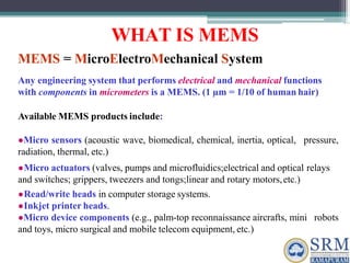
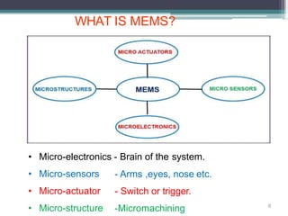
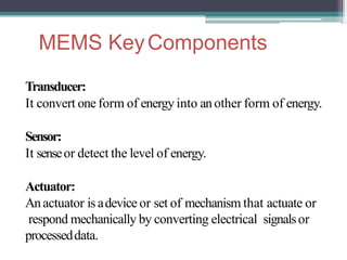
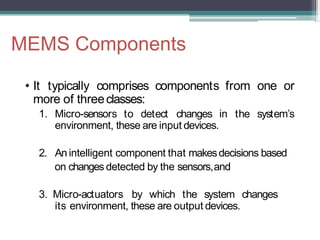
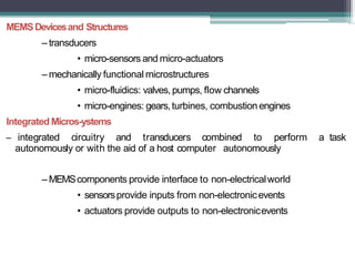
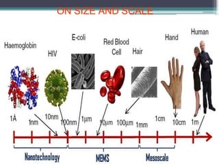
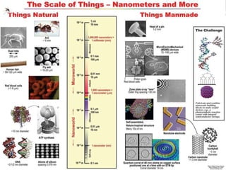
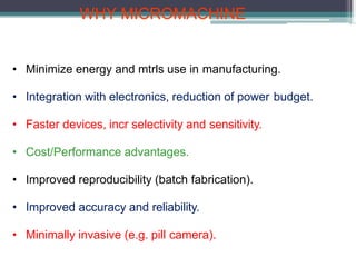
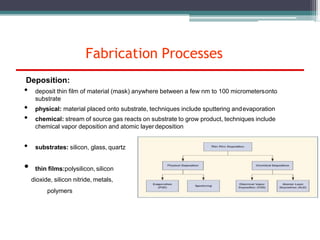
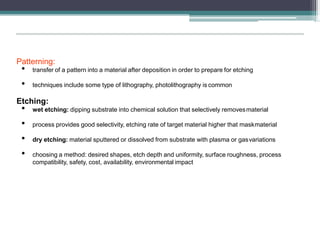
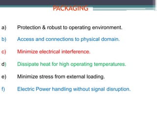
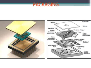
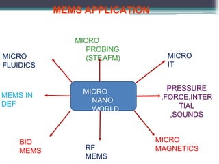
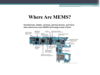
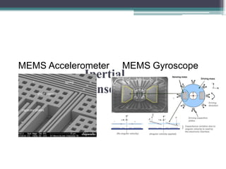
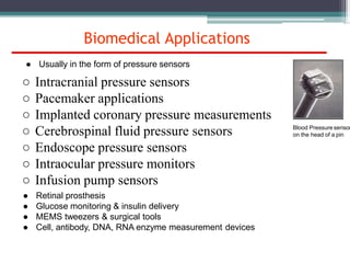
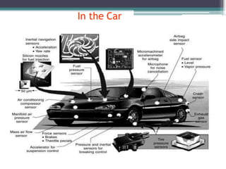
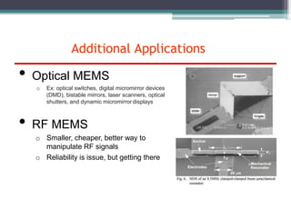
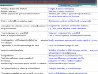
SUB CODE: PPE2109
FUNDAMENTALS OF MEMS
INTRODUCTION TO MEMS
(Unit 1)
WHAT IS MEMS?
• Technique of combining Electrical & Mechanical disiciplines.
• System of miniature dimensions.
• Micro fabrication technologies.
• Both sense on Micro scale effect on Macro scale
• Control the environment.
• Potential to effect all of our lives
5
• T
echnology of Microscopic devices & miniaturized
Integrated systems
• Components 1 and 100 micrometres in size.
• Devices 20 micrometres to a millimetre (i.e. 0.02 to
1.0 mm)
• Micro-sized components assembled & working together
as a system
INTRODUCTION
Inertia Sensor for Automobile “Air Bag”
Deployment System
Micro inertia sensor (accelerometer)in
place:
(Courtesy of Analog Devices, Inc)
Sensor-on-a-chip:
(the size of a
rice grain)
WHAT IS MEMS
MEMS = MicroElectroMechanical System
Any engineering system that performs electrical and mechanical functions
with components in micrometers is a MEMS. (1 µm = 1/10 of human hair)
Available MEMS products include:
●Micro sensors (acoustic wave, biomedical, chemical, inertia, optical, pressure,
radiation, thermal, etc.)
●Micro actuators (valves, pumps and microfluidics;electrical and optical relays
and switches; grippers, tweezers and tongs;linear and rotary motors,etc.)
●Read/write heads in computer storage systems.
●Inkjet printer heads.
●Micro device components (e.g., palm-top reconnaissance aircrafts, mini robots
and toys, micro surgical and mobile telecom equipment, etc.)
WHAT IS MEMS?
6
• Micro-electronics - Brain of the system.
• Micro-sensors
• Micro-actuator
• Micro-structure
- Arms ,eyes, nose etc.
- Switch or trigger.
-Micromachining
MEMS KeyComponents
Transducer:
It convert one form of energy into another form of energy.
Sensor:
It senseor detect the level of energy.
Actuator:
Anactuator is adevice or set of mechanism that actuate or
respond mechanically by converting electrical signalsor
processeddata.
MEMS Components
• It typically comprises components from one or
more of threeclasses:
1. Micro-sensors to detect changes in the system’s
environment, these are input devices.
2. An intelligent component that makesdecisions based
on changes detected by the sensors,and
3. Micro-actuators by which the system changes
its environment, these are output devices.
MEMSDevicesand Structures
– transducers
• micro-sensors and micro-actuators
– mechanically functional microstructures
• micro-fluidics: valves, pumps, flow channels
• micro-engines: gears,turbines, combustion engines
Integrated Micros-ystems
– integrated circuitry and transducers combined to perform a task
autonomously or with the aid of a host computer autonomously
– MEMScomponents provide interface to non-electricalworld
• sensorsprovide inputs from non-electronicevents
• actuators provide outputs to non-electronicevents
ON SIZE AND SCALE
WHY MICROMACHINE
• Minimize energy and mtrls use in manufacturing.
• Integration with electronics, reduction of power budget.
• Faster devices, incr selectivity and sensitivity.
• Cost/Performance advantages.
• Improved reproducibility (batch fabrication).
• Improved accuracy and reliability.
• Minimally invasive (e.g. pill camera).
The ENIAC Computer in
1946
A “Lap-top” Computerin
1996
Size: 106 down
Power: 106 up
Size: 108 down
Power: 108 up
A “Palm-top” Computer in2001
This spectacular miniaturization took place in 50 years!!
Miniaturization of Digital Computers
- A remarkable case ofminiaturization!
MINIATURIAZATION – The Principal Driving Force for
the 21st Century Industrial Technology
There has been increasing strong market demand for:
“Intelligent,”
“Robust,”
“Multi-functional,” and
“Low-cost”
industrial products.
Miniaturization is the only viable solution to satisfy such
market demand
Market Demand for Intelligent, Robusting,
Smaller, Multi-Functional Products - the
Mobil phones 10 YearsAgo:
Current State-of-the Art:
Transceive voice only
Transceive voice+ multi-media +
others (Video-camera, e-mails, calendar,
and access to Internet, GPS and a PC with
key pad input)
Size reduction
Palm-top WirelessPC
The only solution is to pack many miniature function components into the device
Rice grains
Micro Cars
(Courtesy of Denso Research Laboratories, Denso
Corporation, Aichi, Japan)
APPLICATION
MEMS in Daily Life
MEMS in Daily Life
Fabrication Processes
Deposition:
• deposit thin film of material (mask) anywhere between a few nm to 100 micrometersonto
substrate
• physical: material placed onto substrate, techniques include sputtering andevaporation
• chemical: stream of source gas reacts on substrate to grow product, techniques include
chemical vapor deposition and atomic layer deposition
• substrates: silicon, glass, quartz
• thin films:polysilicon, silicon
dioxide, silicon nitride, metals,
polymers
Patterning:
• transfer of a pattern into a material after deposition in order to prepare for etching
• techniques include some type of lithography, photolithography is common
Etching:
• wet etching: dipping substrate into chemical solution that selectively removesmaterial
• process provides good selectivity, etching rate of target material higher that maskmaterial
• dry etching: material sputtered or dissolved from substrate with plasma or gasvariations
• choosing a method: desired shapes, etch depth and uniformity, surface roughness, process
compatibility, safety, cost, availability, environmental impact
Fabrication Methods
Bulk Micromachining:
• oldest micromachining technology
• technique involves selective removal of substrate to produce mechanical
components
• accomplished by physical or chemical process with chemical being used
more for MEMS production
• chemical wet etching is popular because of high etch rate and selectivity
• isotropic wet etching: etch rate not dependent on crystallographic
orientation of substrate and etching moves at equal rates in all directions
• anisotropic wet etching: etch rate is dependent on crystallographic
orientation of substrate
Surface Micromachining:
• process starts with deposition of thin-film that acts as a temporary
mechanical layer (sacrificial layer)
• device layers are constructed on top
• deposition and patterning of structural layer
• removal of temporary layer to allow movement of structural layer
• benefits: variety of structure, sacrificial and etchant combinations, uses
single-sided wafer processing
• allows higher integration density and lower resultant per die cost
compared to bulk micromachining
• disadvantages: mechanical properties of most thin-films are usually
unknown and reproducibility of their mechanical properties
Wafer Bonding:
• Method that involves joining two or more
wafers together to create a wafer stack
• Three types of wafer bonding: direct bonding,
anodic bonding, and intermediate layerbonding
• All require substrates that are flat, smooth,
and clean in order to be efficient andsuccessful
High Aspect Ratio Fabrication (Silicon):
• Deep reactive ion etching (DRIE)
• Enables very high aspect ratio etches tobe
performed into silicon substrates
• Sidewalls of the etched holes are nearly vertical
• Depth of the etch can be hundreds
or even thousands of microns into the siliconsubstrate.
PACKAGING
a) Protection & robust to operating environment.
b) Access and connections to physical domain.
c) Minimize electrical interference.
d) Dissipate heat for high operating temperatures.
e) Minimize stress from external loading.
f) Electric Power handling without signal disruption.
PACKAGING
MEMS APPLICATION
MICRO
NANO
WORLD
MEMS IN
DEF
BIO
MEMS
MICRO
PROBING
(STF,AFM)
PRESSURE
,FORCE,INTER
TIAL
,SOUNDS
MICRO
MAGNETICS
RF
MEMS
MICRO
FLUIDICS
MICRO
IT
Where Are MEMS?
Smartphones, tablets, cameras, gaming devices, and many
other electronics have MEMS technology inside of them
MEMS Accelerometer MEMS Gyroscope
Inertial
Sensors
Biomedical Applications
Blood Pressure sensor
on the head of a pin
● Usually in the form of pressure sensors
○ Intracranial pressure sensors
○ Pacemaker applications
○ Implanted coronary pressure measurements
○ Cerebrospinal fluid pressure sensors
○ Endoscope pressure sensors
○ Intraocular pressure monitors
○ Infusion pump sensors
● Retinal prosthesis
● Glucose monitoring & insulin delivery
● MEMS tweezers & surgical tools
● Cell, antibody, DNA, RNA enzyme measurement devices
In the Car
• Optical MEMS
o Ex: optical switches, digital micromirror devices
(DMD), bistable mirrors, laser scanners, optical
shutters, and dynamic micromirror displays
• RF MEMS
o Smaller, cheaper, better way to
manipulate RF signals
o Reliability is issue, but getting there
Additional Applications
MEMS Advantages
• Suitable for high-volume and low-costproduction
• Reduced size
• Light weight
• Low power consumption
• High functionality
• Improved reliability
• Novel solutions and new applications
• Low cost
• Minimize Materials
DISADVANTAGES
capabilities and
manufacturing
• Impossible to transfer of Power
• Poly-Si (a brittle material), Cannot be load and force limitations.
• Disruptive technology, need different
competencies.
• Scaling, Packaging and Testing Issues.
• Challenges associated with developing
processes.
• Critical technological bottlenecks, economic feasibility.
• Time & expense.
FUTURE OF
MEMS
Challenges
• Access to Foundries.
• Design Simulation & Modelling
• Packaging and Testing
• Standardization
• Education and Training.
• Micro-sized objects allow us to go places where no objects
have gone before.
MEMS IN INDIA
• Jul 2002 first Lab ( IISc & CSI Ltd)
• Microelectronics Group & Suman Mashruwala Micro-
engineering Lab, IIT Bombay
• Fabrication facilities at:
• CEERI Pilani, ITI, BEL in Bangalore, SCL Chandigarh etc.
• Microelectronics Laboratories in close interaction with Indian
industries (BEL, DRDO , ISRO etc)
• MEMS work in Acoustic Sensor & Ultrasound sensors, in
GSLV & PSLV.
• Development of analytic tools and software.
CONCLUSION
• Promising technology for the 21st Century.
• Disruptive technology differs significantly from existing
technology.
• Challenges associated with developing manufacturing
processes.
• Automotive industry varied signatures in all fields.
• MEMS has gradually made its way out of research
laboratories and into everyday products.
Summary/Conclusion
Micro-Electro-Mechanical Systems are 1-100 micrometer
devices that convert electrical energy to mechanical energy
and vice-versa. The three basic steps to MEMS fabrication
are deposition, patterning, and etching. Due to their small
size, they can exhibit certain characteristics that their macro
equivalents can’t. MEMS produce benefits in speed,
complexity, power consumption, device area, and system
integration. These benefits make MEMS a great choice for
devices in numerous fields.
5 Key Concepts
1. MEMS are made up of microelectronics, microactuators,
microsensors, and microstructures.
2. The three basic steps to MEMS fabrication are: deposition,
patterning, and etching.
3. Chemical wet etching is popular because of high etch rate and
selectivity.
4. 3 types of MEMS transducers are: capacitive, thermal, and
piezoelectric.
5. The benefits of using MEMS: speed, power consumption, size,
system integration(all on one chip).
Comparison of Microelectronics and Microsystems
Microelectronics Microsystems (siliconbased)
Primarily 2-dimensional structures Complex 3-dimensional structure
Stationary structures May involve moving components
Transmit electricity for specific electrical functions Perform a great variety of specific biological,chemical,
electromechanical and optical functions
and plastic materials
IC die is protected from contacting media Delicate components are interfaced with workingmedia
Use single crystal silicon dies, silicon compounds, ceramics Use single crystal silicon dies and few other materials,
e.g. GaAs, quartz, polymers, ceramics and metals
Fewer components to be assembled Many more components to be assembled
Mature IC design methodologies Lack of engineering design methodology and standards
Complex patterns with high density of electrical
over substrates
circuitry Simpler patterns over substrates with simpler electrical circuitry
Large number of electrical feed-through and leads Fewer electrical feed-through and leads
Industrial standards available selections,
No industrial standard to follow in design, material
fabrication processes and packaging
Mass production Batch production, or on customer-need basis
Fabrication techniques are proven and well
documented
Many microfabrication techniques are used for
production, but with no standard procedures
Manufacturing techniques are proven and well documented Distinct manufacturingtechniques
Packaging technology is relatively well established Packaging technology is at the infant stage
Primarily involves electrical and chemical engineering Involves all disciplines of science and engineering

Mems unit 1 ppt

  • 1.
    SUB CODE: PPE2109 FUNDAMENTALSOF MEMS INTRODUCTION TO MEMS (Unit 1)
  • 2.
    WHAT IS MEMS? •Technique of combining Electrical & Mechanical disiciplines. • System of miniature dimensions. • Micro fabrication technologies. • Both sense on Micro scale effect on Macro scale • Control the environment. • Potential to effect all of our lives 5
  • 3.
    • T echnology ofMicroscopic devices & miniaturized Integrated systems • Components 1 and 100 micrometres in size. • Devices 20 micrometres to a millimetre (i.e. 0.02 to 1.0 mm) • Micro-sized components assembled & working together as a system INTRODUCTION
  • 4.
    Inertia Sensor forAutomobile “Air Bag” Deployment System Micro inertia sensor (accelerometer)in place: (Courtesy of Analog Devices, Inc) Sensor-on-a-chip: (the size of a rice grain)
  • 5.
    WHAT IS MEMS MEMS= MicroElectroMechanical System Any engineering system that performs electrical and mechanical functions with components in micrometers is a MEMS. (1 µm = 1/10 of human hair) Available MEMS products include: ●Micro sensors (acoustic wave, biomedical, chemical, inertia, optical, pressure, radiation, thermal, etc.) ●Micro actuators (valves, pumps and microfluidics;electrical and optical relays and switches; grippers, tweezers and tongs;linear and rotary motors,etc.) ●Read/write heads in computer storage systems. ●Inkjet printer heads. ●Micro device components (e.g., palm-top reconnaissance aircrafts, mini robots and toys, micro surgical and mobile telecom equipment, etc.)
  • 6.
    WHAT IS MEMS? 6 •Micro-electronics - Brain of the system. • Micro-sensors • Micro-actuator • Micro-structure - Arms ,eyes, nose etc. - Switch or trigger. -Micromachining
  • 7.
    MEMS KeyComponents Transducer: It convertone form of energy into another form of energy. Sensor: It senseor detect the level of energy. Actuator: Anactuator is adevice or set of mechanism that actuate or respond mechanically by converting electrical signalsor processeddata.
  • 8.
    MEMS Components • Ittypically comprises components from one or more of threeclasses: 1. Micro-sensors to detect changes in the system’s environment, these are input devices. 2. An intelligent component that makesdecisions based on changes detected by the sensors,and 3. Micro-actuators by which the system changes its environment, these are output devices.
  • 9.
    MEMSDevicesand Structures – transducers •micro-sensors and micro-actuators – mechanically functional microstructures • micro-fluidics: valves, pumps, flow channels • micro-engines: gears,turbines, combustion engines Integrated Micros-ystems – integrated circuitry and transducers combined to perform a task autonomously or with the aid of a host computer autonomously – MEMScomponents provide interface to non-electricalworld • sensorsprovide inputs from non-electronicevents • actuators provide outputs to non-electronicevents
  • 10.
  • 12.
    WHY MICROMACHINE • Minimizeenergy and mtrls use in manufacturing. • Integration with electronics, reduction of power budget. • Faster devices, incr selectivity and sensitivity. • Cost/Performance advantages. • Improved reproducibility (batch fabrication). • Improved accuracy and reliability. • Minimally invasive (e.g. pill camera).
  • 13.
    The ENIAC Computerin 1946 A “Lap-top” Computerin 1996 Size: 106 down Power: 106 up Size: 108 down Power: 108 up A “Palm-top” Computer in2001 This spectacular miniaturization took place in 50 years!! Miniaturization of Digital Computers - A remarkable case ofminiaturization!
  • 14.
    MINIATURIAZATION – ThePrincipal Driving Force for the 21st Century Industrial Technology There has been increasing strong market demand for: “Intelligent,” “Robust,” “Multi-functional,” and “Low-cost” industrial products. Miniaturization is the only viable solution to satisfy such market demand
  • 15.
    Market Demand forIntelligent, Robusting, Smaller, Multi-Functional Products - the Mobil phones 10 YearsAgo: Current State-of-the Art: Transceive voice only Transceive voice+ multi-media + others (Video-camera, e-mails, calendar, and access to Internet, GPS and a PC with key pad input) Size reduction Palm-top WirelessPC The only solution is to pack many miniature function components into the device
  • 16.
    Rice grains Micro Cars (Courtesyof Denso Research Laboratories, Denso Corporation, Aichi, Japan)
  • 17.
  • 18.
  • 19.
  • 20.
    Fabrication Processes Deposition: • depositthin film of material (mask) anywhere between a few nm to 100 micrometersonto substrate • physical: material placed onto substrate, techniques include sputtering andevaporation • chemical: stream of source gas reacts on substrate to grow product, techniques include chemical vapor deposition and atomic layer deposition • substrates: silicon, glass, quartz • thin films:polysilicon, silicon dioxide, silicon nitride, metals, polymers
  • 21.
    Patterning: • transfer ofa pattern into a material after deposition in order to prepare for etching • techniques include some type of lithography, photolithography is common Etching: • wet etching: dipping substrate into chemical solution that selectively removesmaterial • process provides good selectivity, etching rate of target material higher that maskmaterial • dry etching: material sputtered or dissolved from substrate with plasma or gasvariations • choosing a method: desired shapes, etch depth and uniformity, surface roughness, process compatibility, safety, cost, availability, environmental impact
  • 22.
    Fabrication Methods Bulk Micromachining: •oldest micromachining technology • technique involves selective removal of substrate to produce mechanical components • accomplished by physical or chemical process with chemical being used more for MEMS production • chemical wet etching is popular because of high etch rate and selectivity • isotropic wet etching: etch rate not dependent on crystallographic orientation of substrate and etching moves at equal rates in all directions • anisotropic wet etching: etch rate is dependent on crystallographic orientation of substrate
  • 23.
    Surface Micromachining: • processstarts with deposition of thin-film that acts as a temporary mechanical layer (sacrificial layer) • device layers are constructed on top • deposition and patterning of structural layer • removal of temporary layer to allow movement of structural layer • benefits: variety of structure, sacrificial and etchant combinations, uses single-sided wafer processing • allows higher integration density and lower resultant per die cost compared to bulk micromachining • disadvantages: mechanical properties of most thin-films are usually unknown and reproducibility of their mechanical properties
  • 25.
    Wafer Bonding: • Methodthat involves joining two or more wafers together to create a wafer stack • Three types of wafer bonding: direct bonding, anodic bonding, and intermediate layerbonding • All require substrates that are flat, smooth, and clean in order to be efficient andsuccessful High Aspect Ratio Fabrication (Silicon): • Deep reactive ion etching (DRIE) • Enables very high aspect ratio etches tobe performed into silicon substrates • Sidewalls of the etched holes are nearly vertical • Depth of the etch can be hundreds or even thousands of microns into the siliconsubstrate.
  • 26.
    PACKAGING a) Protection &robust to operating environment. b) Access and connections to physical domain. c) Minimize electrical interference. d) Dissipate heat for high operating temperatures. e) Minimize stress from external loading. f) Electric Power handling without signal disruption.
  • 27.
  • 28.
  • 29.
    Where Are MEMS? Smartphones,tablets, cameras, gaming devices, and many other electronics have MEMS technology inside of them
  • 30.
    MEMS Accelerometer MEMSGyroscope Inertial Sensors
  • 31.
    Biomedical Applications Blood Pressuresensor on the head of a pin ● Usually in the form of pressure sensors ○ Intracranial pressure sensors ○ Pacemaker applications ○ Implanted coronary pressure measurements ○ Cerebrospinal fluid pressure sensors ○ Endoscope pressure sensors ○ Intraocular pressure monitors ○ Infusion pump sensors ● Retinal prosthesis ● Glucose monitoring & insulin delivery ● MEMS tweezers & surgical tools ● Cell, antibody, DNA, RNA enzyme measurement devices
  • 32.
  • 33.
    • Optical MEMS oEx: optical switches, digital micromirror devices (DMD), bistable mirrors, laser scanners, optical shutters, and dynamic micromirror displays • RF MEMS o Smaller, cheaper, better way to manipulate RF signals o Reliability is issue, but getting there Additional Applications
  • 34.
    MEMS Advantages • Suitablefor high-volume and low-costproduction • Reduced size • Light weight • Low power consumption • High functionality • Improved reliability • Novel solutions and new applications • Low cost • Minimize Materials
  • 35.
    DISADVANTAGES capabilities and manufacturing • Impossibleto transfer of Power • Poly-Si (a brittle material), Cannot be load and force limitations. • Disruptive technology, need different competencies. • Scaling, Packaging and Testing Issues. • Challenges associated with developing processes. • Critical technological bottlenecks, economic feasibility. • Time & expense.
  • 36.
    FUTURE OF MEMS Challenges • Accessto Foundries. • Design Simulation & Modelling • Packaging and Testing • Standardization • Education and Training. • Micro-sized objects allow us to go places where no objects have gone before.
  • 37.
    MEMS IN INDIA •Jul 2002 first Lab ( IISc & CSI Ltd) • Microelectronics Group & Suman Mashruwala Micro- engineering Lab, IIT Bombay • Fabrication facilities at: • CEERI Pilani, ITI, BEL in Bangalore, SCL Chandigarh etc. • Microelectronics Laboratories in close interaction with Indian industries (BEL, DRDO , ISRO etc) • MEMS work in Acoustic Sensor & Ultrasound sensors, in GSLV & PSLV. • Development of analytic tools and software.
  • 38.
    CONCLUSION • Promising technologyfor the 21st Century. • Disruptive technology differs significantly from existing technology. • Challenges associated with developing manufacturing processes. • Automotive industry varied signatures in all fields. • MEMS has gradually made its way out of research laboratories and into everyday products.
  • 39.
    Summary/Conclusion Micro-Electro-Mechanical Systems are1-100 micrometer devices that convert electrical energy to mechanical energy and vice-versa. The three basic steps to MEMS fabrication are deposition, patterning, and etching. Due to their small size, they can exhibit certain characteristics that their macro equivalents can’t. MEMS produce benefits in speed, complexity, power consumption, device area, and system integration. These benefits make MEMS a great choice for devices in numerous fields.
  • 40.
    5 Key Concepts 1.MEMS are made up of microelectronics, microactuators, microsensors, and microstructures. 2. The three basic steps to MEMS fabrication are: deposition, patterning, and etching. 3. Chemical wet etching is popular because of high etch rate and selectivity. 4. 3 types of MEMS transducers are: capacitive, thermal, and piezoelectric. 5. The benefits of using MEMS: speed, power consumption, size, system integration(all on one chip).
  • 41.
    Comparison of Microelectronicsand Microsystems Microelectronics Microsystems (siliconbased) Primarily 2-dimensional structures Complex 3-dimensional structure Stationary structures May involve moving components Transmit electricity for specific electrical functions Perform a great variety of specific biological,chemical, electromechanical and optical functions and plastic materials IC die is protected from contacting media Delicate components are interfaced with workingmedia Use single crystal silicon dies, silicon compounds, ceramics Use single crystal silicon dies and few other materials, e.g. GaAs, quartz, polymers, ceramics and metals Fewer components to be assembled Many more components to be assembled Mature IC design methodologies Lack of engineering design methodology and standards Complex patterns with high density of electrical over substrates circuitry Simpler patterns over substrates with simpler electrical circuitry Large number of electrical feed-through and leads Fewer electrical feed-through and leads Industrial standards available selections, No industrial standard to follow in design, material fabrication processes and packaging Mass production Batch production, or on customer-need basis Fabrication techniques are proven and well documented Many microfabrication techniques are used for production, but with no standard procedures Manufacturing techniques are proven and well documented Distinct manufacturingtechniques Packaging technology is relatively well established Packaging technology is at the infant stage Primarily involves electrical and chemical engineering Involves all disciplines of science and engineering