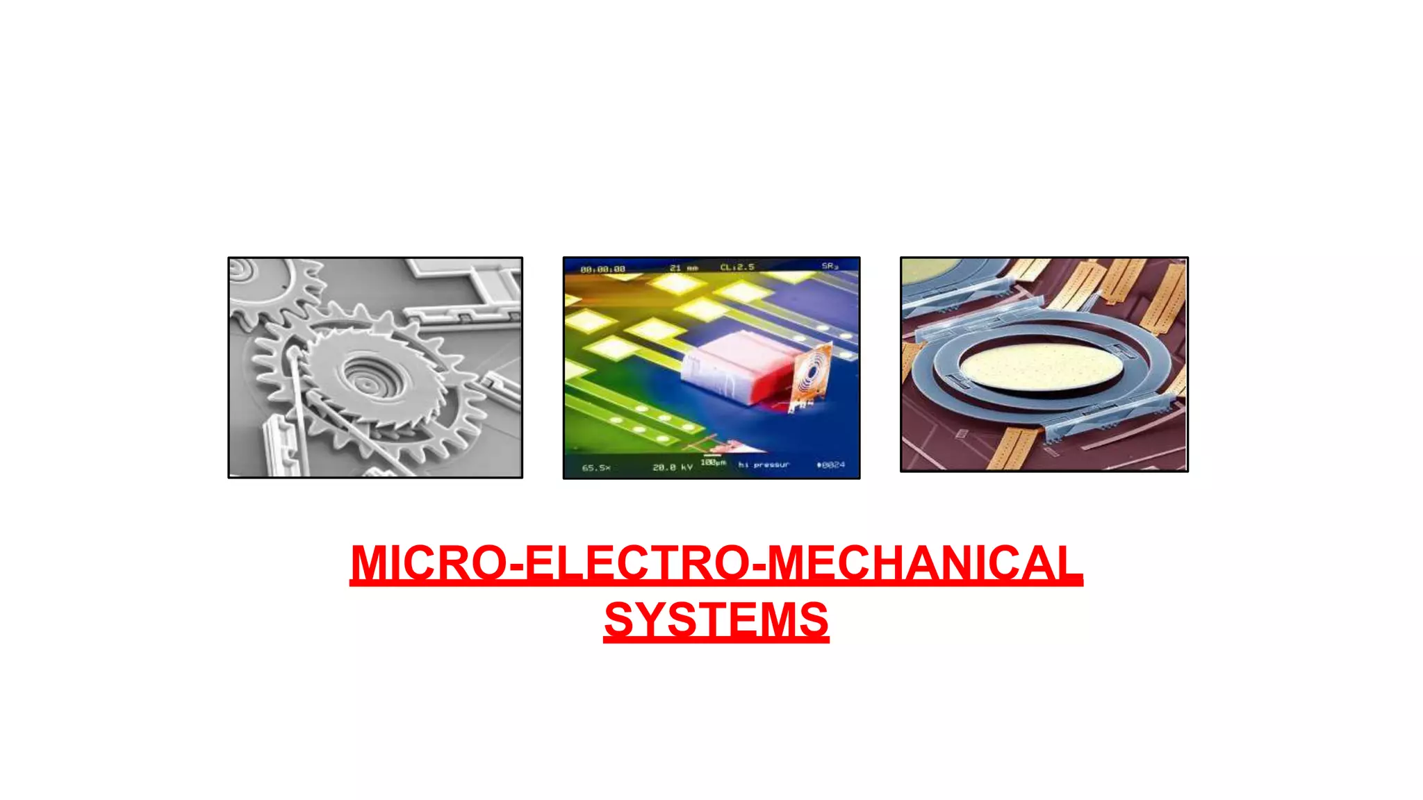
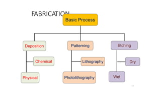
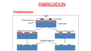
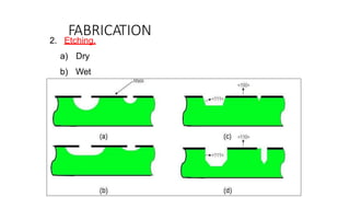
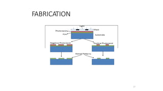
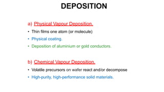
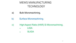
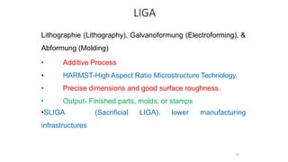
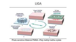
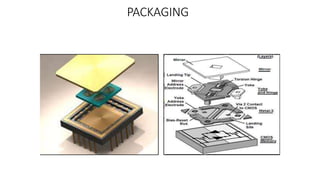
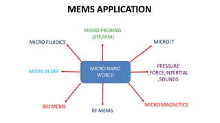
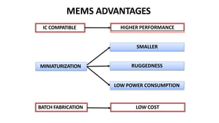
MICRO-ELECTRO-MECHANICAL
SYSTEMS
PREVIEW
• MEMS Introduction
• Fabrication and Basic techniques
• Applications
• Advantages & Disadvantages
• Future Trends
• MEMS in India
• Conclusion
• References
• T
echnology of Microscopic devices & miniaturized
Integrated systems
• Components 1 and 100 micrometres in size.
• Devices 20 micrometres to a millimetre (i.e. 0.02 to
1.0 mm)
• Micro-sized components assembled & working together
as a system
INTRODUCTION
Photo: http://
What are MEMS?
Micro-Electro-Mechanical Systems (MEMS)
• Miniaturized mechanical and electro-mechanical
elements (devices and structures)
• Sizes range from millimeters to fractions of
micrometers
• Some parts of the device have some sort of
mechanical functionality
• A.K.A. Microsystems Technology or
Micromachined Devices
• Technique of combining Electrical & Mechanical disiciplines.
• System of miniature dimensions.
• Micro fabrication technologies.
• Both sense on Micro scale effect on Macro scale
• Control the environment.
• Potential to effect all of our lives
5
Process flow
• Design
– Numerical
• Coventorware, Intellisuite, COMSOL, ANSYS etc,.
– Analytical
• Fabrication
• Assembling
• Packaging
• Testing
– At die level
– At packaging level
6
WHAT IS MEMS?
6
• Micro-electronics - Brain of the system.
• Micro-sensors
• Micro-actuator
• Micro-structure
- Arms ,eyes, nose etc.
- Switch or trigger.
-Micromachining
WHY MICROMACHINE
• Minimize energy and mtrls use in manufacturing.
• Integration with electronics, reduction of power budget.
• Faster devices, incr selectivity and sensitivity.
• Cost/Performance advantages.
• Improved reproducibility (batch fabrication).
• Improved accuracy and reliability.
• Minimally invasive (e.g. pill camera).
SUBTRATES
• Silicon
• Glass
• Polymers
• Metals - Metals like Gold, Ni, Al, Cr, Pl, and Ag
• Ceramics 12
10
Why Silicon?
• Not only a semiconductor
• Very good structural material comparable with that of steel
– Young’s modulus
– Poisson’s ratio
– Yield strength
• Derives fabrication principles from well established Si based
IC technology
• Electronic circuits
– Solid and compact
• MEMS structures
– holes, cavity, channels, cantilevers, membranes, etc,
FABRICATION
13
Basic Process
Deposition Patterning Etching
Chemical
Wet
Dry
Physical
Lithography
Photolithography
BASIC PROCESS OF FABRICATION
• Deposition
– Deposition that happen because of a Chemical reaction or
Physical reaction.
• Patterning
– Transfer to a photosensitive material, exposure to UV light.
– Developed in solution after exposure to UV.
– Material Etch away.
• Etching
– Strong acid to cut into the unprotected parts of a metal
surface to create a design.
– Two classes :
• Wet Etching
• Dry Etching.
14
FABRICATION
15
Photolithography.
FABRICATION
16
2. Etching.
a) Dry
b) Wet
FABRICATION
17
a) Photolithography.
DEPOSITION
a) Physical Vapour Deposition.
• Thin films one atom (or molecule)
• Physical coating.
• Deposition of aluminium or gold conductors.
b) Chemical Vapour Deposition.
• Volatile precursors on wafer react and/or decompose
• High-purity, high-performance solid materials.
MEMS MANUFACTURING
TECHNOLOGY
19
a) Bulk Micromachining.
b) Surface Micromachining.
c) High Aspect Ratio (HAR) Si Micromachining.
•
•
LIGA
SLIGA
LIGA
20
Lithographie (Lithography), Galvanoformung (Electroforming), &
Abformung (Molding)
• Additive Process
• HARMST-High Aspect Ratio Microstructure Technology.
• Precise dimensions and good surface roughness.
• Output- Finished parts, molds, or stamps
•SLIGA (Sacrificial LIGA). lower manufacturing
infrastructures
LIGA
Photo sensitive Material PMMA –Poly methyl metha crylate
PACKAGING
a) Protection & robust to operating environment.
b) Access and connections to physical domain.
c) Minimize electrical interference.
d) Dissipate heat for high operating temperatures.
e) Minimize stress from external loading.
f) Electric Power handling without signal disruption.
PACKAGING
MEMS APPLICATION
MICRO NANO
WORLD
MEMS IN DEF
BIO MEMS
MICRO PROBING
(STF,AFM)
PRESSURE
,FORCE,INTERTIAL
,SOUNDS
MICRO MAGNETICS
RF MEMS
MICRO FLUIDICS MICRO IT
MEMS ADVANTAGES
IC COMPATIBLE
LOW COST
RUGGEDNESS
SMALLER
BATCH FABRICATION
MINIATURIZATION
LOW POWER CONSUMPTION
HIGHER PERFORMANCE
DISADVANTAGES
capabilities and
manufacturing
• Impossible to transfer of Power impossible.
• Poly-Si (a brittle material), Cannot be load and force limitations.
• Disruptive technology, need different
competencies.
• Scaling, Packaging and Testing Issues.
• Challenges associated with developing
processes.
• Critical technological bottlenecks, economic feasibility.
• Time & expense.
MEMS Sensors
• Turn physical phenomena into measurable
electrical signals
• Most (if not all) incorporate
circuitry/components to interpret electrical
signals
• Some have no moving parts
MEMS Sensors - Accelerometer
Analog Output
Accelerometer Module
$2.70
MEMS Devices
• Some are just scaled down versions of other
systems
• Use electric or electromagnetic principles to
control mechanical effects
• Commonly used in groups rather than
individually
Some MEMS Applications
Microchain Drive
(Microchain &
Gears)
FUTURE OF MEMS
Challenges
• Access to Foundries.
• Design Simulation & Modelling
• Packaging and Testing
• Standardization
• Education and Training.
• Micro-sized objects allow us to go places where no objects
have gone before.

Mems unit 1-lec_1

  • 1.
  • 2.
    PREVIEW • MEMS Introduction •Fabrication and Basic techniques • Applications • Advantages & Disadvantages • Future Trends • MEMS in India • Conclusion • References
  • 3.
    • T echnology ofMicroscopic devices & miniaturized Integrated systems • Components 1 and 100 micrometres in size. • Devices 20 micrometres to a millimetre (i.e. 0.02 to 1.0 mm) • Micro-sized components assembled & working together as a system INTRODUCTION
  • 4.
    Photo: http:// What areMEMS? Micro-Electro-Mechanical Systems (MEMS) • Miniaturized mechanical and electro-mechanical elements (devices and structures) • Sizes range from millimeters to fractions of micrometers • Some parts of the device have some sort of mechanical functionality • A.K.A. Microsystems Technology or Micromachined Devices
  • 5.
    • Technique ofcombining Electrical & Mechanical disiciplines. • System of miniature dimensions. • Micro fabrication technologies. • Both sense on Micro scale effect on Macro scale • Control the environment. • Potential to effect all of our lives 5
  • 6.
    Process flow • Design –Numerical • Coventorware, Intellisuite, COMSOL, ANSYS etc,. – Analytical • Fabrication • Assembling • Packaging • Testing – At die level – At packaging level 6
  • 7.
    WHAT IS MEMS? 6 •Micro-electronics - Brain of the system. • Micro-sensors • Micro-actuator • Micro-structure - Arms ,eyes, nose etc. - Switch or trigger. -Micromachining
  • 8.
    WHY MICROMACHINE • Minimizeenergy and mtrls use in manufacturing. • Integration with electronics, reduction of power budget. • Faster devices, incr selectivity and sensitivity. • Cost/Performance advantages. • Improved reproducibility (batch fabrication). • Improved accuracy and reliability. • Minimally invasive (e.g. pill camera).
  • 9.
    SUBTRATES • Silicon • Glass •Polymers • Metals - Metals like Gold, Ni, Al, Cr, Pl, and Ag • Ceramics 12
  • 10.
    10 Why Silicon? • Notonly a semiconductor • Very good structural material comparable with that of steel – Young’s modulus – Poisson’s ratio – Yield strength • Derives fabrication principles from well established Si based IC technology • Electronic circuits – Solid and compact • MEMS structures – holes, cavity, channels, cantilevers, membranes, etc,
  • 11.
    FABRICATION 13 Basic Process Deposition PatterningEtching Chemical Wet Dry Physical Lithography Photolithography
  • 12.
    BASIC PROCESS OFFABRICATION • Deposition – Deposition that happen because of a Chemical reaction or Physical reaction. • Patterning – Transfer to a photosensitive material, exposure to UV light. – Developed in solution after exposure to UV. – Material Etch away. • Etching – Strong acid to cut into the unprotected parts of a metal surface to create a design. – Two classes : • Wet Etching • Dry Etching. 14
  • 13.
  • 14.
  • 15.
  • 16.
    DEPOSITION a) Physical VapourDeposition. • Thin films one atom (or molecule) • Physical coating. • Deposition of aluminium or gold conductors. b) Chemical Vapour Deposition. • Volatile precursors on wafer react and/or decompose • High-purity, high-performance solid materials.
  • 17.
    MEMS MANUFACTURING TECHNOLOGY 19 a) BulkMicromachining. b) Surface Micromachining. c) High Aspect Ratio (HAR) Si Micromachining. • • LIGA SLIGA
  • 18.
    LIGA 20 Lithographie (Lithography), Galvanoformung(Electroforming), & Abformung (Molding) • Additive Process • HARMST-High Aspect Ratio Microstructure Technology. • Precise dimensions and good surface roughness. • Output- Finished parts, molds, or stamps •SLIGA (Sacrificial LIGA). lower manufacturing infrastructures
  • 19.
    LIGA Photo sensitive MaterialPMMA –Poly methyl metha crylate
  • 20.
    PACKAGING a) Protection &robust to operating environment. b) Access and connections to physical domain. c) Minimize electrical interference. d) Dissipate heat for high operating temperatures. e) Minimize stress from external loading. f) Electric Power handling without signal disruption.
  • 21.
  • 22.
    MEMS APPLICATION MICRO NANO WORLD MEMSIN DEF BIO MEMS MICRO PROBING (STF,AFM) PRESSURE ,FORCE,INTERTIAL ,SOUNDS MICRO MAGNETICS RF MEMS MICRO FLUIDICS MICRO IT
  • 23.
    MEMS ADVANTAGES IC COMPATIBLE LOWCOST RUGGEDNESS SMALLER BATCH FABRICATION MINIATURIZATION LOW POWER CONSUMPTION HIGHER PERFORMANCE
  • 24.
    DISADVANTAGES capabilities and manufacturing • Impossibleto transfer of Power impossible. • Poly-Si (a brittle material), Cannot be load and force limitations. • Disruptive technology, need different competencies. • Scaling, Packaging and Testing Issues. • Challenges associated with developing processes. • Critical technological bottlenecks, economic feasibility. • Time & expense.
  • 25.
    MEMS Sensors • Turnphysical phenomena into measurable electrical signals • Most (if not all) incorporate circuitry/components to interpret electrical signals • Some have no moving parts
  • 26.
    MEMS Sensors -Accelerometer
  • 27.
    MEMS Sensors -Accelerometer
  • 28.
    MEMS Sensors -Accelerometer
  • 29.
    MEMS Sensors -Accelerometer Analog Output Accelerometer Module $2.70
  • 30.
    MEMS Devices • Someare just scaled down versions of other systems • Use electric or electromagnetic principles to control mechanical effects • Commonly used in groups rather than individually
  • 31.
    Some MEMS Applications MicrochainDrive (Microchain & Gears)
  • 32.
    FUTURE OF MEMS Challenges •Access to Foundries. • Design Simulation & Modelling • Packaging and Testing • Standardization • Education and Training. • Micro-sized objects allow us to go places where no objects have gone before.