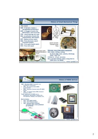
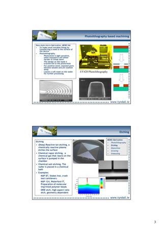
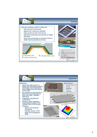
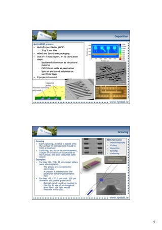
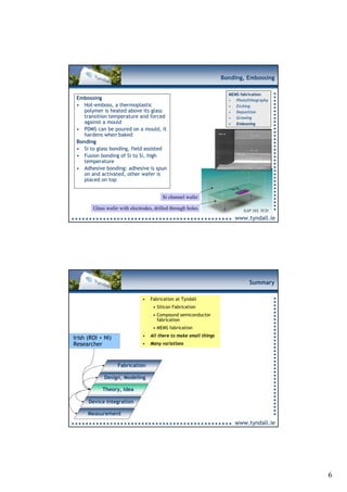
Tyndall National Institute


                                            MEMS Fabrication at
                                                  Tyndall

                                                 NAP Open Day Presentations
                                                  Wednesday 7th May 2008


                                                      – Jaap Verheggen


                                                                 www.tyndall.ie


                                                                      Introduction

Contents
• Introduction
    – A history of small
      mechanical things
    – How MEMS came about
• MEMS fabrication                • MEMS is a big word
                                     – Micro ‘Electro’ Mechanical systems
    – Photolithography
                                         • Or Microsystems Technology or
    – Etching                              Micromechatronics or
    – Deposition                           Micromachines
    – Growing                        – Small Movable Parts
    – Embossing, Bonding             – Applications in: bio, opto, RF,
                                       thermal, radio, electro, etc…
                                     – Either Sensor, process or actuator


        MEMS fabrication: the process of making small movable
         MEMS fabrication: the process of making small movable
        things by transferring a mask to the surface of the device
         things by transferring a mask to the surface of the device
                                                                 www.tyndall.ie


                                                                                     1
History of Small Mechanical Things

The watch
1480 - P.Henlein creates a
   springloaded pocketwatch
1659 - C.Huygens invents the
   Remontoire, more accurate
1709 - Jewel bearings are used
1844 - A.LeCoultre invents the
   millionometre, Micrometer.
1957 - Battery driven watch
1960 – First electronic watch
   (transistor pulser)                                Quartz resonator
1962 - First quarz-based watch                        Transistor pulser
1972 - First LCD watch                                            Ruby


                            Watchmakers lathe,     Old-style ‘micro’fabrication equipment
                            achieves accuracy of   Drill, lathe, milling, cutting
                            ‘10 μm’
                                                       by sharp edge, laser, plasma, discharge,
                                                       water, sand, etc.
                                                   Limited to ~25 μm accuracy
                                                   Not a parallel method, takes a long time to
                                                       make (this is not MEMS)
                                                                                   www.tyndall.ie


                                                                          History of MEMS devices

 1987 – The term MEMS ‘invented’ at a
     transducers conference
 • 1991 – AD commercialize MEMS
     accelerometer
 • 1993 – Raytheon Commercialize RF MEMS
     Switch
 • 1993 – TI commercialize DMD (research
     started in 1977)
 Today, application of MEMS are in
     automotive, gyroscopes, mobile com,
     microphones, displays, bio medical, etc.

 Back in history
 • 1977 – First inkjet nozzle
 • 1972 – First Pressure sensor
 • 1967 – Resonant gate transistor
      – Transistor with a micro-pendulum
          for oscillation


                                                                                   www.tyndall.ie


                                                                                                    2
Photolithography based machining


New-style micro-fabrication, MEMS fab
• To make small movable things by
   transferring a mask to the surface of
   the device
• Photolithography
     – Photoresist is light sensitive,
        when exposed it will either
        harden or break down
     – The design on the mask is
        transferred to the photoresist
     – For positive resist, exposed parts
        become soluble and are washed
        away
     – Leaves a soft mask on the wafer      30 µm
                                                EV420 Photolithography
        for further processing


                                                                         www.tyndall.ie


                                                                                Etching

                                                                     MEMS fabrication
Etching                                                              • Photolithography
• (Deep) Reactive ion etching, a                                     • Etching
  chemically reactive plasma                                         • Deposition
  etches the surface                                                 • Growing
• Chemical vapor etching, a                                          • Embossing
  chemical gas that reacts on the
  surface is pumped in the
  chamber
• Chemical wet etching, The
  wafer is placed in a chemical             30 µm
  bath
• Examples:
   – NAP 87, Stokes Inst, crash
     test cantilevers
   – NAP 124, Waterford IT,
     Preparation of molecular
     imprinted polymer beads
   – DRIE etch, high aspect ratio
     etch, geometry dependent

                                                                         www.tyndall.ie


                                                                                          3
Etching


 Crash test cantilevers, NAP 87, Stokes Inst.
    – KOH wet etch from the back
    – Deposit etch, Aluminum, polyimide
    – Deep reactive Ion Etch from the top
    – Wet etch of polyimide and aluminum to release
      the device
    – Shock test, acceleration as function of time to
      obtain material properties of silicon


    Si Wafer, 525 µm                100 µm


     = Silicon Oxide, 50nm         = Polyimide, Sacrificial 10µm
     = Alumium, Sacrificial, 6µm


                                                                     www.tyndall.ie


                                                                          Deposition

Deposition                                                         MEMS fabrication
• Sputtering, argon atoms in a                                     • Photolithography
   plasma are accelerated towards a                                • Etching
   solid target, this bombardment                                  • Deposition
   ejects target atoms that deposit                                • Growing
   on the wafer
                                                                   • Embossing
• Spin casting, an uncured resin is
   poured on a spinning wafer to
   form a thin layer, solidified
   afterwards
• Evaporation, deposition by
   condensation
• Chemical vapour deposition,
   volatile gasses pumped in the
   chamber react on the surface
• Examples:
    – NAP 35, CIT Ultrasonic
        membranes
    – Humidity sensors, CTVR
    – Wafer level Packaging of
        MEMS

                                                                     www.tyndall.ie


                                                                                        4
Deposition

 Multi-MEMS process
 • Multi-Project Wafer (MPW)
      – 3 by 3 mm dies
 • MEMS and Zero-Level packaging
 • Use of 17 mask layers, +120 fabrication
    steps
      – Sputtered Aluminium as structural
        material
      – CVD Silicon oxide as passivation
      – Spin on and cured polyimide as
        sacrificial layer
 • 8 projects involved

              Capacitor
              plates
Moisture-sensitive
polyimide


                                                         www.tyndall.ie


                                                                 Growing

                                                       MEMS fabrication
   Growing
                                                       • Photolithography
   • Electroplating, a metal is plated onto
      the surface in a photoresist mould to            • Etching
      form a structure                                 • Deposition
   • Oxidizing, in a oxide rich environment,           • Growing
      a layer of silicon oxide is created on           • Embossing
      the surface, this also consumes some
      silicon
   Examples:
   • For Nap 103, TCD, 25 µm copper pillars
      were electroplated.
        – The pillars are connected to       30   µm
           electrodes
        – A channel is created over the
           pillars for electrohydrodynamic
           flow
   • For Nap 112, CIT, 2 µm thick, 100 µm
      diameter discs were grown on Si.
        – Optical signal could be coupled in
           the disc by use of an elongated
           glass fiber, the light would
           resonate in the disc.


                                                         www.tyndall.ie


                                                                            5
Bonding, Embossing

                                                                      MEMS fabrication
 Embossing                                                            • Photolithography
 • Hot-emboss, a thermoplastic                                        • Etching
    polymer is heated above its glass                                 • Deposition
    transition temperature and forced                                 • Growing
    against a mould                                                   • Embossing
 • PDMS can be poured on a mould, it
    hardens when baked
 Bonding
 • Si to glass bonding, field assisted
 • Fusion bonding of Si to Si, high
    temperature
 • Adhesive bonding: adhesive is spun
    on and activated, other wafer is
    placed on top


                                         Si channel wafer

        Glass wafer with electrodes, drilled through holes                  NAP 103, TCD
                                                                        www.tyndall.ie


                                                                               Summary

                               •   Fabrication at Tyndall
                                    • Silicon Fabrication
                                    • Compound semiconductor
                                      fabrication
                                    • MEMS fabrication
                               •   All there to make small things
Irish (ROI + NI)
Researcher                     •   Many variations


                   Fabrication

             Design, Modeling

            Theory, Idea

      Device Integration

      Measurement
                                                                        www.tyndall.ie


                                                                                           6
know more & more & more…


                                   – Thanks for your attention


    For more information, visit www.Tyndall.ie,
www.Tyndall.ie/research/MEMS and www.Tyndall.ie/NAP
                                                www.tyndall.ie


                                                                 7

Jv Nap Openday 7 5 08

  • 1.
    Tyndall National Institute MEMS Fabrication at Tyndall NAP Open Day Presentations Wednesday 7th May 2008 – Jaap Verheggen www.tyndall.ie Introduction Contents • Introduction – A history of small mechanical things – How MEMS came about • MEMS fabrication • MEMS is a big word – Micro ‘Electro’ Mechanical systems – Photolithography • Or Microsystems Technology or – Etching Micromechatronics or – Deposition Micromachines – Growing – Small Movable Parts – Embossing, Bonding – Applications in: bio, opto, RF, thermal, radio, electro, etc… – Either Sensor, process or actuator MEMS fabrication: the process of making small movable MEMS fabrication: the process of making small movable things by transferring a mask to the surface of the device things by transferring a mask to the surface of the device www.tyndall.ie 1
  • 2.
    History of SmallMechanical Things The watch 1480 - P.Henlein creates a springloaded pocketwatch 1659 - C.Huygens invents the Remontoire, more accurate 1709 - Jewel bearings are used 1844 - A.LeCoultre invents the millionometre, Micrometer. 1957 - Battery driven watch 1960 – First electronic watch (transistor pulser) Quartz resonator 1962 - First quarz-based watch Transistor pulser 1972 - First LCD watch Ruby Watchmakers lathe, Old-style ‘micro’fabrication equipment achieves accuracy of Drill, lathe, milling, cutting ‘10 μm’ by sharp edge, laser, plasma, discharge, water, sand, etc. Limited to ~25 μm accuracy Not a parallel method, takes a long time to make (this is not MEMS) www.tyndall.ie History of MEMS devices 1987 – The term MEMS ‘invented’ at a transducers conference • 1991 – AD commercialize MEMS accelerometer • 1993 – Raytheon Commercialize RF MEMS Switch • 1993 – TI commercialize DMD (research started in 1977) Today, application of MEMS are in automotive, gyroscopes, mobile com, microphones, displays, bio medical, etc. Back in history • 1977 – First inkjet nozzle • 1972 – First Pressure sensor • 1967 – Resonant gate transistor – Transistor with a micro-pendulum for oscillation www.tyndall.ie 2
  • 3.
    Photolithography based machining New-stylemicro-fabrication, MEMS fab • To make small movable things by transferring a mask to the surface of the device • Photolithography – Photoresist is light sensitive, when exposed it will either harden or break down – The design on the mask is transferred to the photoresist – For positive resist, exposed parts become soluble and are washed away – Leaves a soft mask on the wafer 30 µm EV420 Photolithography for further processing www.tyndall.ie Etching MEMS fabrication Etching • Photolithography • (Deep) Reactive ion etching, a • Etching chemically reactive plasma • Deposition etches the surface • Growing • Chemical vapor etching, a • Embossing chemical gas that reacts on the surface is pumped in the chamber • Chemical wet etching, The wafer is placed in a chemical 30 µm bath • Examples: – NAP 87, Stokes Inst, crash test cantilevers – NAP 124, Waterford IT, Preparation of molecular imprinted polymer beads – DRIE etch, high aspect ratio etch, geometry dependent www.tyndall.ie 3
  • 4.
    Etching Crash testcantilevers, NAP 87, Stokes Inst. – KOH wet etch from the back – Deposit etch, Aluminum, polyimide – Deep reactive Ion Etch from the top – Wet etch of polyimide and aluminum to release the device – Shock test, acceleration as function of time to obtain material properties of silicon Si Wafer, 525 µm 100 µm = Silicon Oxide, 50nm = Polyimide, Sacrificial 10µm = Alumium, Sacrificial, 6µm www.tyndall.ie Deposition Deposition MEMS fabrication • Sputtering, argon atoms in a • Photolithography plasma are accelerated towards a • Etching solid target, this bombardment • Deposition ejects target atoms that deposit • Growing on the wafer • Embossing • Spin casting, an uncured resin is poured on a spinning wafer to form a thin layer, solidified afterwards • Evaporation, deposition by condensation • Chemical vapour deposition, volatile gasses pumped in the chamber react on the surface • Examples: – NAP 35, CIT Ultrasonic membranes – Humidity sensors, CTVR – Wafer level Packaging of MEMS www.tyndall.ie 4
  • 5.
    Deposition Multi-MEMS process • Multi-Project Wafer (MPW) – 3 by 3 mm dies • MEMS and Zero-Level packaging • Use of 17 mask layers, +120 fabrication steps – Sputtered Aluminium as structural material – CVD Silicon oxide as passivation – Spin on and cured polyimide as sacrificial layer • 8 projects involved Capacitor plates Moisture-sensitive polyimide www.tyndall.ie Growing MEMS fabrication Growing • Photolithography • Electroplating, a metal is plated onto the surface in a photoresist mould to • Etching form a structure • Deposition • Oxidizing, in a oxide rich environment, • Growing a layer of silicon oxide is created on • Embossing the surface, this also consumes some silicon Examples: • For Nap 103, TCD, 25 µm copper pillars were electroplated. – The pillars are connected to 30 µm electrodes – A channel is created over the pillars for electrohydrodynamic flow • For Nap 112, CIT, 2 µm thick, 100 µm diameter discs were grown on Si. – Optical signal could be coupled in the disc by use of an elongated glass fiber, the light would resonate in the disc. www.tyndall.ie 5
  • 6.
    Bonding, Embossing MEMS fabrication Embossing • Photolithography • Hot-emboss, a thermoplastic • Etching polymer is heated above its glass • Deposition transition temperature and forced • Growing against a mould • Embossing • PDMS can be poured on a mould, it hardens when baked Bonding • Si to glass bonding, field assisted • Fusion bonding of Si to Si, high temperature • Adhesive bonding: adhesive is spun on and activated, other wafer is placed on top Si channel wafer Glass wafer with electrodes, drilled through holes NAP 103, TCD www.tyndall.ie Summary • Fabrication at Tyndall • Silicon Fabrication • Compound semiconductor fabrication • MEMS fabrication • All there to make small things Irish (ROI + NI) Researcher • Many variations Fabrication Design, Modeling Theory, Idea Device Integration Measurement www.tyndall.ie 6
  • 7.
    know more &more & more… – Thanks for your attention For more information, visit www.Tyndall.ie, www.Tyndall.ie/research/MEMS and www.Tyndall.ie/NAP www.tyndall.ie 7