Downloaded 1,083 times

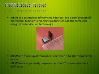

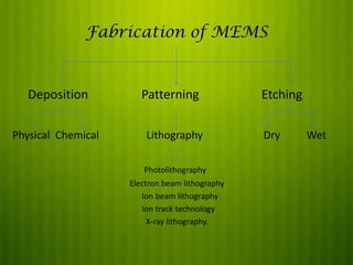
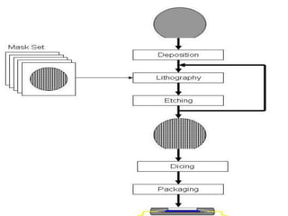

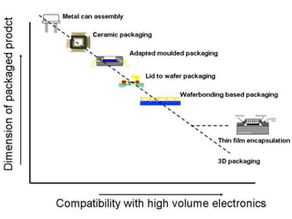


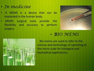
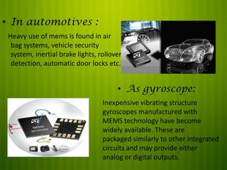
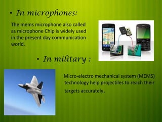


This document discusses Micro Electro Mechanical Systems (MEMS). MEMS are tiny devices that combine mechanical and electrical components using microfabrication technology. They range in size from 1 to 100 micrometers. The document outlines common MEMS fabrication techniques like deposition, patterning through lithography, and etching. It also discusses MEMS applications in areas like automotive, medical, sensors, and more. MEMS offer benefits like low energy use and improved accuracy but challenges include high costs and complex design procedures. The future of MEMS is seen as integrating more sensors, energy modules, and wireless capabilities to create entirely new product categories.