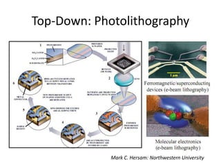
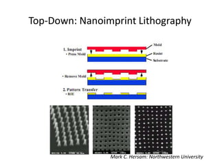
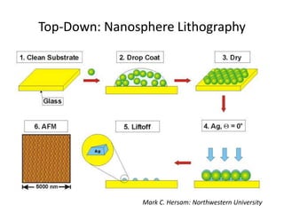
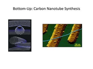
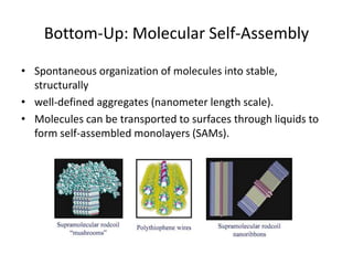
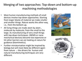
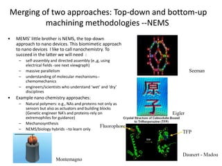
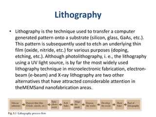
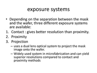
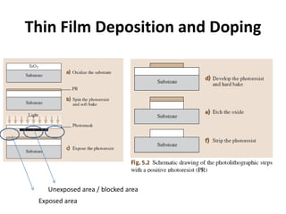
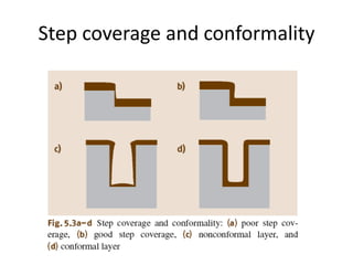
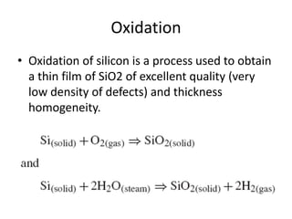
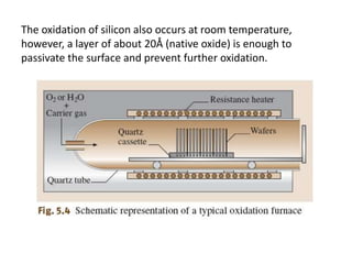
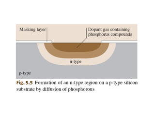
ETE444/544 :: Lecture 5
    Introduction to
   Micro Fabrication
        Chapter 5
  Springer Handbook of
Nanotechnology (Page 147-)
Introduction
• Recent innovations in the area of micro fabrication
  have created a unique opportunity for manufacturing
  structures in the nanometer–millimeter range. We
  can fabricate novel electronic, optical, magnetic,
  mechanical, and chemical/biological devices with
  applications ranging from sensors to computation
  and control.
Nano Fabrication
•   Basic Microfabrication Techniques
     – Lithography
     – Thin Film Deposition and Doping
     – Etching and Substrate Removal
     – Substrate Bonding
Fabrication
• Top-down: Chisel away material to make
  nanoscale objects
• Bottom-up: Assemble nanoscale objects out of
  even smaller units (e.g., atoms and molecules)
• Ultimate Goal: Dial in the properties that you
  want by designing and building at the scale of
  nature (i.e., the nanoscale)
Top-Down: Photolithography


             Mark C. Hersam: Northwestern University
Top-Down: Nanoimprint Lithography


                Mark C. Hersam: Northwestern University
Top-Down: Nanosphere Lithography


                Mark C. Hersam: Northwestern University
Bottom-Up: Carbon Nanotube Synthesis
Bottom-Up: Molecular Self-Assembly

• Spontaneous organization of molecules into stable,
  structurally
• well-defined aggregates (nanometer length scale).
• Molecules can be transported to surfaces through liquids to
  form self-assembled monolayers (SAMs).
Merging of two approaches: Top-down and bottom-up
               machining methodologies
• Most human manufacturing methods of small
  devices involve top-down approaches. Starting
  from larger blocks of material we make smaller
  and smaller things. Nature works the other way,
  i.e., from the bottom-up.
• All living things are made atom by atom ,
  molecule by molecule; from the small to the
  large. As manufacturing of very small things
  with top-down techniques (NEMS or nano
  mechanical devices) become too expensive or
  hit other barriers we are looking at nature for
  guidance (biomimetics).
• Further miniaturization might be inspired by
  biology but will most likely be different again
  from nature -- the drivers for human and
  natural manufacturing techniques are very
  different.
Merging of two approaches: Top-down and bottom-up
         machining methodologies --NEMS
•   MEMS’ little brother is NEMS, the top-down
    approach to nano devices. This biomimetic approach
    to nano devices I like to call nanochemistry. To
    succeed in the latter we will need :
     –   self-assembly and directed assembly (e.,g, using
         electrical fields -see next viewgraph)
     –   massive parallelism                                             Seeman
     –   understanding of molecular mechanisms--
         chemomechanics
     –   engineers/scientists who understand ‘wet’ and ‘dry’
         disciplines
•   Example nano chemistry approaches:
     –   Natural polymers: e.g., NAs and proteins not only as
         sensors but also as actuators and building blocks
         (Genetic engineer NA’s and proteins-rely on            Eigler
         extremophiles for guidance)
     –   Mechanosynthesis
     –   NEMS/biology hybrids --to learn only


                          Montemagno                            Daunert - Madou
Lithography
• Lithography is the technique used to transfer a computer
  generated pattern onto a substrate (silicon, glass, GaAs, etc.).
  This pattern is subsequently used to etch an underlying thin
  film (oxide, nitride, etc.) for various purposes (doping,
  etching, etc.). Although photolithography, i. e., the lithography
  using a UV light source, is by far the most widely used
  lithography technique in microelectronic fabrication, electron-
  beam (e-beam) and X-ray lithography are two other
  alternatives that have attracted considerable attention in
  theMEMSand nanofabrication areas.
exposure systems
• Depending on the separation between the mask
  and the wafer, three different exposure systems
  are available:
1. Contact : gives better resolution than proximity.
2. Proximity
3. Projection
   – uses a dual lens optical system to project the mask
     image onto the wafer.
   – Widely used system in microfabrication and can yield
     superior resolutions compared to contact and
     proximity methods
Thin Film Deposition and Doping


   Unexposed area / blocked area
 Exposed area
Step coverage and conformality
Oxidation
• Oxidation of silicon is a process used to obtain
  a thin film of SiO2 of excellent quality (very
  low density of defects) and thickness
  homogeneity.
The oxidation of silicon also occurs at room temperature,
however, a layer of about 20Å (native oxide) is enough to
passivate the surface and prevent further oxidation.
Doping
• The introduction of certain impurities in a
  semiconductor can change its electrical,
  chemical, and even mechanical properties.
• Typical impurities, or dopants, used in silicon
  include boron (to form p-type regions) and
  phosphorous or arsenic (to form n-type regions).
• Doping is the main process used in the
  microelectronic industry to fabricate major
  components such as diodes and transistors.
Chemical Vapor Deposition and Epitaxy

• Reaction of chemicals in a gas phase to form
  the deposited thin film
  – LPCVD (lowpressureCVD)
  – PECVD (plasma enhanced CVD).
LPCVD
• LPCVD process is typically carried out in electrically heated
  tubes, similar to the oxidation tubes, equipped with
  pumping capabilities to achieve the needed low pressures
  (0.1 to 1.0 torr). A large number of wafers can be processed
  simultaneously, and the material is deposited in both sides
  of the wafers.
• The process temperatures depend on the material to be
  deposited, but generally are in the range of 550 to 900 ◦C.
• As in the oxidation, high temperatures and contamination
  issues can restrict the type of processes used prior to the
  LPCVD. Typical materials deposited by LPCVD include silicon
  oxide (e.g., SiCl2H2 + 2N2O⇒SiO2+2N2+2HCl at 900 ◦C)
PECVD
• The PECVD process is performed in plasma systems such as
  the one represented in Fig. The use of RF energy to create
  highly reactive species in the plasma allows for the use of
  lower temperatures at the substrates (150 to 350 ◦C).
  Parallel-plate plasma reactors normally used in
  microfabrication can only process a limited number of
  wafers per batch.
• The wafers are positioned horizontally on top of the lower
  electrode, so only one side gets deposited. Typical
  materials deposited with PECVD include silicon oxide,
  nitride, and amorphous silicon. Conformality is good for
  low-aspect-ratio structures, but becomes very poor for
  deep trenches (20% of the surface thickness inside
  through-wafer holes with aspect ratio of ten).
Epitaxial growth
• In this process, a single crystalline material is
  grown as an extension of the crystal structure
  of the substrate.
• It is possible to grow dissimilar materials if the
  crystal structures are somehow similar
  (lattice-matched).
• Silicon-on-sapphire (SOS) substrates and some
  heterostructures are fabricated in this way.
Physical Vapor Deposition
• In physical deposition systems the material to
  be deposited is transported from a source to
  the wafers, both being in the same chamber.
  Two physical principles are used to do so:
  – Evaporation
  – sputtering
Sputtering
• In sputtering, a target of the material to be deposited is
  bombarded with high-energy inert ions (usually argon).
• The outcome of the bombardment is that individual
  atoms or clusters are removed from the surface and
  ejected toward the wafer.
• The physical nature of this process allows its use with
  virtually any existing material: metals, dielectrics,
  alloys, and all kinds of compounds (for example,
  piezoelectric PZT).
• The inert ions bombarding the target are produced in
  DC or RF plasma.
Etching and Substrate Removal
• very often the substrate (silicon, glass, GaAs,
  etc.) also needs to be removed in order to
  create various mechanical micro-
  /nanostructures (beams, plates, etc.). Two
  important figures of merit for any etching
  process are selectivity and directionality.
  – Wet Etching
  – Dry Etching
Wet Etching
• due to the lateral undercut, the minimum feature
  achievable with wet etchants is limited to > 3μm.
• Silicon dioxide is commonly etched in a dilute (6:1,
  10:1, or 20:1 by volume) or buffered HF (BHF,
  HF+NH4F) solutions (etch rate of ∼ 1,000Å/min in
  BHF).
• Photoresist and silicon nitride are the two most
  common masking materials for the wet oxide
  etch.
Isotropic etching
• Isotropic etching of silicon using
  HF/HNO3/CH3COOH.
• Silicon anisotropic wet etch constitutes an
  important technique in bulk micromachining.
  The three most important silicon etchants in
  this category are potassium hydroxide (KOH),
  ethylene diamine pyrochatechol (EDP), and
  tetramethyl ammonium hydroxide (TMAH).
Dry Etching
• Most dry etching techniques are plasma-based.
  They have several advantages compared with wet
  etching.
• These include smaller undercut (allowing smaller
  lines to be patterned) and higher anisotropicity
  (allowing high-aspect-ratio vertical structures).
• The three basic dry etching techniques:
  – high-pressure plasma etching
  – Reactive ion etching (RIE)
  – ion milling

ETE444-lec5-micro-fabrication.pdf

  • 1.
    ETE444/544 :: Lecture5 Introduction to Micro Fabrication Chapter 5 Springer Handbook of Nanotechnology (Page 147-)
  • 2.
    Introduction • Recent innovationsin the area of micro fabrication have created a unique opportunity for manufacturing structures in the nanometer–millimeter range. We can fabricate novel electronic, optical, magnetic, mechanical, and chemical/biological devices with applications ranging from sensors to computation and control.
  • 3.
    Nano Fabrication • Basic Microfabrication Techniques – Lithography – Thin Film Deposition and Doping – Etching and Substrate Removal – Substrate Bonding
  • 4.
    Fabrication • Top-down: Chiselaway material to make nanoscale objects • Bottom-up: Assemble nanoscale objects out of even smaller units (e.g., atoms and molecules) • Ultimate Goal: Dial in the properties that you want by designing and building at the scale of nature (i.e., the nanoscale)
  • 5.
    Top-Down: Photolithography Mark C. Hersam: Northwestern University
  • 6.
    Top-Down: Nanoimprint Lithography Mark C. Hersam: Northwestern University
  • 7.
    Top-Down: Nanosphere Lithography Mark C. Hersam: Northwestern University
  • 8.
  • 9.
    Bottom-Up: Molecular Self-Assembly •Spontaneous organization of molecules into stable, structurally • well-defined aggregates (nanometer length scale). • Molecules can be transported to surfaces through liquids to form self-assembled monolayers (SAMs).
  • 10.
    Merging of twoapproaches: Top-down and bottom-up machining methodologies • Most human manufacturing methods of small devices involve top-down approaches. Starting from larger blocks of material we make smaller and smaller things. Nature works the other way, i.e., from the bottom-up. • All living things are made atom by atom , molecule by molecule; from the small to the large. As manufacturing of very small things with top-down techniques (NEMS or nano mechanical devices) become too expensive or hit other barriers we are looking at nature for guidance (biomimetics). • Further miniaturization might be inspired by biology but will most likely be different again from nature -- the drivers for human and natural manufacturing techniques are very different.
  • 11.
    Merging of twoapproaches: Top-down and bottom-up machining methodologies --NEMS • MEMS’ little brother is NEMS, the top-down approach to nano devices. This biomimetic approach to nano devices I like to call nanochemistry. To succeed in the latter we will need : – self-assembly and directed assembly (e.,g, using electrical fields -see next viewgraph) – massive parallelism Seeman – understanding of molecular mechanisms-- chemomechanics – engineers/scientists who understand ‘wet’ and ‘dry’ disciplines • Example nano chemistry approaches: – Natural polymers: e.g., NAs and proteins not only as sensors but also as actuators and building blocks (Genetic engineer NA’s and proteins-rely on Eigler extremophiles for guidance) – Mechanosynthesis – NEMS/biology hybrids --to learn only Montemagno Daunert - Madou
  • 12.
    Lithography • Lithography isthe technique used to transfer a computer generated pattern onto a substrate (silicon, glass, GaAs, etc.). This pattern is subsequently used to etch an underlying thin film (oxide, nitride, etc.) for various purposes (doping, etching, etc.). Although photolithography, i. e., the lithography using a UV light source, is by far the most widely used lithography technique in microelectronic fabrication, electron- beam (e-beam) and X-ray lithography are two other alternatives that have attracted considerable attention in theMEMSand nanofabrication areas.
  • 13.
    exposure systems • Dependingon the separation between the mask and the wafer, three different exposure systems are available: 1. Contact : gives better resolution than proximity. 2. Proximity 3. Projection – uses a dual lens optical system to project the mask image onto the wafer. – Widely used system in microfabrication and can yield superior resolutions compared to contact and proximity methods
  • 14.
    Thin Film Depositionand Doping Unexposed area / blocked area Exposed area
  • 15.
    Step coverage andconformality
  • 16.
    Oxidation • Oxidation ofsilicon is a process used to obtain a thin film of SiO2 of excellent quality (very low density of defects) and thickness homogeneity.
  • 17.
    The oxidation ofsilicon also occurs at room temperature, however, a layer of about 20Å (native oxide) is enough to passivate the surface and prevent further oxidation.
  • 18.
    Doping • The introductionof certain impurities in a semiconductor can change its electrical, chemical, and even mechanical properties. • Typical impurities, or dopants, used in silicon include boron (to form p-type regions) and phosphorous or arsenic (to form n-type regions). • Doping is the main process used in the microelectronic industry to fabricate major components such as diodes and transistors.
  • 20.
    Chemical Vapor Depositionand Epitaxy • Reaction of chemicals in a gas phase to form the deposited thin film – LPCVD (lowpressureCVD) – PECVD (plasma enhanced CVD).
  • 21.
    LPCVD • LPCVD processis typically carried out in electrically heated tubes, similar to the oxidation tubes, equipped with pumping capabilities to achieve the needed low pressures (0.1 to 1.0 torr). A large number of wafers can be processed simultaneously, and the material is deposited in both sides of the wafers. • The process temperatures depend on the material to be deposited, but generally are in the range of 550 to 900 ◦C. • As in the oxidation, high temperatures and contamination issues can restrict the type of processes used prior to the LPCVD. Typical materials deposited by LPCVD include silicon oxide (e.g., SiCl2H2 + 2N2O⇒SiO2+2N2+2HCl at 900 ◦C)
  • 22.
    PECVD • The PECVDprocess is performed in plasma systems such as the one represented in Fig. The use of RF energy to create highly reactive species in the plasma allows for the use of lower temperatures at the substrates (150 to 350 ◦C). Parallel-plate plasma reactors normally used in microfabrication can only process a limited number of wafers per batch. • The wafers are positioned horizontally on top of the lower electrode, so only one side gets deposited. Typical materials deposited with PECVD include silicon oxide, nitride, and amorphous silicon. Conformality is good for low-aspect-ratio structures, but becomes very poor for deep trenches (20% of the surface thickness inside through-wafer holes with aspect ratio of ten).
  • 24.
    Epitaxial growth • Inthis process, a single crystalline material is grown as an extension of the crystal structure of the substrate. • It is possible to grow dissimilar materials if the crystal structures are somehow similar (lattice-matched). • Silicon-on-sapphire (SOS) substrates and some heterostructures are fabricated in this way.
  • 25.
    Physical Vapor Deposition •In physical deposition systems the material to be deposited is transported from a source to the wafers, both being in the same chamber. Two physical principles are used to do so: – Evaporation – sputtering
  • 27.
    Sputtering • In sputtering,a target of the material to be deposited is bombarded with high-energy inert ions (usually argon). • The outcome of the bombardment is that individual atoms or clusters are removed from the surface and ejected toward the wafer. • The physical nature of this process allows its use with virtually any existing material: metals, dielectrics, alloys, and all kinds of compounds (for example, piezoelectric PZT). • The inert ions bombarding the target are produced in DC or RF plasma.
  • 28.
    Etching and SubstrateRemoval • very often the substrate (silicon, glass, GaAs, etc.) also needs to be removed in order to create various mechanical micro- /nanostructures (beams, plates, etc.). Two important figures of merit for any etching process are selectivity and directionality. – Wet Etching – Dry Etching
  • 29.
    Wet Etching • dueto the lateral undercut, the minimum feature achievable with wet etchants is limited to > 3μm. • Silicon dioxide is commonly etched in a dilute (6:1, 10:1, or 20:1 by volume) or buffered HF (BHF, HF+NH4F) solutions (etch rate of ∼ 1,000Å/min in BHF). • Photoresist and silicon nitride are the two most common masking materials for the wet oxide etch.
  • 31.
    Isotropic etching • Isotropicetching of silicon using HF/HNO3/CH3COOH. • Silicon anisotropic wet etch constitutes an important technique in bulk micromachining. The three most important silicon etchants in this category are potassium hydroxide (KOH), ethylene diamine pyrochatechol (EDP), and tetramethyl ammonium hydroxide (TMAH).
  • 32.
    Dry Etching • Mostdry etching techniques are plasma-based. They have several advantages compared with wet etching. • These include smaller undercut (allowing smaller lines to be patterned) and higher anisotropicity (allowing high-aspect-ratio vertical structures). • The three basic dry etching techniques: – high-pressure plasma etching – Reactive ion etching (RIE) – ion milling