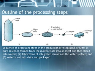
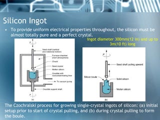
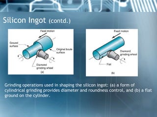
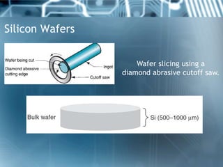
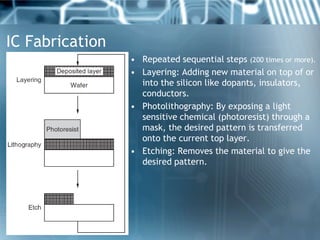
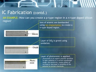
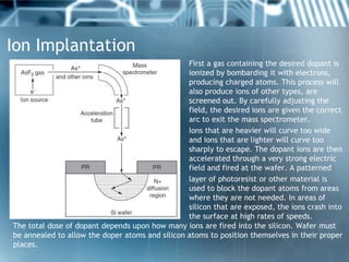
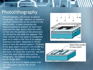
SlideShare a Scribd company logo
Manufacturing of Microprocessor
        Farooq Ahmad Shah
Preliminary Discussion
• Integrated circuit: An electronic circuit designed to perform some
  function, in which the electronic components (transistors, resistors,
  diodes, capacitors, etc.) are miniaturized, built into a small "chip" made
  of silicon and interconnected through tiny strands of aluminum. More
  commonly referred to as "microchips", or "IC chips―
• The chip found inside of a "musical" birthday card contain only a few
  dozen components, whereas a Pentium processor today contains over 800
  million transistors! When an integrated circuit is extremely complex, it
  is usually known as a microprocessor.
Preliminary Discussion                             (contd.)


 • Microprocessors are manufactured in clean rooms, the ambiance of which
   cleaner than a hospital operating room.
    –   The air in the clean room is air conditioned to a temperature of 21C (70F) and 45%
        relative humidity.
    –   The air is passed through a high-efficiency particulate air (HEPA) filter to capture particle
        contaminants
    –   workers must be covered from head to toe in specialized garments, called bunny suits,
        designed to trap particles.
Outline of the processing steps


Sequence of processing steps in the production of integrated circuits: (1)
pure silicon is formed from the molten state into an ingot and then sliced
into wafers; (2) fabrication of integrated circuits on the wafer surface; and
(3) wafer is cut into chips and packaged.
Silicon Ingot
• To provide uniform electrical properties throughout, the silicon must be
  almost totally pure and a perfect crystal.
                                           Ingot diameter 300mm(12 in) and up to
                                                       3m(10 ft) long


The Czochralski process for growing single-crystal ingots of silicon: (a) initial
setup prior to start of crystal pulling, and (b) during crystal pulling to form
the boule.
Silicon Ingot         (contd.)


Grinding operations used in shaping the silicon ingot: (a) a form of
cylindrical grinding provides diameter and roundness control, and (b) a flat
ground on the cylinder.
Silicon Wafers


                     Wafer slicing using a
                 diamond abrasive cutoff saw.
Silicon Wafers (contd.)


Two of the steps in wafer preparation: (a) contour grinding to round the
wafer rim, and (b) surface polishing.
IC Fabrication
                 • Repeated sequential steps (200 times or more).
                 • Layering: Adding new material on top of or
                   into the silicon like dopants, insulators,
                   conductors.
                 • Photolithography: By exposing a light
                   sensitive chemical (photoresist) through a
                   mask, the desired pattern is transferred
                   onto the current top layer.
                 • Etching: Removes the material to give the
                   desired pattern.
IC Fabrication (contd.)
AN EXAMPLE: How can you create a p-type region in a n-type doped silicon
region?                    Ions of arsenic are bombarded
                             using ion implantation to create a
                             n-type doped region.


                              Layer of SiO2 is grown using
                              oxidation.


                              Layer of photoresist is applied.
                              • photoresist is an organic polymer sensitive
                                to light radiation in a certain wavelength
                                range; the sensitivity causes either an
                                increase or decrease in solubility of the
                                polymer to certain chemicals.
IC Fabrication (E.g. contd.)
                         Expose photoresist using
                         appropriate lithographic mask.


                      Develop the photoresist.


                      Etch photoresist and silicon
                      dioxide.


                         Implant boron


                Remove silicon dioxide
IC Fabrication (contd.)


(A) A p-type wafer (silicon doped with Boron) has a epilayer of n-type (silicon doped with Phosphorous or
Arsenic)
(B) A mask is used to implant Silicon Dioxide, for the insulator
(C) Acceptor atoms (Boron) are diffused into the window in the Silicon Dioxide
(D) Using another mask additional Silicon Dioxide is grown. and donor atoms (elements like Arsenic with
excess electrons) are implanted.
(E) Another mask is used to grow additional Silicon Dioxide. Another mask is then used to implant
evaporated Aluminum or Copper for the contacts. This is a Bipolar Junction Transistor (BJT).
Packaging
• Wafer Testing: a computer-controlled needle probes contacts the chip
  connection pads and a series of DC tests are carried out to indicate short
  circuits and other faults; the failed chips are marked with an ink dot;
  these defects are not packaged.
• Chip Separation: A thin diamond-impregnated saw blade is used to
  perform the cutting operation. The sawing machine is highly automatic
  and its alignment with the ‘‘streets’’ between circuits is very accurate.
• Die Bonding: Automated handling systems pick the separated chips and
  place them for on the die. Epoxy is applied to the base of the chip.
• Wire Bonding After the die is bonded to the package, electrical
  connections are made between the contact pads on the chip surface and
  the package leads.

• Video
Thank you.
Ion Implantation
                                                 First a gas containing the desired dopant is
                                                 ionized by bombarding it with electrons,
                                                 producing charged atoms. This process will
                                                 also produce ions of other types, are
                                                 screened out. By carefully adjusting the
                                                 field, the desired ions are given the correct
                                                 arc to exit the mass spectrometer.
                                                 Ions that are heavier will curve too wide
                                                 and ions that are lighter will curve too
                                                 sharply to escape. The dopant ions are then
                                                 accelerated through a very strong electric
                                                 field and fired at the wafer. A patterned
                                                 layer of photoresist or other material is
                                                 used to block the dopant atoms from areas
                                                 where they are not needed. In areas of
                                                 silicon that are exposed, the ions crash into
                                                 the surface at high rates of speeds.
The total dose of dopant depends upon how many ions are fired into the silicon. Wafer must
be annealed to allow the doper atoms and silicon atoms to position themselves in their proper
places.
Photolithography
Photolithography, also known as optical
lithography, uses light radiation to expose a
coating of photoresist on the surface of the
silicon wafer; a mask containing the
required geometric pattern for each layer
separates the light source from the wafer,
so that only the portions of the photoresist
not blocked by the mask are exposed. The
mask consists of a flat plate of transparent
glass on to which a thin film of an opaque
substance has been deposited in certain
areas to form the desired pattern. Thickness
of the glass plate is around 2 mm (0.080 in),
whereas the deposited film is only a few
mm thick—for some film materials, less than
1 mm.The mask itself is fabricated by
lithography, the pattern being based on
circuit design data,
usually in the form of digital output from
the CAD system used by the circuit
designer.
Etching
Etching is usually done selectively, by coating surface areas that are to be protected
and leaving other areas exposed for etching. The coating maybe
an etch-resistant photoresist, or it maybe a previously applied layer of material such
as silicon dioxide.
Wet Chemical Etching involves the use of an aqueous solution, usually an acid, to
etch away a target material. The etching solution is selected because it chemically
attacks the specific material to be removed and not the protective layer used as a
mask.
Dry Plasma Etching uses an ionized gas to etch a target material. The ionized gas is
created by introducing an appropriate gas mixture into a vacuum chamber. and using
radio frequency (RF) electrical energy to ionize a portion of the gas, thus creating
a plasma. The high-energy plasma reacts with the target surface, vaporizing the
material to
remove it.
Manufacturing of microprocessor

More Related Content

What's hot

IC Fabrication Process
IC Fabrication ProcessIC Fabrication Process
IC Fabrication Process
Soudip Sinha Roy
 
【Junior新趨勢_先進封裝】
【Junior新趨勢_先進封裝】【Junior新趨勢_先進封裝】
【Junior新趨勢_先進封裝】
Collaborator
 
packaging types
packaging typespackaging types
packaging types
ahmed usama
 
Vlsi design and fabrication ppt
Vlsi design and fabrication  pptVlsi design and fabrication  ppt
Vlsi design and fabrication pptManjushree Mashal
 
High-end Performance Packaging 2020
High-end Performance Packaging 2020High-end Performance Packaging 2020
High-end Performance Packaging 2020
Yole Developpement
 
Wafer manufacturing process
Wafer manufacturing processWafer manufacturing process
Wafer manufacturing processadi mandloi
 
2.5D / 3D TSV & Wafer-Level Stacking: Technology & Market Updates 2019 Report...
2.5D / 3D TSV & Wafer-Level Stacking: Technology & Market Updates 2019 Report...2.5D / 3D TSV & Wafer-Level Stacking: Technology & Market Updates 2019 Report...
2.5D / 3D TSV & Wafer-Level Stacking: Technology & Market Updates 2019 Report...
Yole Developpement
 
VLSI Technology Trends
VLSI Technology TrendsVLSI Technology Trends
VLSI Technology Trends
Usha Mehta
 
Process of Semiconductor Manufacturing
Process of Semiconductor ManufacturingProcess of Semiconductor Manufacturing
Process of Semiconductor Manufacturing
WAFER WORLD, INC
 
Wafer Fabrication, CZ Method--ABU SYED KUET
Wafer Fabrication, CZ Method--ABU SYED KUETWafer Fabrication, CZ Method--ABU SYED KUET
Wafer Fabrication, CZ Method--ABU SYED KUET
A. S. M. Jannatul Islam
 
Easiest Monolithic 3D IC
Easiest Monolithic 3D ICEasiest Monolithic 3D IC
Easiest Monolithic 3D IC
Zvi Or-Bach
 
Lecture 8
Lecture 8Lecture 8
Lecture 8
avocado1111
 
OVERVIEW OF IC PACKAGING
OVERVIEW OF IC PACKAGINGOVERVIEW OF IC PACKAGING
OVERVIEW OF IC PACKAGING
Basavaraj Gangur
 
3dchips
3dchips3dchips
3dchips
MarkClemens
 
Etching, Diffusion, Ion Implantation--ABU SYED KUET
Etching, Diffusion, Ion Implantation--ABU SYED KUETEtching, Diffusion, Ion Implantation--ABU SYED KUET
Etching, Diffusion, Ion Implantation--ABU SYED KUET
A. S. M. Jannatul Islam
 
3DIC & 2,5D TSV Interconnect trends 2014 Kinsale Presentation Yole Developpement
3DIC & 2,5D TSV Interconnect trends 2014 Kinsale Presentation Yole Developpement3DIC & 2,5D TSV Interconnect trends 2014 Kinsale Presentation Yole Developpement
3DIC & 2,5D TSV Interconnect trends 2014 Kinsale Presentation Yole Developpement
Yole Developpement
 
Silicon on Insulator (SOI) Technology
Silicon on Insulator (SOI) TechnologySilicon on Insulator (SOI) Technology
Silicon on Insulator (SOI) Technology
Sudhanshu Janwadkar
 
Ic 封裝新技術發展趨勢
Ic 封裝新技術發展趨勢Ic 封裝新技術發展趨勢
Ic 封裝新技術發展趨勢
Kent Yang
 
Packaging of vlsi devices
Packaging of vlsi devicesPackaging of vlsi devices
Packaging of vlsi devicesAshu0711
 

What's hot (20)

IC Fabrication Process
IC Fabrication ProcessIC Fabrication Process
IC Fabrication Process
 
【Junior新趨勢_先進封裝】
【Junior新趨勢_先進封裝】【Junior新趨勢_先進封裝】
【Junior新趨勢_先進封裝】
 
packaging types
packaging typespackaging types
packaging types
 
Vlsi design and fabrication ppt
Vlsi design and fabrication  pptVlsi design and fabrication  ppt
Vlsi design and fabrication ppt
 
High-end Performance Packaging 2020
High-end Performance Packaging 2020High-end Performance Packaging 2020
High-end Performance Packaging 2020
 
Wafer manufacturing process
Wafer manufacturing processWafer manufacturing process
Wafer manufacturing process
 
2.5D / 3D TSV & Wafer-Level Stacking: Technology & Market Updates 2019 Report...
2.5D / 3D TSV & Wafer-Level Stacking: Technology & Market Updates 2019 Report...2.5D / 3D TSV & Wafer-Level Stacking: Technology & Market Updates 2019 Report...
2.5D / 3D TSV & Wafer-Level Stacking: Technology & Market Updates 2019 Report...
 
VLSI Technology Trends
VLSI Technology TrendsVLSI Technology Trends
VLSI Technology Trends
 
Process of Semiconductor Manufacturing
Process of Semiconductor ManufacturingProcess of Semiconductor Manufacturing
Process of Semiconductor Manufacturing
 
Fabrication of IC
Fabrication of ICFabrication of IC
Fabrication of IC
 
Wafer Fabrication, CZ Method--ABU SYED KUET
Wafer Fabrication, CZ Method--ABU SYED KUETWafer Fabrication, CZ Method--ABU SYED KUET
Wafer Fabrication, CZ Method--ABU SYED KUET
 
Easiest Monolithic 3D IC
Easiest Monolithic 3D ICEasiest Monolithic 3D IC
Easiest Monolithic 3D IC
 
Lecture 8
Lecture 8Lecture 8
Lecture 8
 
OVERVIEW OF IC PACKAGING
OVERVIEW OF IC PACKAGINGOVERVIEW OF IC PACKAGING
OVERVIEW OF IC PACKAGING
 
3dchips
3dchips3dchips
3dchips
 
Etching, Diffusion, Ion Implantation--ABU SYED KUET
Etching, Diffusion, Ion Implantation--ABU SYED KUETEtching, Diffusion, Ion Implantation--ABU SYED KUET
Etching, Diffusion, Ion Implantation--ABU SYED KUET
 
3DIC & 2,5D TSV Interconnect trends 2014 Kinsale Presentation Yole Developpement
3DIC & 2,5D TSV Interconnect trends 2014 Kinsale Presentation Yole Developpement3DIC & 2,5D TSV Interconnect trends 2014 Kinsale Presentation Yole Developpement
3DIC & 2,5D TSV Interconnect trends 2014 Kinsale Presentation Yole Developpement
 
Silicon on Insulator (SOI) Technology
Silicon on Insulator (SOI) TechnologySilicon on Insulator (SOI) Technology
Silicon on Insulator (SOI) Technology
 
Ic 封裝新技術發展趨勢
Ic 封裝新技術發展趨勢Ic 封裝新技術發展趨勢
Ic 封裝新技術發展趨勢
 
Packaging of vlsi devices
Packaging of vlsi devicesPackaging of vlsi devices
Packaging of vlsi devices
 

Viewers also liked

Making of a silicon chip
Making of a silicon chipMaking of a silicon chip
Making of a silicon chipsurabhi8
 
Evolution Of Microprocessors
Evolution Of MicroprocessorsEvolution Of Microprocessors
Evolution Of Microprocessors
harinder
 
Lecture 2 ic fabrication processing & wafer preparation
Lecture 2 ic fabrication processing & wafer preparationLecture 2 ic fabrication processing & wafer preparation
Lecture 2 ic fabrication processing & wafer preparationDr. Ghanshyam Singh
 
From Sand to Silicon“Making of a Chip”
From Sand to Silicon“Making of a Chip”From Sand to Silicon“Making of a Chip”
From Sand to Silicon“Making of a Chip”
Gautham Rajesh
 
Applications of microprocessor
Applications of microprocessorApplications of microprocessor
Applications of microprocessor
Anjali Agrawal
 
3. crystal growth and wafer fabrication
3. crystal growth and wafer fabrication3. crystal growth and wafer fabrication
3. crystal growth and wafer fabrication
Bhargav Veepuri
 
Round cycle flow chart 6 stages powerpoint templates 0712
Round cycle flow chart 6 stages powerpoint templates 0712Round cycle flow chart 6 stages powerpoint templates 0712
Round cycle flow chart 6 stages powerpoint templates 0712SlideTeam.net
 
microprocessor
microprocessormicroprocessor
microprocessorillpa
 
Micro Processor Mini Project,Electronic Quiz Table
Micro Processor Mini Project,Electronic Quiz TableMicro Processor Mini Project,Electronic Quiz Table
Micro Processor Mini Project,Electronic Quiz Table
Subhashini Sundaram
 
INTEGRATED CIRCUIT
INTEGRATED CIRCUITINTEGRATED CIRCUIT
INTEGRATED CIRCUIT
Sripati Mahapatra
 
Crystal growth
Crystal growthCrystal growth
Crystal growth
Rishi Kumar Jha
 
Photonic Integrated Circuit Technology
Photonic Integrated Circuit TechnologyPhotonic Integrated Circuit Technology
Photonic Integrated Circuit Technology
Rinu Antony
 
3D IC Presented by Tripti Kumari, School of Engineering, CUSAT
3D IC Presented by Tripti Kumari, School of Engineering, CUSAT3D IC Presented by Tripti Kumari, School of Engineering, CUSAT
3D IC Presented by Tripti Kumari, School of Engineering, CUSAT
thevijayps
 
Laser diode fabrication
Laser diode fabricationLaser diode fabrication
Laser diode fabrication
uttam999
 
Cpu presentation
Cpu presentationCpu presentation
Cpu presentationHarry Singh
 
Evolution Of Microprocessor
Evolution Of MicroprocessorEvolution Of Microprocessor
Evolution Of Microprocessor
guest3870d0
 
Microprocessor ppt
Microprocessor pptMicroprocessor ppt
Microprocessor ppt
swaminath kanhere
 
Process flow chart 6 stages powerpoint templates 0712
Process flow chart 6 stages powerpoint templates 0712Process flow chart 6 stages powerpoint templates 0712
Process flow chart 6 stages powerpoint templates 0712SlideTeam.net
 
Motherboard and its components
Motherboard and its componentsMotherboard and its components
Motherboard and its components
Jishnu Pradeep
 

Viewers also liked (20)

Making of a silicon chip
Making of a silicon chipMaking of a silicon chip
Making of a silicon chip
 
Evolution Of Microprocessors
Evolution Of MicroprocessorsEvolution Of Microprocessors
Evolution Of Microprocessors
 
Lecture 2 ic fabrication processing & wafer preparation
Lecture 2 ic fabrication processing & wafer preparationLecture 2 ic fabrication processing & wafer preparation
Lecture 2 ic fabrication processing & wafer preparation
 
From Sand to Silicon“Making of a Chip”
From Sand to Silicon“Making of a Chip”From Sand to Silicon“Making of a Chip”
From Sand to Silicon“Making of a Chip”
 
Applications of microprocessor
Applications of microprocessorApplications of microprocessor
Applications of microprocessor
 
3. crystal growth and wafer fabrication
3. crystal growth and wafer fabrication3. crystal growth and wafer fabrication
3. crystal growth and wafer fabrication
 
Micro controller & Micro processor
Micro controller & Micro processorMicro controller & Micro processor
Micro controller & Micro processor
 
Round cycle flow chart 6 stages powerpoint templates 0712
Round cycle flow chart 6 stages powerpoint templates 0712Round cycle flow chart 6 stages powerpoint templates 0712
Round cycle flow chart 6 stages powerpoint templates 0712
 
microprocessor
microprocessormicroprocessor
microprocessor
 
Micro Processor Mini Project,Electronic Quiz Table
Micro Processor Mini Project,Electronic Quiz TableMicro Processor Mini Project,Electronic Quiz Table
Micro Processor Mini Project,Electronic Quiz Table
 
INTEGRATED CIRCUIT
INTEGRATED CIRCUITINTEGRATED CIRCUIT
INTEGRATED CIRCUIT
 
Crystal growth
Crystal growthCrystal growth
Crystal growth
 
Photonic Integrated Circuit Technology
Photonic Integrated Circuit TechnologyPhotonic Integrated Circuit Technology
Photonic Integrated Circuit Technology
 
3D IC Presented by Tripti Kumari, School of Engineering, CUSAT
3D IC Presented by Tripti Kumari, School of Engineering, CUSAT3D IC Presented by Tripti Kumari, School of Engineering, CUSAT
3D IC Presented by Tripti Kumari, School of Engineering, CUSAT
 
Laser diode fabrication
Laser diode fabricationLaser diode fabrication
Laser diode fabrication
 
Cpu presentation
Cpu presentationCpu presentation
Cpu presentation
 
Evolution Of Microprocessor
Evolution Of MicroprocessorEvolution Of Microprocessor
Evolution Of Microprocessor
 
Microprocessor ppt
Microprocessor pptMicroprocessor ppt
Microprocessor ppt
 
Process flow chart 6 stages powerpoint templates 0712
Process flow chart 6 stages powerpoint templates 0712Process flow chart 6 stages powerpoint templates 0712
Process flow chart 6 stages powerpoint templates 0712
 
Motherboard and its components
Motherboard and its componentsMotherboard and its components
Motherboard and its components
 

Similar to Manufacturing of microprocessor

MONOLITHIC IC PROCESSES ppt.pptx
MONOLITHIC IC PROCESSES ppt.pptxMONOLITHIC IC PROCESSES ppt.pptx
MONOLITHIC IC PROCESSES ppt.pptx
ParasSingh894545
 
integrated circuit febrication
integrated circuit febricationintegrated circuit febrication
integrated circuit febrication
sky lark
 
Fabrication steps of IC
Fabrication steps of ICFabrication steps of IC
Fabrication steps of IC
Gowri Kishore
 
Monolithic implementation of parasitic elements
Monolithic implementation of parasitic elementsMonolithic implementation of parasitic elements
Monolithic implementation of parasitic elements
GOPICHAND NAGUBOINA
 
Fabrication process of Integrated Circuit (IC's)
Fabrication process of Integrated Circuit (IC's)Fabrication process of Integrated Circuit (IC's)
Fabrication process of Integrated Circuit (IC's)
COMSATS Abbottabad
 
vlsi fabrication
vlsi fabricationvlsi fabrication
vlsi fabrication
Srikanth Vas
 
Chapter 1-IC Fabrication.pptx
Chapter 1-IC Fabrication.pptxChapter 1-IC Fabrication.pptx
Chapter 1-IC Fabrication.pptx
Karthik Prof.
 
Integrated Circuits
Integrated CircuitsIntegrated Circuits
Integrated Circuits
ANAND G
 
Epitaxial growth
Epitaxial growthEpitaxial growth
Epitaxial growth
IYPUMANI
 
Photonic Materials
Photonic MaterialsPhotonic Materials
Photonic Materials
Gaurav Singh Chandel
 
Optical fiber laser
Optical fiber laser Optical fiber laser
Optical fiber laser
Monalisa Mallick
 
Solar cells fabrication and surface processing
Solar cells fabrication and surface processingSolar cells fabrication and surface processing
Solar cells fabrication and surface processing
Chandan
 
microfabrication-180118174836 (1).pdf
microfabrication-180118174836 (1).pdfmicrofabrication-180118174836 (1).pdf
microfabrication-180118174836 (1).pdf
Senguttuvan Nagarajan
 
MOSFET(ABOUT,FABRICATION)
MOSFET(ABOUT,FABRICATION)MOSFET(ABOUT,FABRICATION)
MOSFET(ABOUT,FABRICATION)
HARSHIT SONI
 
Intel Chip , How do they do It
Intel Chip , How do they do ItIntel Chip , How do they do It
Intel Chip , How do they do It
parekhjigarh
 
Processors Manufacturing Technology By Dr Islam Salama.pdf
Processors Manufacturing Technology By Dr Islam Salama.pdfProcessors Manufacturing Technology By Dr Islam Salama.pdf
Processors Manufacturing Technology By Dr Islam Salama.pdf
Dr-Islam Salama
 
Ion Implantation UPS.pdf
Ion Implantation UPS.pdfIon Implantation UPS.pdf
Ion Implantation UPS.pdf
ssuser0e2fb9
 
Vlsi assembly technology
Vlsi  assembly technologyVlsi  assembly technology
Vlsi assembly technologyAshu0711
 

Similar to Manufacturing of microprocessor (20)

MONOLITHIC IC PROCESSES ppt.pptx
MONOLITHIC IC PROCESSES ppt.pptxMONOLITHIC IC PROCESSES ppt.pptx
MONOLITHIC IC PROCESSES ppt.pptx
 
integrated circuit febrication
integrated circuit febricationintegrated circuit febrication
integrated circuit febrication
 
Fabrication steps of IC
Fabrication steps of ICFabrication steps of IC
Fabrication steps of IC
 
Ic fab
Ic fabIc fab
Ic fab
 
Monolithic implementation of parasitic elements
Monolithic implementation of parasitic elementsMonolithic implementation of parasitic elements
Monolithic implementation of parasitic elements
 
Fabrication process of Integrated Circuit (IC's)
Fabrication process of Integrated Circuit (IC's)Fabrication process of Integrated Circuit (IC's)
Fabrication process of Integrated Circuit (IC's)
 
vlsi fabrication
vlsi fabricationvlsi fabrication
vlsi fabrication
 
Chapter 1-IC Fabrication.pptx
Chapter 1-IC Fabrication.pptxChapter 1-IC Fabrication.pptx
Chapter 1-IC Fabrication.pptx
 
Integrated Circuits
Integrated CircuitsIntegrated Circuits
Integrated Circuits
 
integratedcircuits
integratedcircuitsintegratedcircuits
integratedcircuits
 
Epitaxial growth
Epitaxial growthEpitaxial growth
Epitaxial growth
 
Photonic Materials
Photonic MaterialsPhotonic Materials
Photonic Materials
 
Optical fiber laser
Optical fiber laser Optical fiber laser
Optical fiber laser
 
Solar cells fabrication and surface processing
Solar cells fabrication and surface processingSolar cells fabrication and surface processing
Solar cells fabrication and surface processing
 
microfabrication-180118174836 (1).pdf
microfabrication-180118174836 (1).pdfmicrofabrication-180118174836 (1).pdf
microfabrication-180118174836 (1).pdf
 
MOSFET(ABOUT,FABRICATION)
MOSFET(ABOUT,FABRICATION)MOSFET(ABOUT,FABRICATION)
MOSFET(ABOUT,FABRICATION)
 
Intel Chip , How do they do It
Intel Chip , How do they do ItIntel Chip , How do they do It
Intel Chip , How do they do It
 
Processors Manufacturing Technology By Dr Islam Salama.pdf
Processors Manufacturing Technology By Dr Islam Salama.pdfProcessors Manufacturing Technology By Dr Islam Salama.pdf
Processors Manufacturing Technology By Dr Islam Salama.pdf
 
Ion Implantation UPS.pdf
Ion Implantation UPS.pdfIon Implantation UPS.pdf
Ion Implantation UPS.pdf
 
Vlsi assembly technology
Vlsi  assembly technologyVlsi  assembly technology
Vlsi assembly technology
 

Recently uploaded

Premium MEAN Stack Development Solutions for Modern Businesses
Premium MEAN Stack Development Solutions for Modern BusinessesPremium MEAN Stack Development Solutions for Modern Businesses
Premium MEAN Stack Development Solutions for Modern Businesses
SynapseIndia
 
FINAL PRESENTATION.pptx12143241324134134
FINAL PRESENTATION.pptx12143241324134134FINAL PRESENTATION.pptx12143241324134134
FINAL PRESENTATION.pptx12143241324134134
LR1709MUSIC
 
3.0 Project 2_ Developing My Brand Identity Kit.pptx
3.0 Project 2_ Developing My Brand Identity Kit.pptx3.0 Project 2_ Developing My Brand Identity Kit.pptx
3.0 Project 2_ Developing My Brand Identity Kit.pptx
tanyjahb
 
5 Things You Need To Know Before Hiring a Videographer
5 Things You Need To Know Before Hiring a Videographer5 Things You Need To Know Before Hiring a Videographer
5 Things You Need To Know Before Hiring a Videographer
ofm712785
 
What are the main advantages of using HR recruiter services.pdf
What are the main advantages of using HR recruiter services.pdfWhat are the main advantages of using HR recruiter services.pdf
What are the main advantages of using HR recruiter services.pdf
HumanResourceDimensi1
 
Search Disrupted Google’s Leaked Documents Rock the SEO World.pdf
Search Disrupted Google’s Leaked Documents Rock the SEO World.pdfSearch Disrupted Google’s Leaked Documents Rock the SEO World.pdf
Search Disrupted Google’s Leaked Documents Rock the SEO World.pdf
Arihant Webtech Pvt. Ltd
 
PriyoShop Celebration Pohela Falgun Mar 20, 2024
PriyoShop Celebration Pohela Falgun Mar 20, 2024PriyoShop Celebration Pohela Falgun Mar 20, 2024
PriyoShop Celebration Pohela Falgun Mar 20, 2024
PriyoShop.com LTD
 
Sustainability: Balancing the Environment, Equity & Economy
Sustainability: Balancing the Environment, Equity & EconomySustainability: Balancing the Environment, Equity & Economy
Sustainability: Balancing the Environment, Equity & Economy
Operational Excellence Consulting
 
India Orthopedic Devices Market: Unlocking Growth Secrets, Trends and Develop...
India Orthopedic Devices Market: Unlocking Growth Secrets, Trends and Develop...India Orthopedic Devices Market: Unlocking Growth Secrets, Trends and Develop...
India Orthopedic Devices Market: Unlocking Growth Secrets, Trends and Develop...
Kumar Satyam
 
Meas_Dylan_DMBS_PB1_2024-05XX_Revised.pdf
Meas_Dylan_DMBS_PB1_2024-05XX_Revised.pdfMeas_Dylan_DMBS_PB1_2024-05XX_Revised.pdf
Meas_Dylan_DMBS_PB1_2024-05XX_Revised.pdf
dylandmeas
 
Cracking the Workplace Discipline Code Main.pptx
Cracking the Workplace Discipline Code Main.pptxCracking the Workplace Discipline Code Main.pptx
Cracking the Workplace Discipline Code Main.pptx
Workforce Group
 
chapter 10 - excise tax of transfer and business taxation
chapter 10 - excise tax of transfer and business taxationchapter 10 - excise tax of transfer and business taxation
chapter 10 - excise tax of transfer and business taxation
AUDIJEAngelo
 
20240425_ TJ Communications Credentials_compressed.pdf
20240425_ TJ Communications Credentials_compressed.pdf20240425_ TJ Communications Credentials_compressed.pdf
20240425_ TJ Communications Credentials_compressed.pdf
tjcomstrang
 
BeMetals Presentation_May_22_2024 .pdf
BeMetals Presentation_May_22_2024   .pdfBeMetals Presentation_May_22_2024   .pdf
BeMetals Presentation_May_22_2024 .pdf
DerekIwanaka1
 
一比一原版加拿大渥太华大学毕业证(uottawa毕业证书)如何办理
一比一原版加拿大渥太华大学毕业证(uottawa毕业证书)如何办理一比一原版加拿大渥太华大学毕业证(uottawa毕业证书)如何办理
一比一原版加拿大渥太华大学毕业证(uottawa毕业证书)如何办理
taqyed
 
Maksym Vyshnivetskyi: PMO Quality Management (UA)
Maksym Vyshnivetskyi: PMO Quality Management (UA)Maksym Vyshnivetskyi: PMO Quality Management (UA)
Maksym Vyshnivetskyi: PMO Quality Management (UA)
Lviv Startup Club
 
What is the TDS Return Filing Due Date for FY 2024-25.pdf
What is the TDS Return Filing Due Date for FY 2024-25.pdfWhat is the TDS Return Filing Due Date for FY 2024-25.pdf
What is the TDS Return Filing Due Date for FY 2024-25.pdf
seoforlegalpillers
 
The-McKinsey-7S-Framework. strategic management
The-McKinsey-7S-Framework. strategic managementThe-McKinsey-7S-Framework. strategic management
The-McKinsey-7S-Framework. strategic management
Bojamma2
 
Skye Residences | Extended Stay Residences Near Toronto Airport
Skye Residences | Extended Stay Residences Near Toronto AirportSkye Residences | Extended Stay Residences Near Toronto Airport
Skye Residences | Extended Stay Residences Near Toronto Airport
marketingjdass
 
Introduction to Amazon company 111111111111
Introduction to Amazon company 111111111111Introduction to Amazon company 111111111111
Introduction to Amazon company 111111111111
zoyaansari11365
 

Recently uploaded (20)

Premium MEAN Stack Development Solutions for Modern Businesses
Premium MEAN Stack Development Solutions for Modern BusinessesPremium MEAN Stack Development Solutions for Modern Businesses
Premium MEAN Stack Development Solutions for Modern Businesses
 
FINAL PRESENTATION.pptx12143241324134134
FINAL PRESENTATION.pptx12143241324134134FINAL PRESENTATION.pptx12143241324134134
FINAL PRESENTATION.pptx12143241324134134
 
3.0 Project 2_ Developing My Brand Identity Kit.pptx
3.0 Project 2_ Developing My Brand Identity Kit.pptx3.0 Project 2_ Developing My Brand Identity Kit.pptx
3.0 Project 2_ Developing My Brand Identity Kit.pptx
 
5 Things You Need To Know Before Hiring a Videographer
5 Things You Need To Know Before Hiring a Videographer5 Things You Need To Know Before Hiring a Videographer
5 Things You Need To Know Before Hiring a Videographer
 
What are the main advantages of using HR recruiter services.pdf
What are the main advantages of using HR recruiter services.pdfWhat are the main advantages of using HR recruiter services.pdf
What are the main advantages of using HR recruiter services.pdf
 
Search Disrupted Google’s Leaked Documents Rock the SEO World.pdf
Search Disrupted Google’s Leaked Documents Rock the SEO World.pdfSearch Disrupted Google’s Leaked Documents Rock the SEO World.pdf
Search Disrupted Google’s Leaked Documents Rock the SEO World.pdf
 
PriyoShop Celebration Pohela Falgun Mar 20, 2024
PriyoShop Celebration Pohela Falgun Mar 20, 2024PriyoShop Celebration Pohela Falgun Mar 20, 2024
PriyoShop Celebration Pohela Falgun Mar 20, 2024
 
Sustainability: Balancing the Environment, Equity & Economy
Sustainability: Balancing the Environment, Equity & EconomySustainability: Balancing the Environment, Equity & Economy
Sustainability: Balancing the Environment, Equity & Economy
 
India Orthopedic Devices Market: Unlocking Growth Secrets, Trends and Develop...
India Orthopedic Devices Market: Unlocking Growth Secrets, Trends and Develop...India Orthopedic Devices Market: Unlocking Growth Secrets, Trends and Develop...
India Orthopedic Devices Market: Unlocking Growth Secrets, Trends and Develop...
 
Meas_Dylan_DMBS_PB1_2024-05XX_Revised.pdf
Meas_Dylan_DMBS_PB1_2024-05XX_Revised.pdfMeas_Dylan_DMBS_PB1_2024-05XX_Revised.pdf
Meas_Dylan_DMBS_PB1_2024-05XX_Revised.pdf
 
Cracking the Workplace Discipline Code Main.pptx
Cracking the Workplace Discipline Code Main.pptxCracking the Workplace Discipline Code Main.pptx
Cracking the Workplace Discipline Code Main.pptx
 
chapter 10 - excise tax of transfer and business taxation
chapter 10 - excise tax of transfer and business taxationchapter 10 - excise tax of transfer and business taxation
chapter 10 - excise tax of transfer and business taxation
 
20240425_ TJ Communications Credentials_compressed.pdf
20240425_ TJ Communications Credentials_compressed.pdf20240425_ TJ Communications Credentials_compressed.pdf
20240425_ TJ Communications Credentials_compressed.pdf
 
BeMetals Presentation_May_22_2024 .pdf
BeMetals Presentation_May_22_2024   .pdfBeMetals Presentation_May_22_2024   .pdf
BeMetals Presentation_May_22_2024 .pdf
 
一比一原版加拿大渥太华大学毕业证(uottawa毕业证书)如何办理
一比一原版加拿大渥太华大学毕业证(uottawa毕业证书)如何办理一比一原版加拿大渥太华大学毕业证(uottawa毕业证书)如何办理
一比一原版加拿大渥太华大学毕业证(uottawa毕业证书)如何办理
 
Maksym Vyshnivetskyi: PMO Quality Management (UA)
Maksym Vyshnivetskyi: PMO Quality Management (UA)Maksym Vyshnivetskyi: PMO Quality Management (UA)
Maksym Vyshnivetskyi: PMO Quality Management (UA)
 
What is the TDS Return Filing Due Date for FY 2024-25.pdf
What is the TDS Return Filing Due Date for FY 2024-25.pdfWhat is the TDS Return Filing Due Date for FY 2024-25.pdf
What is the TDS Return Filing Due Date for FY 2024-25.pdf
 
The-McKinsey-7S-Framework. strategic management
The-McKinsey-7S-Framework. strategic managementThe-McKinsey-7S-Framework. strategic management
The-McKinsey-7S-Framework. strategic management
 
Skye Residences | Extended Stay Residences Near Toronto Airport
Skye Residences | Extended Stay Residences Near Toronto AirportSkye Residences | Extended Stay Residences Near Toronto Airport
Skye Residences | Extended Stay Residences Near Toronto Airport
 
Introduction to Amazon company 111111111111
Introduction to Amazon company 111111111111Introduction to Amazon company 111111111111
Introduction to Amazon company 111111111111
 

Manufacturing of microprocessor

  • 2. Preliminary Discussion • Integrated circuit: An electronic circuit designed to perform some function, in which the electronic components (transistors, resistors, diodes, capacitors, etc.) are miniaturized, built into a small "chip" made of silicon and interconnected through tiny strands of aluminum. More commonly referred to as "microchips", or "IC chips― • The chip found inside of a "musical" birthday card contain only a few dozen components, whereas a Pentium processor today contains over 800 million transistors! When an integrated circuit is extremely complex, it is usually known as a microprocessor.
  • 3. Preliminary Discussion (contd.) • Microprocessors are manufactured in clean rooms, the ambiance of which cleaner than a hospital operating room. – The air in the clean room is air conditioned to a temperature of 21C (70F) and 45% relative humidity. – The air is passed through a high-efficiency particulate air (HEPA) filter to capture particle contaminants – workers must be covered from head to toe in specialized garments, called bunny suits, designed to trap particles.
  • 4. Outline of the processing steps Sequence of processing steps in the production of integrated circuits: (1) pure silicon is formed from the molten state into an ingot and then sliced into wafers; (2) fabrication of integrated circuits on the wafer surface; and (3) wafer is cut into chips and packaged.
  • 5. Silicon Ingot • To provide uniform electrical properties throughout, the silicon must be almost totally pure and a perfect crystal. Ingot diameter 300mm(12 in) and up to 3m(10 ft) long The Czochralski process for growing single-crystal ingots of silicon: (a) initial setup prior to start of crystal pulling, and (b) during crystal pulling to form the boule.
  • 6. Silicon Ingot (contd.) Grinding operations used in shaping the silicon ingot: (a) a form of cylindrical grinding provides diameter and roundness control, and (b) a flat ground on the cylinder.
  • 7. Silicon Wafers Wafer slicing using a diamond abrasive cutoff saw.
  • 8. Silicon Wafers (contd.) Two of the steps in wafer preparation: (a) contour grinding to round the wafer rim, and (b) surface polishing.
  • 9. IC Fabrication • Repeated sequential steps (200 times or more). • Layering: Adding new material on top of or into the silicon like dopants, insulators, conductors. • Photolithography: By exposing a light sensitive chemical (photoresist) through a mask, the desired pattern is transferred onto the current top layer. • Etching: Removes the material to give the desired pattern.
  • 10. IC Fabrication (contd.) AN EXAMPLE: How can you create a p-type region in a n-type doped silicon region? Ions of arsenic are bombarded using ion implantation to create a n-type doped region. Layer of SiO2 is grown using oxidation. Layer of photoresist is applied. • photoresist is an organic polymer sensitive to light radiation in a certain wavelength range; the sensitivity causes either an increase or decrease in solubility of the polymer to certain chemicals.
  • 11. IC Fabrication (E.g. contd.) Expose photoresist using appropriate lithographic mask. Develop the photoresist. Etch photoresist and silicon dioxide. Implant boron Remove silicon dioxide
  • 12. IC Fabrication (contd.) (A) A p-type wafer (silicon doped with Boron) has a epilayer of n-type (silicon doped with Phosphorous or Arsenic) (B) A mask is used to implant Silicon Dioxide, for the insulator (C) Acceptor atoms (Boron) are diffused into the window in the Silicon Dioxide (D) Using another mask additional Silicon Dioxide is grown. and donor atoms (elements like Arsenic with excess electrons) are implanted. (E) Another mask is used to grow additional Silicon Dioxide. Another mask is then used to implant evaporated Aluminum or Copper for the contacts. This is a Bipolar Junction Transistor (BJT).
  • 13. Packaging • Wafer Testing: a computer-controlled needle probes contacts the chip connection pads and a series of DC tests are carried out to indicate short circuits and other faults; the failed chips are marked with an ink dot; these defects are not packaged. • Chip Separation: A thin diamond-impregnated saw blade is used to perform the cutting operation. The sawing machine is highly automatic and its alignment with the ‘‘streets’’ between circuits is very accurate. • Die Bonding: Automated handling systems pick the separated chips and place them for on the die. Epoxy is applied to the base of the chip. • Wire Bonding After the die is bonded to the package, electrical connections are made between the contact pads on the chip surface and the package leads. • Video
  • 15. Ion Implantation First a gas containing the desired dopant is ionized by bombarding it with electrons, producing charged atoms. This process will also produce ions of other types, are screened out. By carefully adjusting the field, the desired ions are given the correct arc to exit the mass spectrometer. Ions that are heavier will curve too wide and ions that are lighter will curve too sharply to escape. The dopant ions are then accelerated through a very strong electric field and fired at the wafer. A patterned layer of photoresist or other material is used to block the dopant atoms from areas where they are not needed. In areas of silicon that are exposed, the ions crash into the surface at high rates of speeds. The total dose of dopant depends upon how many ions are fired into the silicon. Wafer must be annealed to allow the doper atoms and silicon atoms to position themselves in their proper places.
  • 16. Photolithography Photolithography, also known as optical lithography, uses light radiation to expose a coating of photoresist on the surface of the silicon wafer; a mask containing the required geometric pattern for each layer separates the light source from the wafer, so that only the portions of the photoresist not blocked by the mask are exposed. The mask consists of a flat plate of transparent glass on to which a thin film of an opaque substance has been deposited in certain areas to form the desired pattern. Thickness of the glass plate is around 2 mm (0.080 in), whereas the deposited film is only a few mm thick—for some film materials, less than 1 mm.The mask itself is fabricated by lithography, the pattern being based on circuit design data, usually in the form of digital output from the CAD system used by the circuit designer.
  • 17. Etching Etching is usually done selectively, by coating surface areas that are to be protected and leaving other areas exposed for etching. The coating maybe an etch-resistant photoresist, or it maybe a previously applied layer of material such as silicon dioxide. Wet Chemical Etching involves the use of an aqueous solution, usually an acid, to etch away a target material. The etching solution is selected because it chemically attacks the specific material to be removed and not the protective layer used as a mask. Dry Plasma Etching uses an ionized gas to etch a target material. The ionized gas is created by introducing an appropriate gas mixture into a vacuum chamber. and using radio frequency (RF) electrical energy to ionize a portion of the gas, thus creating a plasma. The high-energy plasma reacts with the target surface, vaporizing the material to remove it.