Downloaded 1,121 times
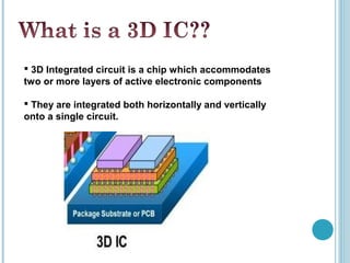
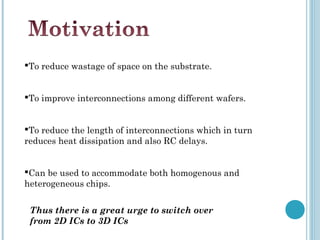
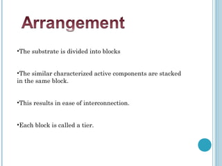
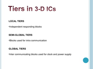
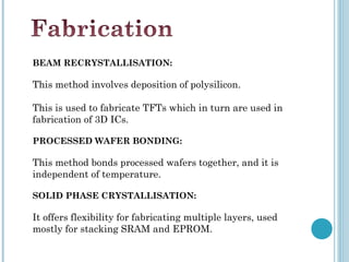

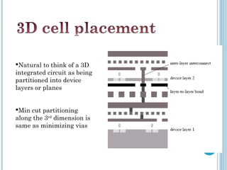
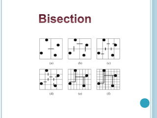
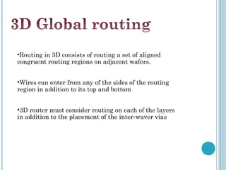
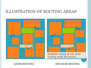


3D integrated circuits stack active electronic components in multiple layers within a single circuit to reduce wasted space and improve interconnectivity between components. This allows both homogenous and heterogeneous chips to be accommodated. The substrate is divided into tiers with similar components stacked together to ease interconnections. Fabrication methods include beam recrystallization, processed wafer bonding, and solid phase crystallization. Routing in 3D considers multiple layers and placement of inter-wafer vias to reduce delays. MAGIC layout editing software provides bonding commands to treat layered designs as single entities. 3D ICs provide significant improvements over conventional 2D designs.