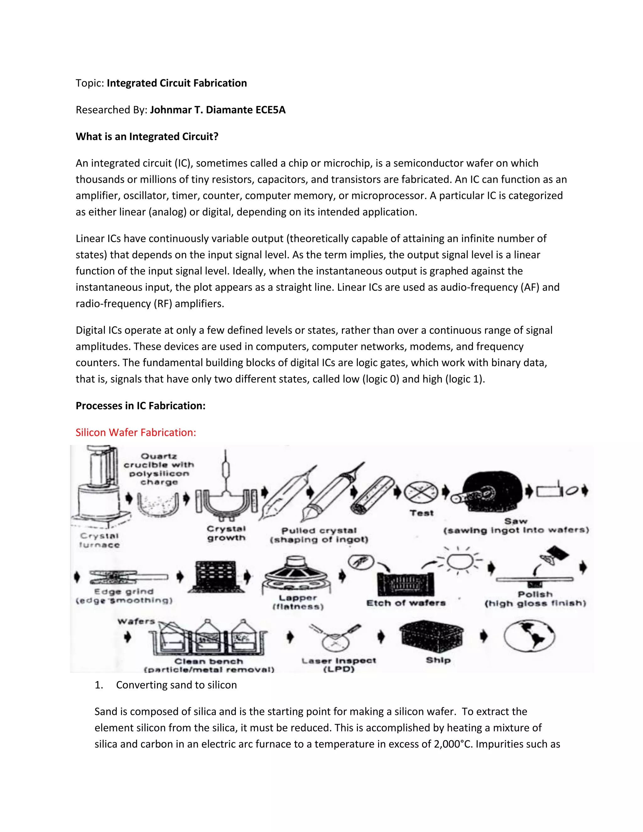
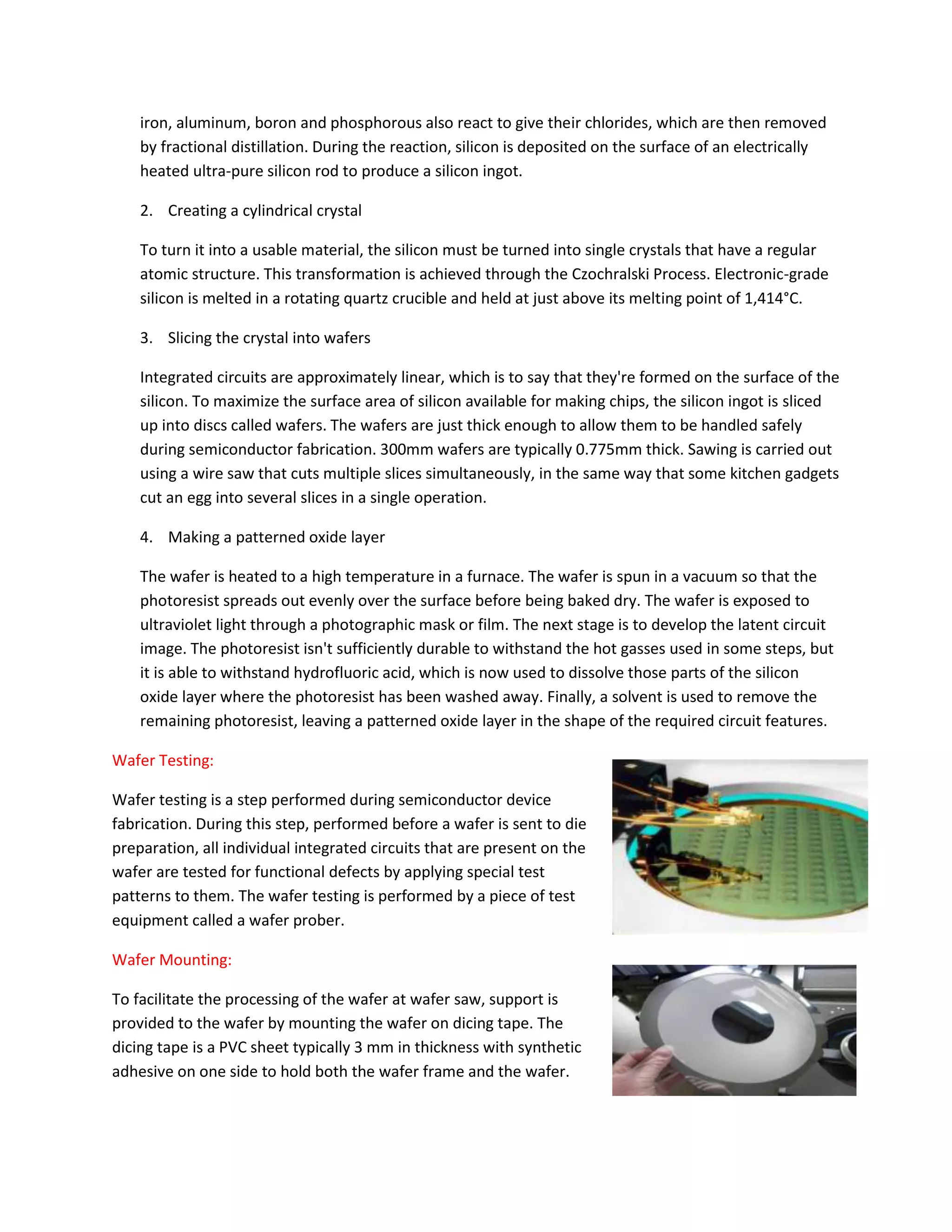
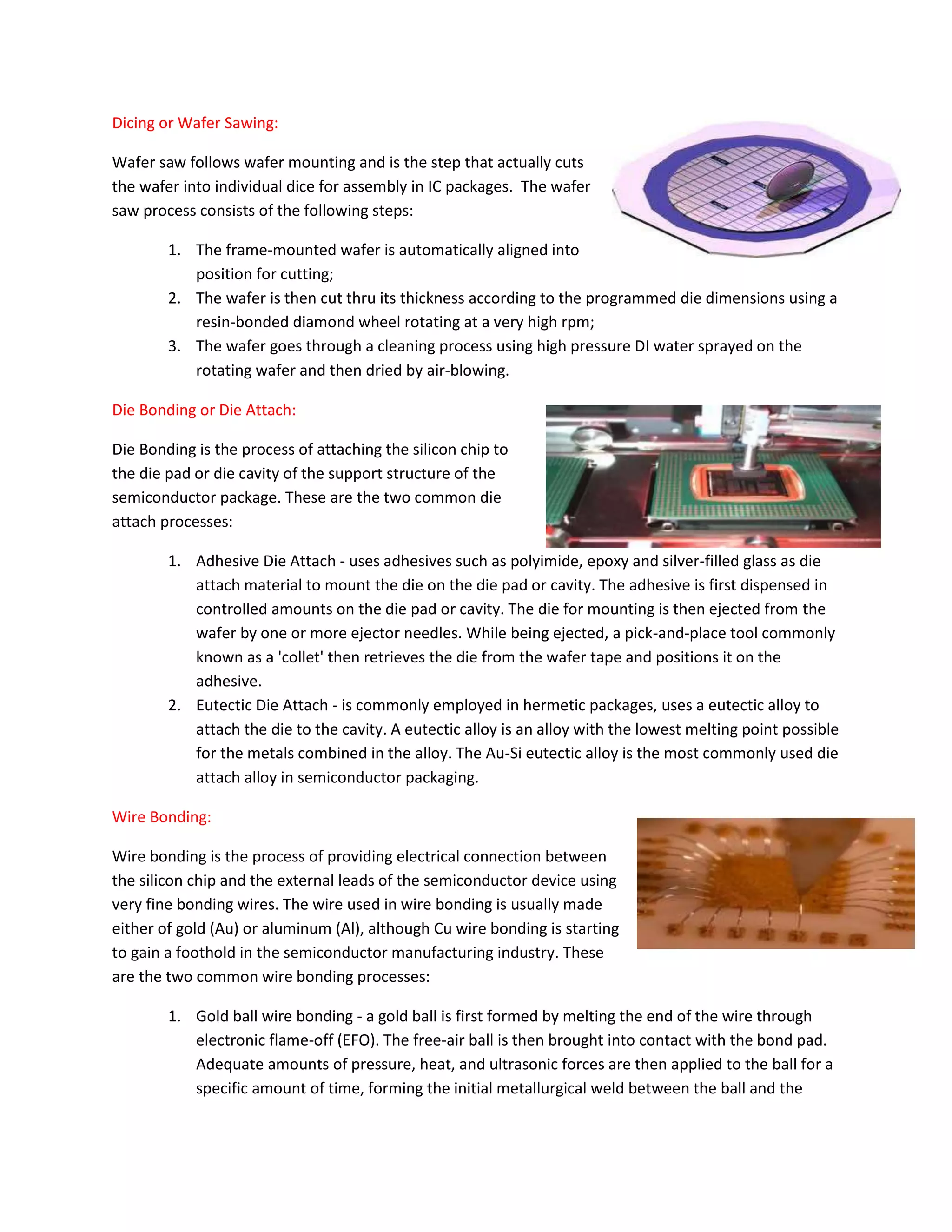
An integrated circuit is a semiconductor wafer containing thousands of tiny resistors, capacitors and transistors. There are several key steps in the fabrication of integrated circuits:
1. Silicon wafers are created by slicing purified silicon crystals into thin discs.
2. A patterned oxide layer is formed on the wafer through a photolithography process using a mask to transfer circuit patterns to the wafer.
3. The wafer then undergoes several post-processing steps like dicing, die bonding, wire bonding and encapsulation before electrical testing verifies its functioning.
Semiconductor device fabrication is the process used to create the integrated circuits that are present in everyday electrical and electronic devices. It is a multiple-step sequence of photo lithographic and chemical processing steps during which electronic circuits are gradually created on a wafer made of pure semiconducting material. Silicon is almost always used, but various compound semiconductors are used for specialized applications.
This is one of the fabrication technology used in IC fabrication. This technique is mostly used in flexible electronics. It contains various other subprocesses in it.
1.Silicon Manufacturing
a) Czochralski method.
b) Wafer Manufacturing
c) Crystal structure
2.Photolithography
a) Photoresists
b) Photomask and Reticles
c) Patterning
Semiconductors are materials that have electrical conductivity between conductors such as most metals and nonconductors or insulators like ceramics. How much electricity a semiconductor can conduct depends on the material and its mixture content.
Semiconductors can be insulators at low temperatures and conductors at high temperatures. As they are used in the fabrication of electronic devices, semiconductors play an important role in our lives.
EDC Unit-5 Introduction to Integrated Circuits (ICs) | RGPV De BunkersRGPV De Bunkers
The PDF document "Fundamentals of Integrated Circuits" provides a comprehensive overview of the subject "Electronic Devices & Circuits" for Semester 3 in the Bachelor of Engineering program in Computer Science at Rajiv Gandhi Proudyogiki Vishwavidyalaya Bhopal. Designed to cater to both students and electronics enthusiasts, this document delves into the core concepts of Integrated Circuits (ICs), their fabrication process, and general IC technology.
The first unit, "Introduction to Integrated Circuits (ICs)," sets the foundation by introducing the revolutionary technology of ICs. It explores the integration of multiple active and passive components onto a single semiconductor chip. Emphasizing the advantages of ICs, the document highlights their role in miniaturizing electronic devices, cost-effectiveness in mass production, enhanced reliability, power efficiency, and high-performance capabilities. However, it also discusses the limitations, such as complex design processes and difficulty in repair and maintenance.
The second unit, "Classification of Integrated Circuits," categorizes ICs based on complexity, application, and technology. From Small-Scale Integration (SSI) to Very-Large-Scale Integration (VLSI), it covers the wide spectrum of IC complexities. The distinction between analog ICs, digital ICs, and mixed-signal ICs is explored in terms of their distinct applications. Moreover, the choice between bipolar ICs and CMOS ICs is elaborated upon, explaining the trade-offs between performance and power consumption.
In the third unit, "Production Process of Monolithic ICs," the document delves into the intricate fabrication steps required to create monolithic ICs. From selecting the semiconductor wafer material to heat treatment and testing, each stage of the process is explained in detail. The photolithographic process, an essential part of IC fabrication, is thoroughly covered, encompassing photoresist coating, mask alignment, exposure, developing, and subsequent etching or ion implantation.
The unit further explores unipolar ICs, focusing on N-channel and P-channel Metal-Oxide-Semiconductor Field-Effect Transistors (MOSFETs). It explains how these transistors are used as essential components in digital and analog integrated circuits.
The final topic, "IC Symbols," introduces standardized graphical representations commonly used in circuit diagrams to depict various types of integrated circuits and their functions. Understanding these symbols is fundamental for interpreting and designing electronic circuits accurately.
This comprehensive PDF document serves as an invaluable resource for students and electronics enthusiasts seeking to grasp the fundamentals of Integrated Circuits and Electronic Devices & Circuits. With a detailed explanation of each topic and sub-topic, along with real-world applications, it equips readers with the knowledge required to pursue advanced studies and excel in the dynamic field of electronics.
You might have heard about the galvanized steel wire machine, but do you know where and how it is used? The electrical cables’ purpose is to transfer current from one element to another.
Affordable Stationery Printing Services in Jaipur | Navpack n PrintNavpack & Print
Looking for professional printing services in Jaipur? Navpack n Print offers high-quality and affordable stationery printing for all your business needs. Stand out with custom stationery designs and fast turnaround times. Contact us today for a quote!
Business Valuation Principles for EntrepreneursBen Wann
This insightful presentation is designed to equip entrepreneurs with the essential knowledge and tools needed to accurately value their businesses. Understanding business valuation is crucial for making informed decisions, whether you're seeking investment, planning to sell, or simply want to gauge your company's worth.
Tata Group Dials Taiwan for Its Chipmaking Ambition in Gujarat’s DholeraAvirahi City Dholera
The Tata Group, a titan of Indian industry, is making waves with its advanced talks with Taiwanese chipmakers Powerchip Semiconductor Manufacturing Corporation (PSMC) and UMC Group. The goal? Establishing a cutting-edge semiconductor fabrication unit (fab) in Dholera, Gujarat. This isn’t just any project; it’s a potential game changer for India’s chipmaking aspirations and a boon for investors seeking promising residential projects in dholera sir.
Visit : https://www.avirahi.com/blog/tata-group-dials-taiwan-for-its-chipmaking-ambition-in-gujarats-dholera/
LA HUG - Video Testimonials with Chynna Morgan - June 2024Lital Barkan
Have you ever heard that user-generated content or video testimonials can take your brand to the next level? We will explore how you can effectively use video testimonials to leverage and boost your sales, content strategy, and increase your CRM data.🤯
We will dig deeper into:
1. How to capture video testimonials that convert from your audience 🎥
2. How to leverage your testimonials to boost your sales 💲
3. How you can capture more CRM data to understand your audience better through video testimonials. 📊
Putting the SPARK into Virtual Training.pptxCynthia Clay
This 60-minute webinar, sponsored by Adobe, was delivered for the Training Mag Network. It explored the five elements of SPARK: Storytelling, Purpose, Action, Relationships, and Kudos. Knowing how to tell a well-structured story is key to building long-term memory. Stating a clear purpose that doesn't take away from the discovery learning process is critical. Ensuring that people move from theory to practical application is imperative. Creating strong social learning is the key to commitment and engagement. Validating and affirming participants' comments is the way to create a positive learning environment.
Buy Verified PayPal Account | Buy Google 5 Star Reviewsusawebmarket
Buy Verified PayPal Account
Looking to buy verified PayPal accounts? Discover 7 expert tips for safely purchasing a verified PayPal account in 2024. Ensure security and reliability for your transactions.
PayPal Services Features-
🟢 Email Access
🟢 Bank Added
🟢 Card Verified
🟢 Full SSN Provided
🟢 Phone Number Access
🟢 Driving License Copy
🟢 Fasted Delivery
Client Satisfaction is Our First priority. Our services is very appropriate to buy. We assume that the first-rate way to purchase our offerings is to order on the website. If you have any worry in our cooperation usually You can order us on Skype or Telegram.
24/7 Hours Reply/Please Contact
usawebmarketEmail: support@usawebmarket.com
Skype: usawebmarket
Telegram: @usawebmarket
WhatsApp: +1(218) 203-5951
USA WEB MARKET is the Best Verified PayPal, Payoneer, Cash App, Skrill, Neteller, Stripe Account and SEO, SMM Service provider.100%Satisfection granted.100% replacement Granted.
Premium MEAN Stack Development Solutions for Modern BusinessesSynapseIndia
Stay ahead of the curve with our premium MEAN Stack Development Solutions. Our expert developers utilize MongoDB, Express.js, AngularJS, and Node.js to create modern and responsive web applications. Trust us for cutting-edge solutions that drive your business growth and success.
Know more: https://www.synapseindia.com/technology/mean-stack-development-company.html
[Note: This is a partial preview. To download this presentation, visit:
https://www.oeconsulting.com.sg/training-presentations]
Sustainability has become an increasingly critical topic as the world recognizes the need to protect our planet and its resources for future generations. Sustainability means meeting our current needs without compromising the ability of future generations to meet theirs. It involves long-term planning and consideration of the consequences of our actions. The goal is to create strategies that ensure the long-term viability of People, Planet, and Profit.
Leading companies such as Nike, Toyota, and Siemens are prioritizing sustainable innovation in their business models, setting an example for others to follow. In this Sustainability training presentation, you will learn key concepts, principles, and practices of sustainability applicable across industries. This training aims to create awareness and educate employees, senior executives, consultants, and other key stakeholders, including investors, policymakers, and supply chain partners, on the importance and implementation of sustainability.
LEARNING OBJECTIVES
1. Develop a comprehensive understanding of the fundamental principles and concepts that form the foundation of sustainability within corporate environments.
2. Explore the sustainability implementation model, focusing on effective measures and reporting strategies to track and communicate sustainability efforts.
3. Identify and define best practices and critical success factors essential for achieving sustainability goals within organizations.
CONTENTS
1. Introduction and Key Concepts of Sustainability
2. Principles and Practices of Sustainability
3. Measures and Reporting in Sustainability
4. Sustainability Implementation & Best Practices
To download the complete presentation, visit: https://www.oeconsulting.com.sg/training-presentations
Unveiling the Secrets How Does Generative AI Work.pdfSam H
At its core, generative artificial intelligence relies on the concept of generative models, which serve as engines that churn out entirely new data resembling their training data. It is like a sculptor who has studied so many forms found in nature and then uses this knowledge to create sculptures from his imagination that have never been seen before anywhere else. If taken to cyberspace, gans work almost the same way.
What are the main advantages of using HR recruiter services.pdfHumanResourceDimensi1
HR recruiter services offer top talents to companies according to their specific needs. They handle all recruitment tasks from job posting to onboarding and help companies concentrate on their business growth. With their expertise and years of experience, they streamline the hiring process and save time and resources for the company.
Kseniya Leshchenko: Shared development support service model as the way to ma...Lviv Startup Club
Kseniya Leshchenko: Shared development support service model as the way to make small projects with small budgets profitable for the company (UA)
Kyiv PMDay 2024 Summer
Website – www.pmday.org
Youtube – https://www.youtube.com/startuplviv
FB – https://www.facebook.com/pmdayconference
Improving profitability for small businessBen Wann
In this comprehensive presentation, we will explore strategies and practical tips for enhancing profitability in small businesses. Tailored to meet the unique challenges faced by small enterprises, this session covers various aspects that directly impact the bottom line. Attendees will learn how to optimize operational efficiency, manage expenses, and increase revenue through innovative marketing and customer engagement techniques.
1. Topic: Integrated Circuit Fabrication
Researched By: Johnmar T. Diamante ECE5A
What is an Integrated Circuit?
An integrated circuit (IC), sometimes called a chip or microchip, is a semiconductor wafer on which
thousands or millions of tiny resistors, capacitors, and transistors are fabricated. An IC can function as an
amplifier, oscillator, timer, counter, computer memory, or microprocessor. A particular IC is categorized
as either linear (analog) or digital, depending on its intended application.
Linear ICs have continuously variable output (theoretically capable of attaining an infinite number of
states) that depends on the input signal level. As the term implies, the output signal level is a linear
function of the input signal level. Ideally, when the instantaneous output is graphed against the
instantaneous input, the plot appears as a straight line. Linear ICs are used as audio-frequency (AF) and
radio-frequency (RF) amplifiers.
Digital ICs operate at only a few defined levels or states, rather than over a continuous range of signal
amplitudes. These devices are used in computers, computer networks, modems, and frequency
counters. The fundamental building blocks of digital ICs are logic gates, which work with binary data,
that is, signals that have only two different states, called low (logic 0) and high (logic 1).
Processes in IC Fabrication:
Silicon Wafer Fabrication:
1. Converting sand to silicon
Sand is composed of silica and is the starting point for making a silicon wafer. To extract the
element silicon from the silica, it must be reduced. This is accomplished by heating a mixture of
silica and carbon in an electric arc furnace to a temperature in excess of 2,000°C. Impurities such as
2. iron, aluminum, boron and phosphorous also react to give their chlorides, which are then removed
by fractional distillation. During the reaction, silicon is deposited on the surface of an electrically
heated ultra-pure silicon rod to produce a silicon ingot.
2. Creating a cylindrical crystal
To turn it into a usable material, the silicon must be turned into single crystals that have a regular
atomic structure. This transformation is achieved through the Czochralski Process. Electronic-grade
silicon is melted in a rotating quartz crucible and held at just above its melting point of 1,414°C.
3. Slicing the crystal into wafers
Integrated circuits are approximately linear, which is to say that they're formed on the surface of the
silicon. To maximize the surface area of silicon available for making chips, the silicon ingot is sliced
up into discs called wafers. The wafers are just thick enough to allow them to be handled safely
during semiconductor fabrication. 300mm wafers are typically 0.775mm thick. Sawing is carried out
using a wire saw that cuts multiple slices simultaneously, in the same way that some kitchen gadgets
cut an egg into several slices in a single operation.
4. Making a patterned oxide layer
The wafer is heated to a high temperature in a furnace. The wafer is spun in a vacuum so that the
photoresist spreads out evenly over the surface before being baked dry. The wafer is exposed to
ultraviolet light through a photographic mask or film. The next stage is to develop the latent circuit
image. The photoresist isn't sufficiently durable to withstand the hot gasses used in some steps, but
it is able to withstand hydrofluoric acid, which is now used to dissolve those parts of the silicon
oxide layer where the photoresist has been washed away. Finally, a solvent is used to remove the
remaining photoresist, leaving a patterned oxide layer in the shape of the required circuit features.
Wafer Testing:
Wafer testing is a step performed during semiconductor device
fabrication. During this step, performed before a wafer is sent to die
preparation, all individual integrated circuits that are present on the
wafer are tested for functional defects by applying special test
patterns to them. The wafer testing is performed by a piece of test
equipment called a wafer prober.
Wafer Mounting:
To facilitate the processing of the wafer at wafer saw, support is
provided to the wafer by mounting the wafer on dicing tape. The
dicing tape is a PVC sheet typically 3 mm in thickness with synthetic
adhesive on one side to hold both the wafer frame and the wafer.
3. Dicing or Wafer Sawing:
Wafer saw follows wafer mounting and is the step that actually cuts
the wafer into individual dice for assembly in IC packages. The wafer
saw process consists of the following steps:
1. The frame-mounted wafer is automatically aligned into
position for cutting;
2. The wafer is then cut thru its thickness according to the programmed die dimensions using a
resin-bonded diamond wheel rotating at a very high rpm;
3. The wafer goes through a cleaning process using high pressure DI water sprayed on the
rotating wafer and then dried by air-blowing.
Die Bonding or Die Attach:
Die Bonding is the process of attaching the silicon chip to
the die pad or die cavity of the support structure of the
semiconductor package. These are the two common die
attach processes:
1. Adhesive Die Attach - uses adhesives such as polyimide, epoxy and silver-filled glass as die
attach material to mount the die on the die pad or cavity. The adhesive is first dispensed in
controlled amounts on the die pad or cavity. The die for mounting is then ejected from the
wafer by one or more ejector needles. While being ejected, a pick-and-place tool commonly
known as a 'collet' then retrieves the die from the wafer tape and positions it on the
adhesive.
2. Eutectic Die Attach - is commonly employed in hermetic packages, uses a eutectic alloy to
attach the die to the cavity. A eutectic alloy is an alloy with the lowest melting point possible
for the metals combined in the alloy. The Au-Si eutectic alloy is the most commonly used die
attach alloy in semiconductor packaging.
Wire Bonding:
Wire bonding is the process of providing electrical connection between
the silicon chip and the external leads of the semiconductor device using
very fine bonding wires. The wire used in wire bonding is usually made
either of gold (Au) or aluminum (Al), although Cu wire bonding is starting
to gain a foothold in the semiconductor manufacturing industry. These
are the two common wire bonding processes:
1. Gold ball wire bonding - a gold ball is first formed by melting the end of the wire through
electronic flame-off (EFO). The free-air ball is then brought into contact with the bond pad.
Adequate amounts of pressure, heat, and ultrasonic forces are then applied to the ball for a
specific amount of time, forming the initial metallurgical weld between the ball and the
4. bond pad as well as deforming the ball bond itself into its final shape. The wire is then run to
the corresponding finger of the lead frame, forming a gradual arc or "loop" between the
bond pad and the lead finger. Pressure and ultrasonic forces are applied to the wire to form
the second bond, this time with the lead finger.
2. Aluminum wedge wire bonding - a clamped aluminum wire is brought in contact with the
aluminum bond pad. Ultrasonic energy is then applied to the wire for a specific duration
while being held down by a specific amount of force, forming the first wedge bond between
the wire and the bond pad. The wire is then run to the corresponding lead finger, against
which it is again pressed. The second bond is again formed by applying ultrasonic energy to
the wire. The wire is then broken off by clamping and movement of the wire.
Molding or IC encapsulation:
Molding is the process of encapsulating the device in plastic material.
Transfer molding is one of the most widely used molding processes in
the semiconductor industry because of its capability to mold small
parts with complex features. In this process, the molding compound is
first preheated prior to its loading into the molding chamber.
After pre-heating, the molding compound is forced by a hydraulic plunger into the pot where it reaches
melting temperature and becomes fluid. The plunger then continues to force the fluid molding
compound into the runners of the mold chase. These runners serve as canals where the fluid molding
compound travels until it reaches the cavities, which contain the lead frames for encapsulation.
Plating or Lead Finish:
Plating or Lead Finish is the process of applying a coat of metal over the leads of an IC to protect the
leads against corrosion, protect the leads against abrasion, improve the solderability of the leads and
improve the appearance of the leads. These are the two widely used lead finish techniques in the
semiconductor industry:
1. Tin plating - is a form of pure metal electroplating, which is the process of depositing a
coating of metal on a surface by passing a current through a conductive medium, or
electrolyte.
2. Solder plating - is a form of alloy plating. An alloy is composed of at least two elements, at
least one of which is a metal. An alloy has better properties than its component metals: it is
harder, more corrosion-resistant, has better solderability and better appearance.
5. Marking:
Marking is the process of putting identification, traceability, and distinguishing
marks on the package of an IC. The device name, company logo, date code,
and lot id are examples of information commonly marked on the IC's package.
Some marks are put on the package during Assembly and some marks are put
on the package during Test. These are the two common marking processes:
1. Laser marking - as the name implies, refers to the process of engraving marks on the
marking surface using a laser beam. There are many types of lasers, but the ones used or in
use in the semiconductor industry include the CO2 laser, the YAG laser, and diode lasers.
2. Ink marking - consists of transferring an ink pattern from the plate, which is a flat block with
pattern depressions that are filled with ink, to the package, using a silicone rubber stamp
pad. Silicone rubber repels ink, making the transfer of the ink pattern clean and efficient. It
is also resilient and elastic, making it possible to print even on uneven surfaces.
Deflash/ Trim & Form /IC Singulation:
Deflash - removal of flashes from the package of the newly molded parts.. Flashes are the excess plastic
material sticking out of the package edges right after molding.
Trim - cutting of the dambars that short the leads together.
Form - forming of the leads into the correct shape and position.
Singulation - cutting of the tie bars that attach the individual units to the lead frame, resulting in the
individual separation of each unit from the lead frame.
IC testing:
In this process, the IC’s are checked by an IC tester for physical and electrical defects. Defective IC’s are
retested by the previous processes to ascertain the cause of the defects.