This document discusses the key steps in integrated circuit fabrication:
1. Layering involves adding thin layers of materials like oxide, nitride and polysilicon through grown or deposited processes.
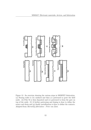
2. Patterning uses photolithography and etching to selectively expose layers for deposition, doping or etching according to the circuit design.
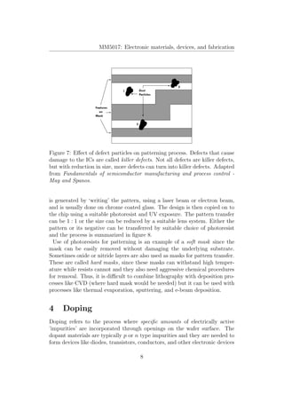
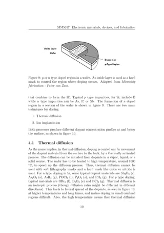
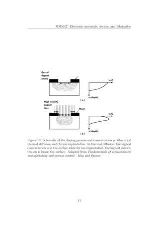
3. Doping introduces electrically active impurities through techniques like thermal diffusion or ion implantation to create semiconductor devices.