Download as PDF, PPTX

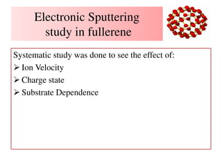
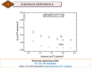


1. The document summarizes a study on the electronic sputtering of fullerene films under bombardment by energetic ions. 2. The study examined the effect of ion velocity, charge state, and substrate on the sputtering yield. It found that lower ion velocities and glass substrates resulted in higher sputtering yields. 3. The sputtering is attributed to a thermal spike mechanism where the excitation energy of bombarded electrons is coupled to the lattice, generating a rapid thermal spike that causes vaporization within a nanodimensional zone and material release from the surface.


![Thin_Film_Technology_introduction[1]](https://cdn.slidesharecdn.com/ss_thumbnails/1b4496c8-2102-411b-8465-a3dd3f398327-150205034538-conversion-gate02-thumbnail.jpg?width=640&height=640&fit=bounds)