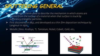
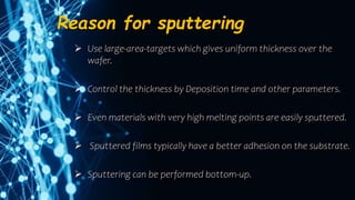
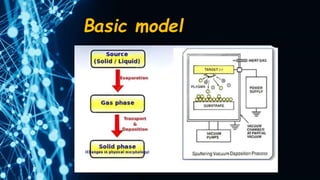
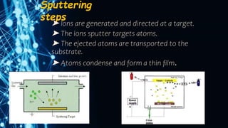
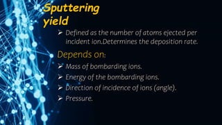
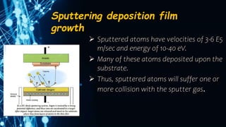
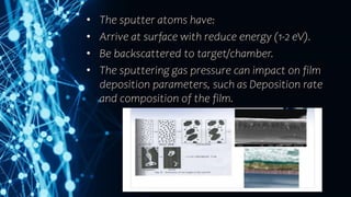
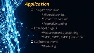
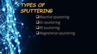
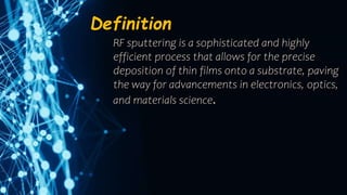
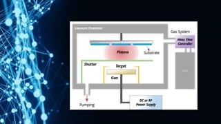
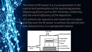
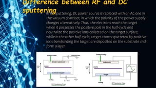
RF SPUTTERING
BY
S. Asma Saadhiya
N. Ayisha Balkish
B. Samyuktha
SPUTTERING GENERAL
 Sputtering is a term used to describe the mechanism in which atoms are
ejected from the surface of a material when that surface is stuck by
sufficiency energetic particles.
 First discovered in 1852, and developed as a thin film deposition technique by
Langmuir in 1920.
 Metallic films: Al-alloys, Ti, Tantalum, Nickel, Cobalt, Gold, etc.
Reason for sputtering
 Use large-area-targets which gives uniform thickness over the
wafer.
 Control the thickness by Deposition time and other parameters.
 Even materials with very high melting points are easily sputtered.
 Sputtered films typically have a better adhesion on the substrate.
 Sputtering can be performed bottom-up.
Basic model
Requirements
Vacuum
Inert gas
Power supply
Sputtering gas
Sputtering
steps
➤ lons are generated and directed at a target.
➤ The ions sputter targets atoms.
➤ The ejected atoms are transported to the
substrate.
➤ Atoms condense and form a thin film.
Sputtering
yield
 Defined as the number of atoms ejected per
incident ion.Determines the deposition rate.
Depends on:
 Mass of bombarding ions.
 Energy of the bombarding ions.
 Direction of incidence of ions (angle).
 Pressure.
Sputtering deposition film
growth
 Sputtered atoms have velocities of 3-6 E5
m/sec and energy of 10-40 eV.
 Many of these atoms deposited upon the
substrate.
 Thus, sputtered atoms will suffer one or
more collision with the sputter gas.
• The sputter atoms have:
• Arrive at surface with reduce energy (1-2 eV).
• Be backscattered to target/chamber.
• The sputtering gas pressure can impact on film
deposition parameters, such as Deposition rate
and composition of the film.
Application
 Thin film deposition:
*Microelectronics
*Decorative coating
*Protective coating
 Etching of targets:
*Microelectronics patterning
*CMOS, NMOS, PMOS fabrication
 Surface treatment:
*Hardening
TYPES OF
SPUTTERING
Reactive sputtering
Dc sputtering
Rf souttering
Magneteron sputtering
Reactive
sputtering
• Reactive gas is introduced into the sputtering chamber in
addition to the Argon plasma.
• The compound is formed by the elements of that gas
combining with the sputter material (Ex. TIN).
• The reaction is usually occurs either on the wafer surface
or on the target itself.
• As you add more reactive gas at some point the reaction
rate exceeds the sputtering rate.
• At this point the target surface switches from clean
metal to compound over a short time.
 The transition in target chemistry
changes sputtering conditions
dramatically !
Dc sputtering
E(e^ - )< 2eV - no ionization, elastic collisions only
E (e) > 2eV - inelastic collisions add energy to Ar
ionization (highest energy process, ~15eV)
Ar+e^ - A * r ^ 2 e^ -
Note: mass (e^ - )/mass (Ar) sim10^ -5
*energy transfer small
* e gain energy via elastic collisions until E>15eV
for ionization
* #ions ~ #neutrals sim 3 * 10 ^ 9 * c
*m ^ - 3 @ 10mT
• Light e- pulled towards walls faster than ions, leaving slightly
more ions in glow region
• Light e- move away from cathode faster than ions, leading
to a large field, high acceleration of ions into cathode
• high-E ions (10keV to 1 MeV) knock target material loose
resulting plume of neutrals
• new electrons from impact reactions replenish the plasma
Parameters for DC
Sputtering
● Sputter voltage
typically -2 to -5 kV
●Substrate Bias Voltage
substrate is being bombarded by electrons and ions
from target and plasma sputtering film while you deposit
neutral atoms deposit independently put negative bias on
the substrate to control this can significantly change film
properties
●Deposition rate
changes with Ar pressure
increases with sputter yield
• usually increases with high voltage
Definition
RF sputtering is a sophisticated and highly
efficient process that allows for the precise
deposition of thin films onto a substrate, paving
the way for advancements in electronics, optics,
and materials science.
Process of sputtering
• The RF sputtering process begins with the careful
selection of a solid target material.
• The material is decided based on the specific properties
desired for the ensuing thin film deposition.
• This choice often involves selecting from a range of
materials that include metals, semiconductors and
insulators.
• The subsequent steps take place within a vacuum
chamber.
• The vacuum chamber is an essential component of the
process designed to eliminate interference from the
surrounding atmosphere and establish a meticulously
controlled environment.
• Once the target material is chosen, the substrate,
onto which the thin film will be deposited, is placed
strategically within the vacuum chamber to ensure
precision in the subsequent deposition steps.
• To facilitate the sputtering process, an inert gas,
typically argon, is introduced into the vacuum
chamber.
• This inert gas serves as a medium through which
momentum is transferred from ionized gas particles
(plasma) to the selected target material.
• RF power is introduced in the chamber leading
to the creation of a plasma within the chamber.
• The high-frequency oscillations of the RF power
enhance the ionization of the gas, creating a
more energetic and controlled plasma
compared to DC sputtering.
• As the RF power energizes the plasma, high-energy
ions within the plasma collide with the atoms
constituting the target material.
• This collision process effectively dislodges atoms
from the surface of the target material.
• These dislodged atoms then travel through the
vacuum chamber, navigating the controlled
environment and ultimately settling onto the
strategically positioned substrate.
• This results in the formation of a thin film on the
substrate, transferring the desired properties of the
initially chosen target material to the substrate.
RF Power in RF Sputtering
• The amount of RF power required for RF sputtering can
vary depending on several factors, including the specific
materials being used, the size and geometry of the
sputtering system, the desired deposition rate, and the
characteristics of the thin film being deposited.
• Generally, RF sputtering systems operate in the radio
frequency range, typically between 13.56 MHz and 100
MHz
• As the RF power is applied to the target material,
it creates a plasma in the vacuum chamber.
• The power level influences the ionization of the
inert gas (commonly argon) and, consequently,
the sputtering rate.
• Higher RF power levels can lead to a more
energetic plasma, which may result in a higher
deposition rate and enhanced film properties.
• Typically, RF power levels for sputtering can
range from a few hundred watts to several
kilowatts.
• For smaller laboratory-scale systems, the power
might be in the range of 100-500 watts.
• In larger industrial-scale systems, the RF power
can be much higher, ranging from several
hundred watts to several kilowatts.
• The optimal power level for RF sputtering is often
determined experimentally for a specific set of
parameters, including the type of target material,
the substrate material, and the desired film
properties.
• Process engineers and researchers typically
perform power optimization studies to find the
most efficient and effective power level for a
given deposition process
• The choice of RF power is a crucial parameter in the
control and optimization of the sputtering process,
influencing factors such as film thickness, uniformity,
and the overall efficiency of the deposition.
• It's common for operators and researchers to adjust
and fine-tune the RF power to achieve the desired thin
film characteristics in a reproducible manner.
Advantages of RF Sputtering
 Uniform Thin Films: RF sputtering provides excellent control
over the deposition process, resulting in highly uniform and
reproducible thin films.
 Target Material Variety: RF sputtering supports a wide range
of target materials, including metals, alloys, and compound
materials, allowing for the deposition of diverse thin films with
specific properties.
 Reduced Heating: The use of RF power reduces the thermal
stress on the target material, enabling the deposition of thin
films on temperature-sensitive substrates.
 High Deposition Rates: RF sputtering can achieve higher
deposition rates compared to DC sputtering, making it suitable
for large-scale production.
Applications of RF
Sputtering:
 Semiconductor Manufacturing: RF sputtering is widely employed in the
production of semiconductor devices, including integrated circuits and thin-film
transistors.
 Optical Coatings: The precision and uniformity of RF-sputtered thin films make
them ideal for optical coatings, such as anti-reflective coatings on lenses and
mirrors.
 Solar Cells: RF sputtering is utilized in the manufacturing of thin-film solar cells,
contributing to the development of efficient and cost-effective solar energy
solutions.
 Data Storage: The technology is integral in the production of magnetic thin films
for use in hard disk drives and other data storage devices.
MAGNETRON
SPUTTERING
Here magnets are used to increase the percentage of
electrons that take part in ionization events, increase
probability of electrons striking Ar, increase electron path
length, so the ionization efficiency is increased significantly.
Another reasons to use magnets:
Lower voltage needed to strike plasma. Controls
uniformity.
Reduce wafer heating from electron bombardment.
Increased deposition rate
- Good control over reactive sputtering
Strong electric and magnetic
field
• Magnetron sputtering is a highly versatile thin
film deposition technique for coating films with
excellent adhesion and high density.
• A type of physical vapor deposition (PVD)
coating technology, magnetron sputtering is a
plasma-based coating process where a
magnetically confined plasma is created near
the surface of a target material, Positively
charged energetic ions from the plasma collide
with the negatively charged target material,
and atoms from the target are ejected or
"sputtered", which then deposit on a substrate.
PROCESS
The magnetron device has a dipole magnetic configuration to trap the
electrons emitted at the cathode. In this way the excitation and
ionization rates are enhanced, allowing the operation of the discharge
at low pressures, below 10 mbar. To create this dipole configuration,
usually three rows of permanent magnets are arranged in the following
order, N- S-N or S-N-5, that is, the inner row must have an opposite
polarization in relation to the outer rows. On the balanced
magnetrons, the magnets have the same strength. On the unbalanced
magnetron the inner magnet is weakened. In this way, more electrons
are lost to the plasma, resulting in an increase of the plasma length,
towards the substrate. In this way, the substrate current increases
dramatically, as well as the coating quality
Difference between RF and DC
sputtering
• In RF sputtering, DC power source is replaced with an AC one in
the vacuum chamber, in which the polarity of the power supply
changes alternatively. Thus, the electrons reach the target
when it possesses the positive pole in the half-cycle and
neutralize the positive ions collected on the target surface;
while in the other half-cycle, target atoms sputtered by positive
ions bombarding the target are deposited on the substrate and
form a layer
• To electrically discharge the target during sputtering a
frequency of 1MHz or higher is needed. Application of an
alternative current to an insulating target in this frequency
range is equivalent to current flow through dielectric media
of capacitors in series.Since the frequency normally used in
this method is in the range of 5-30 MHz, it is commonly
known as Radio Frequency (RF) Sputtering.
Why Frequency of 13.56 MHz is
Used?
• In order to prevent the interference between the
frequencies used in telecommunication services, the
standard radio frequency recommended by the ITU Radio
Regulations (2012) for operating industrial (I), scientific
(S), and medical (M) instruments, which is called ISM, is
centered at 13.56 MHz with a bandwidth of 14 kHz.Also
this frequency is low enough to provide sufficient time
for the momentum transfer of argon ions to the target.
At higher frequencies, Ar ions are practically immobilized
and electrons play effective role in the sputtering process
(more like e-beam evaporation method).
RF Sputtering Advantages over DC
Sputtering
• Now, we will examine DC vs RF sputtering and explain the
advantages of RF magnetron sputtering.The plasma formation is not
limited to the cathode or target surface and can extend in the
vacuum chamber.
• Higher plasma currents in lower working pressure: Plasma can be
maintained in less working gas pressure (1-15 mTorr), which results in
less collision between sputtered atoms and chamber molecules and
larger mean free path for target atoms. Also, the magnetic field of
the magnetron creates a boundary tunnel which traps the electrons
near target surface and increases sputtering yield in lower pressures.
• By eliminating charge build up on the cathode
surface, plasma arcing and layer quality control
issues will be eradicated, so more uniform layer
deposition is possible.
• In RF sputtering larger surface of the target is
involved in the sputtering process, resulting in
decreasing the so called ‘Race Track Erosion’ on
its surface, so the lifetime of the target is
enhanced.
Disadvantages of RF
Sputtering
• Compared to DC Sputtering, higher voltages
should be applied in order to increase the
sputtering rate, leading to more heating
effect on the substrate.
• This method is more complicated and
expensive compared to traditional DC
sputtering.
• RF current is transported on the skin or surface of the
conductors and not through them, so special connectors
and cables is needed for RF sputtering.
• With decrease in secondary electrons over cathode,
deposition rate is lower than DC method and higher power
level is needed to increase deposition rate
• .As a consequence of lower sputtering yields of electrically
insulating targets, resulting in lower deposition rates, RF
sources with higher powers should be employed, in
contrast to DC sputtering.
RF SPUTTERING.pptx engineering physics..

RF SPUTTERING.pptx engineering physics..

  • 1.
    RF SPUTTERING BY S. AsmaSaadhiya N. Ayisha Balkish B. Samyuktha
  • 2.
    SPUTTERING GENERAL  Sputteringis a term used to describe the mechanism in which atoms are ejected from the surface of a material when that surface is stuck by sufficiency energetic particles.  First discovered in 1852, and developed as a thin film deposition technique by Langmuir in 1920.  Metallic films: Al-alloys, Ti, Tantalum, Nickel, Cobalt, Gold, etc.
  • 3.
    Reason for sputtering Use large-area-targets which gives uniform thickness over the wafer.  Control the thickness by Deposition time and other parameters.  Even materials with very high melting points are easily sputtered.  Sputtered films typically have a better adhesion on the substrate.  Sputtering can be performed bottom-up.
  • 4.
  • 5.
  • 6.
    Sputtering steps ➤ lons aregenerated and directed at a target. ➤ The ions sputter targets atoms. ➤ The ejected atoms are transported to the substrate. ➤ Atoms condense and form a thin film.
  • 7.
    Sputtering yield  Defined asthe number of atoms ejected per incident ion.Determines the deposition rate. Depends on:  Mass of bombarding ions.  Energy of the bombarding ions.  Direction of incidence of ions (angle).  Pressure.
  • 8.
    Sputtering deposition film growth Sputtered atoms have velocities of 3-6 E5 m/sec and energy of 10-40 eV.  Many of these atoms deposited upon the substrate.  Thus, sputtered atoms will suffer one or more collision with the sputter gas.
  • 9.
    • The sputteratoms have: • Arrive at surface with reduce energy (1-2 eV). • Be backscattered to target/chamber. • The sputtering gas pressure can impact on film deposition parameters, such as Deposition rate and composition of the film.
  • 10.
    Application  Thin filmdeposition: *Microelectronics *Decorative coating *Protective coating  Etching of targets: *Microelectronics patterning *CMOS, NMOS, PMOS fabrication  Surface treatment: *Hardening
  • 11.
    TYPES OF SPUTTERING Reactive sputtering Dcsputtering Rf souttering Magneteron sputtering
  • 12.
    Reactive sputtering • Reactive gasis introduced into the sputtering chamber in addition to the Argon plasma. • The compound is formed by the elements of that gas combining with the sputter material (Ex. TIN). • The reaction is usually occurs either on the wafer surface or on the target itself. • As you add more reactive gas at some point the reaction rate exceeds the sputtering rate. • At this point the target surface switches from clean metal to compound over a short time.
  • 13.
     The transitionin target chemistry changes sputtering conditions dramatically !
  • 15.
    Dc sputtering E(e^ -)< 2eV - no ionization, elastic collisions only E (e) > 2eV - inelastic collisions add energy to Ar ionization (highest energy process, ~15eV) Ar+e^ - A * r ^ 2 e^ - Note: mass (e^ - )/mass (Ar) sim10^ -5 *energy transfer small * e gain energy via elastic collisions until E>15eV for ionization * #ions ~ #neutrals sim 3 * 10 ^ 9 * c *m ^ - 3 @ 10mT
  • 16.
    • Light e-pulled towards walls faster than ions, leaving slightly more ions in glow region • Light e- move away from cathode faster than ions, leading to a large field, high acceleration of ions into cathode • high-E ions (10keV to 1 MeV) knock target material loose resulting plume of neutrals • new electrons from impact reactions replenish the plasma
  • 17.
    Parameters for DC Sputtering ●Sputter voltage typically -2 to -5 kV ●Substrate Bias Voltage substrate is being bombarded by electrons and ions from target and plasma sputtering film while you deposit neutral atoms deposit independently put negative bias on the substrate to control this can significantly change film properties ●Deposition rate changes with Ar pressure increases with sputter yield • usually increases with high voltage
  • 18.
    Definition RF sputtering isa sophisticated and highly efficient process that allows for the precise deposition of thin films onto a substrate, paving the way for advancements in electronics, optics, and materials science.
  • 20.
    Process of sputtering •The RF sputtering process begins with the careful selection of a solid target material. • The material is decided based on the specific properties desired for the ensuing thin film deposition. • This choice often involves selecting from a range of materials that include metals, semiconductors and insulators. • The subsequent steps take place within a vacuum chamber. • The vacuum chamber is an essential component of the process designed to eliminate interference from the surrounding atmosphere and establish a meticulously controlled environment.
  • 21.
    • Once thetarget material is chosen, the substrate, onto which the thin film will be deposited, is placed strategically within the vacuum chamber to ensure precision in the subsequent deposition steps. • To facilitate the sputtering process, an inert gas, typically argon, is introduced into the vacuum chamber. • This inert gas serves as a medium through which momentum is transferred from ionized gas particles (plasma) to the selected target material.
  • 22.
    • RF poweris introduced in the chamber leading to the creation of a plasma within the chamber. • The high-frequency oscillations of the RF power enhance the ionization of the gas, creating a more energetic and controlled plasma compared to DC sputtering.
  • 23.
    • As theRF power energizes the plasma, high-energy ions within the plasma collide with the atoms constituting the target material. • This collision process effectively dislodges atoms from the surface of the target material. • These dislodged atoms then travel through the vacuum chamber, navigating the controlled environment and ultimately settling onto the strategically positioned substrate. • This results in the formation of a thin film on the substrate, transferring the desired properties of the initially chosen target material to the substrate.
  • 24.
    RF Power inRF Sputtering • The amount of RF power required for RF sputtering can vary depending on several factors, including the specific materials being used, the size and geometry of the sputtering system, the desired deposition rate, and the characteristics of the thin film being deposited. • Generally, RF sputtering systems operate in the radio frequency range, typically between 13.56 MHz and 100 MHz
  • 25.
    • As theRF power is applied to the target material, it creates a plasma in the vacuum chamber. • The power level influences the ionization of the inert gas (commonly argon) and, consequently, the sputtering rate. • Higher RF power levels can lead to a more energetic plasma, which may result in a higher deposition rate and enhanced film properties.
  • 26.
    • Typically, RFpower levels for sputtering can range from a few hundred watts to several kilowatts. • For smaller laboratory-scale systems, the power might be in the range of 100-500 watts. • In larger industrial-scale systems, the RF power can be much higher, ranging from several hundred watts to several kilowatts.
  • 27.
    • The optimalpower level for RF sputtering is often determined experimentally for a specific set of parameters, including the type of target material, the substrate material, and the desired film properties. • Process engineers and researchers typically perform power optimization studies to find the most efficient and effective power level for a given deposition process
  • 28.
    • The choiceof RF power is a crucial parameter in the control and optimization of the sputtering process, influencing factors such as film thickness, uniformity, and the overall efficiency of the deposition. • It's common for operators and researchers to adjust and fine-tune the RF power to achieve the desired thin film characteristics in a reproducible manner.
  • 29.
    Advantages of RFSputtering  Uniform Thin Films: RF sputtering provides excellent control over the deposition process, resulting in highly uniform and reproducible thin films.  Target Material Variety: RF sputtering supports a wide range of target materials, including metals, alloys, and compound materials, allowing for the deposition of diverse thin films with specific properties.  Reduced Heating: The use of RF power reduces the thermal stress on the target material, enabling the deposition of thin films on temperature-sensitive substrates.  High Deposition Rates: RF sputtering can achieve higher deposition rates compared to DC sputtering, making it suitable for large-scale production.
  • 30.
    Applications of RF Sputtering: Semiconductor Manufacturing: RF sputtering is widely employed in the production of semiconductor devices, including integrated circuits and thin-film transistors.  Optical Coatings: The precision and uniformity of RF-sputtered thin films make them ideal for optical coatings, such as anti-reflective coatings on lenses and mirrors.  Solar Cells: RF sputtering is utilized in the manufacturing of thin-film solar cells, contributing to the development of efficient and cost-effective solar energy solutions.  Data Storage: The technology is integral in the production of magnetic thin films for use in hard disk drives and other data storage devices.
  • 31.
    MAGNETRON SPUTTERING Here magnets areused to increase the percentage of electrons that take part in ionization events, increase probability of electrons striking Ar, increase electron path length, so the ionization efficiency is increased significantly. Another reasons to use magnets: Lower voltage needed to strike plasma. Controls uniformity. Reduce wafer heating from electron bombardment. Increased deposition rate - Good control over reactive sputtering
  • 32.
    Strong electric andmagnetic field • Magnetron sputtering is a highly versatile thin film deposition technique for coating films with excellent adhesion and high density. • A type of physical vapor deposition (PVD) coating technology, magnetron sputtering is a plasma-based coating process where a magnetically confined plasma is created near the surface of a target material, Positively charged energetic ions from the plasma collide with the negatively charged target material, and atoms from the target are ejected or "sputtered", which then deposit on a substrate.
  • 33.
    PROCESS The magnetron devicehas a dipole magnetic configuration to trap the electrons emitted at the cathode. In this way the excitation and ionization rates are enhanced, allowing the operation of the discharge at low pressures, below 10 mbar. To create this dipole configuration, usually three rows of permanent magnets are arranged in the following order, N- S-N or S-N-5, that is, the inner row must have an opposite polarization in relation to the outer rows. On the balanced magnetrons, the magnets have the same strength. On the unbalanced magnetron the inner magnet is weakened. In this way, more electrons are lost to the plasma, resulting in an increase of the plasma length, towards the substrate. In this way, the substrate current increases dramatically, as well as the coating quality
  • 35.
    Difference between RFand DC sputtering • In RF sputtering, DC power source is replaced with an AC one in the vacuum chamber, in which the polarity of the power supply changes alternatively. Thus, the electrons reach the target when it possesses the positive pole in the half-cycle and neutralize the positive ions collected on the target surface; while in the other half-cycle, target atoms sputtered by positive ions bombarding the target are deposited on the substrate and form a layer
  • 36.
    • To electricallydischarge the target during sputtering a frequency of 1MHz or higher is needed. Application of an alternative current to an insulating target in this frequency range is equivalent to current flow through dielectric media of capacitors in series.Since the frequency normally used in this method is in the range of 5-30 MHz, it is commonly known as Radio Frequency (RF) Sputtering.
  • 37.
    Why Frequency of13.56 MHz is Used? • In order to prevent the interference between the frequencies used in telecommunication services, the standard radio frequency recommended by the ITU Radio Regulations (2012) for operating industrial (I), scientific (S), and medical (M) instruments, which is called ISM, is centered at 13.56 MHz with a bandwidth of 14 kHz.Also this frequency is low enough to provide sufficient time for the momentum transfer of argon ions to the target. At higher frequencies, Ar ions are practically immobilized and electrons play effective role in the sputtering process (more like e-beam evaporation method).
  • 38.
    RF Sputtering Advantagesover DC Sputtering • Now, we will examine DC vs RF sputtering and explain the advantages of RF magnetron sputtering.The plasma formation is not limited to the cathode or target surface and can extend in the vacuum chamber. • Higher plasma currents in lower working pressure: Plasma can be maintained in less working gas pressure (1-15 mTorr), which results in less collision between sputtered atoms and chamber molecules and larger mean free path for target atoms. Also, the magnetic field of the magnetron creates a boundary tunnel which traps the electrons near target surface and increases sputtering yield in lower pressures.
  • 39.
    • By eliminatingcharge build up on the cathode surface, plasma arcing and layer quality control issues will be eradicated, so more uniform layer deposition is possible. • In RF sputtering larger surface of the target is involved in the sputtering process, resulting in decreasing the so called ‘Race Track Erosion’ on its surface, so the lifetime of the target is enhanced.
  • 40.
    Disadvantages of RF Sputtering •Compared to DC Sputtering, higher voltages should be applied in order to increase the sputtering rate, leading to more heating effect on the substrate. • This method is more complicated and expensive compared to traditional DC sputtering.
  • 41.
    • RF currentis transported on the skin or surface of the conductors and not through them, so special connectors and cables is needed for RF sputtering. • With decrease in secondary electrons over cathode, deposition rate is lower than DC method and higher power level is needed to increase deposition rate • .As a consequence of lower sputtering yields of electrically insulating targets, resulting in lower deposition rates, RF sources with higher powers should be employed, in contrast to DC sputtering.