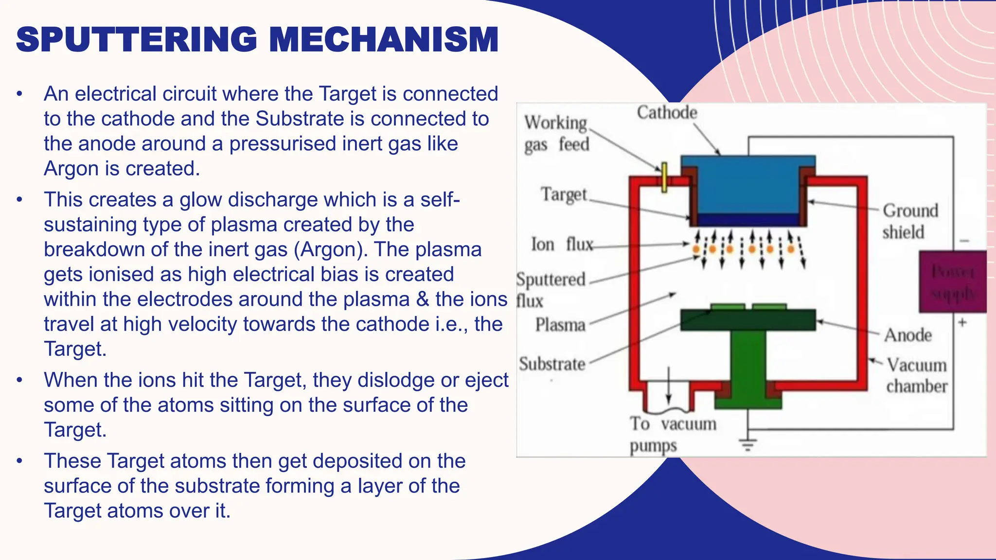
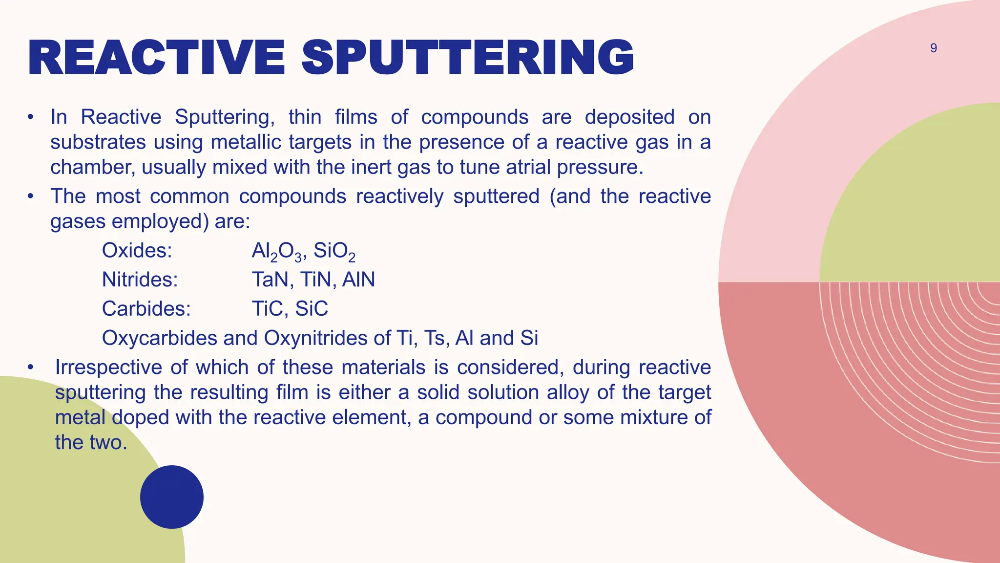
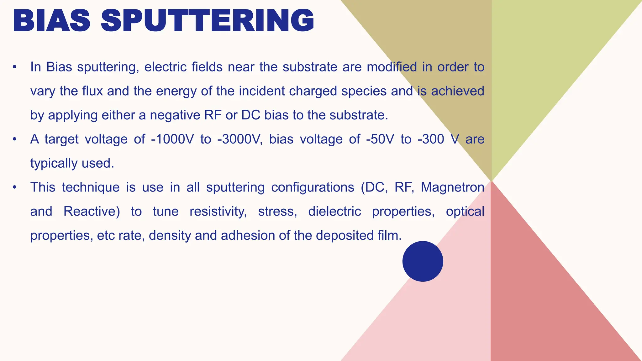
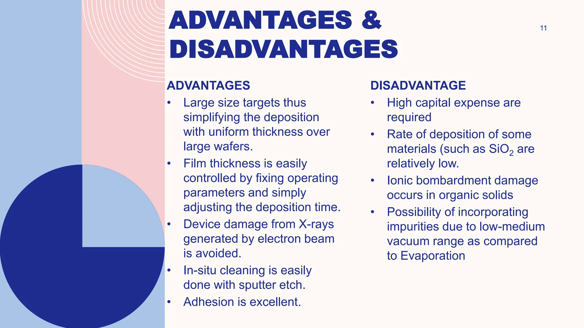
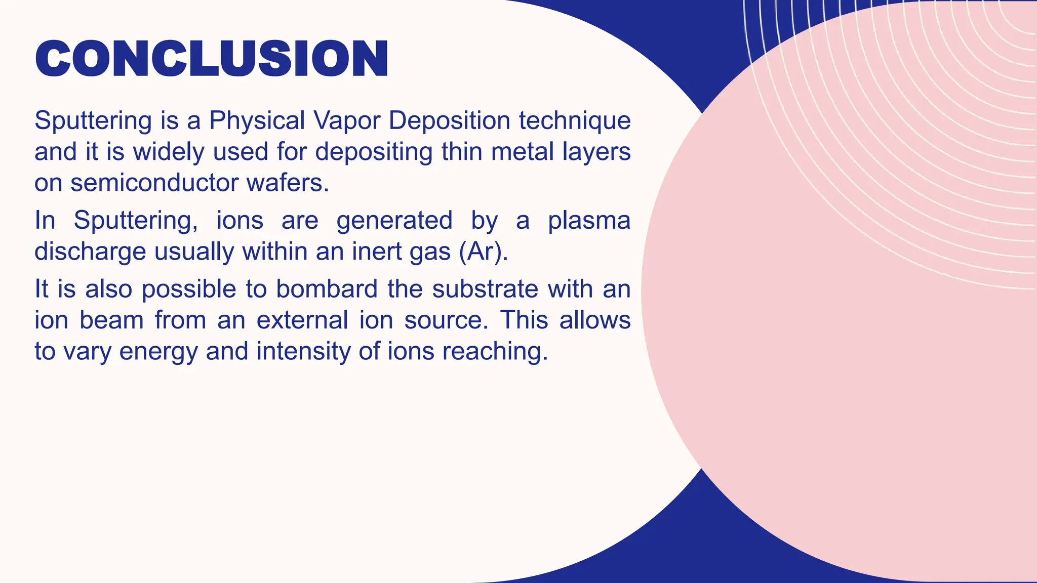
SlideShare a Scribd company logo
SPUTTERING
Lalrinfeli Ralte
ECE/20/08
CONTENTS
• Introduction
• Sputtering Mechanism
• Sputter Yield
• Different Techniques of Sputtering
DC Sputtering
RF Sputtering
Magnetron Sputtering
Reactive Sputtering
Bias Sputtering
• Advantages and Disadvantages
• Conclusion
INTRODUCTION 3
Sputtering is a mechanism by which atoms are dislodged
from the surface of a material as a result of collision with high
energy particles.
It is a type of Physical Vapor Deposition (PVD).
It can be described as a sequence of these steps:
1) Ions are generated and directed at target material.
2) The ions sputter atoms from the target
3) Sputtered atoms get transported to the substrate through a
region of reduced pressure
4) The sputtered atoms get condensed on the substrate,
forming a thin film.
SPUTTERING MECHANISM
• An electrical circuit where the Target is connected
to the cathode and the Substrate is connected to
the anode around a pressurised inert gas like
Argon is created.
• This creates a glow discharge which is a self-
sustaining type of plasma created by the
breakdown of the inert gas (Argon). The plasma
gets ionised as high electrical bias is created
within the electrodes around the plasma & the ions
travel at high velocity towards the cathode i.e., the
Target.
• When the ions hit the Target, they dislodge or eject
some of the atoms sitting on the surface of the
Target.
• These Target atoms then get deposited on the
surface of the substrate forming a layer of the
Target atoms over it.
SPUTTER YIELD 5
Sputter yield is the ratio of number of sputtered atoms to
number of incident ions.
𝑆 =
𝑛𝑢𝑚𝑏𝑒𝑟 𝑜𝑓 𝑠𝑝𝑢𝑡𝑡𝑒𝑟𝑒𝑑 𝑎𝑡𝑜𝑚𝑠
𝑛𝑢𝑚𝑏𝑒𝑟 𝑜𝑓 𝑖𝑛𝑐𝑖𝑑𝑒𝑛𝑡 𝑎𝑡𝑜𝑚𝑠
Sputter Yield depends on :
• 𝑆 ∝
1
𝑏𝑖𝑛𝑑𝑖𝑛𝑔 𝑒𝑛𝑒𝑟𝑔𝑦
• 𝑆 ∝ 𝐸𝑛𝑒𝑟𝑔𝑦 𝑜𝑓 𝑖𝑜𝑛𝑠
• 𝑆 ∝ 𝐼𝑛𝑐𝑖𝑑𝑒𝑛𝑡 𝑎𝑛𝑔𝑙𝑒 𝑜𝑓 𝑖𝑜𝑛𝑠
• Reduction in deposition of pressure gives better yield.
DC SPUTTERING
6
 Here a D.C electric field is impressed across the
electrodes which are located in the inert gas.
 The deposition rate depends on the pressure of the inert
gas and the DC voltage.
 As pressure is increased at fixed voltage, the mean free
path is decreased & more ions are generated. If pressure
is too high, the sputtered atoms undergo increased
collisional scattering and are not efficiently deposited.
 Energy is gained via elastic collisions until E > 15 eV for
ionisation.
 𝐴𝑟 + 𝑒− → 𝐴𝑟+ + 2𝑒−
The Optimum condition is shown in the shaded region of the
graph.
This range of pressure is suitable for DC Sputtering.
RF SPUTTERING
• The RF Sputtering helps to deposit insulating thin
films (resistivity > 106 Ω-cm).
• It is usually carried out with 1 to 3 kV peak-to-peak
RF potential.
• At AC signal above 50 kHz, electrons oscillating in
the glow region acquire enough energy to cause
ionising collisions, reducing the need for 2°
electrons to sustain the discharge.
• Also, RF voltages can be coupled through any kind
of impedance so that the electrodes need not be
conductors. So it is possible to sputter any material
irrespective of its resistivity.
• Typical RF frequencies employed is 13.56 MHz.
MAGNETRON SPUTTERING
8
• This technology uses powerful magnets to confine the
"glow discharge" plasma to the region closest to the target
plate.
• That vastly improves the deposition rate by maintaining a
higher density of ions, which makes the electron/gas
molecule collision process much more efficient.
• Uses either DC or RF power.
• A magnetic field of 100-200 gauss is used, resulting in
field lines which confine electrons to the region embraced
by them
• The discharge region is in the shape of a torroid or
elongated ring, with extensive sputtering of the target in
these regions.
• Substrates are usually placed on a rotating anode in order
to obtain uniform film deposition.
REACTIVE SPUTTERING 9
• In Reactive Sputtering, thin films of compounds are deposited on
substrates using metallic targets in the presence of a reactive gas in a
chamber, usually mixed with the inert gas to tune atrial pressure.
• The most common compounds reactively sputtered (and the reactive
gases employed) are:
Oxides: Al2O3, SiO2
Nitrides: TaN, TiN, AlN
Carbides: TiC, SiC
Oxycarbides and Oxynitrides of Ti, Ts, Al and Si
• Irrespective of which of these materials is considered, during reactive
sputtering the resulting film is either a solid solution alloy of the target
metal doped with the reactive element, a compound or some mixture of
the two.
BIAS SPUTTERING
• In Bias sputtering, electric fields near the substrate are modified in order to
vary the flux and the energy of the incident charged species and is achieved
by applying either a negative RF or DC bias to the substrate.
• A target voltage of -1000V to -3000V, bias voltage of -50V to -300 V are
typically used.
• This technique is use in all sputtering configurations (DC, RF, Magnetron
and Reactive) to tune resistivity, stress, dielectric properties, optical
properties, etc rate, density and adhesion of the deposited film.
ADVANTAGES &
DISADVANTAGES
11
ADVANTAGES
• Large size targets thus
simplifying the deposition
with uniform thickness over
large wafers.
• Film thickness is easily
controlled by fixing operating
parameters and simply
adjusting the deposition time.
• Device damage from X-rays
generated by electron beam
is avoided.
• In-situ cleaning is easily
done with sputter etch.
• Adhesion is excellent.
DISADVANTAGE
• High capital expense are
required
• Rate of deposition of some
materials (such as SiO2 are
relatively low.
• Ionic bombardment damage
occurs in organic solids
• Possibility of incorporating
impurities due to low-medium
vacuum range as compared
to Evaporation
CONCLUSION
Sputtering is a Physical Vapor Deposition technique
and it is widely used for depositing thin metal layers
on semiconductor wafers.
In Sputtering, ions are generated by a plasma
discharge usually within an inert gas (Ar).
It is also possible to bombard the substrate with an
ion beam from an external ion source. This allows
to vary energy and intensity of ions reaching.
THANK YOU

More Related Content

What's hot

dip coating
dip coatingdip coating
dip coating
engrktk
 
Apps of thin films
Apps of thin filmsApps of thin films
Apps of thin films
Aneetta Davis
 
Pulsed laser deposition
Pulsed laser depositionPulsed laser deposition
Pulsed laser deposition
Oleg Maksimov
 
Chemical vapor deposition (cvd)
Chemical vapor deposition (cvd)Chemical vapor deposition (cvd)
Chemical vapor deposition (cvd)
Khalid Raza
 
Epitaxy growth
Epitaxy growthEpitaxy growth
Epitaxy growth
Rutuja Solkar
 
Physical Vapour Deposition (PVD)
Physical Vapour Deposition (PVD)Physical Vapour Deposition (PVD)
Physical Vapour Deposition (PVD)
jitendrahemwani
 
Thin films
Thin films Thin films
Thin films
srirangan mahesh
 
Sputtering process and its types
Sputtering process and its typesSputtering process and its types
Sputtering process and its types
MuhammadWajid37
 
why and how thin films
why and how thin filmswhy and how thin films
why and how thin films
sumit__kumar
 
Thin films
Thin filmsThin films
Thin films
Nischith Nbs
 
Preparation of thin films
Preparation of thin filmsPreparation of thin films
Preparation of thin films
Gandhimathi Muthuselvam
 
Pulse laser depostion of thin film
Pulse laser depostion of thin filmPulse laser depostion of thin film
Pulse laser depostion of thin film
Abdalla Darwish
 
Oxidation--ABU SYED KUET
Oxidation--ABU SYED KUETOxidation--ABU SYED KUET
Oxidation--ABU SYED KUET
A. S. M. Jannatul Islam
 
Thin-film Production
Thin-film ProductionThin-film Production
Thin-film Production
Shekh Saadi Biplob
 
Float Zone, Bridgman Techniques--ABU SYED KUET
Float Zone, Bridgman Techniques--ABU SYED KUETFloat Zone, Bridgman Techniques--ABU SYED KUET
Float Zone, Bridgman Techniques--ABU SYED KUET
A. S. M. Jannatul Islam
 
Size effect of nanomaterials part1
Size effect of nanomaterials part1Size effect of nanomaterials part1
Size effect of nanomaterials part1
Mugilan Narayanasamy
 
laser ablation and pyrolysis for micro machining and nano fabrication
laser ablation and pyrolysis for micro machining and nano fabricationlaser ablation and pyrolysis for micro machining and nano fabrication
laser ablation and pyrolysis for micro machining and nano fabrication
JAISMON FRANCIS
 
Chemical Vapour Deposition
Chemical Vapour DepositionChemical Vapour Deposition
Chemical Vapour Deposition
aroosa khan
 
Chemical vapor deposition and its types 120589
Chemical vapor deposition and its types 120589Chemical vapor deposition and its types 120589
Chemical vapor deposition and its types 120589
Adnan Majeed
 
Rani
RaniRani

What's hot (20)

dip coating
dip coatingdip coating
dip coating
 
Apps of thin films
Apps of thin filmsApps of thin films
Apps of thin films
 
Pulsed laser deposition
Pulsed laser depositionPulsed laser deposition
Pulsed laser deposition
 
Chemical vapor deposition (cvd)
Chemical vapor deposition (cvd)Chemical vapor deposition (cvd)
Chemical vapor deposition (cvd)
 
Epitaxy growth
Epitaxy growthEpitaxy growth
Epitaxy growth
 
Physical Vapour Deposition (PVD)
Physical Vapour Deposition (PVD)Physical Vapour Deposition (PVD)
Physical Vapour Deposition (PVD)
 
Thin films
Thin films Thin films
Thin films
 
Sputtering process and its types
Sputtering process and its typesSputtering process and its types
Sputtering process and its types
 
why and how thin films
why and how thin filmswhy and how thin films
why and how thin films
 
Thin films
Thin filmsThin films
Thin films
 
Preparation of thin films
Preparation of thin filmsPreparation of thin films
Preparation of thin films
 
Pulse laser depostion of thin film
Pulse laser depostion of thin filmPulse laser depostion of thin film
Pulse laser depostion of thin film
 
Oxidation--ABU SYED KUET
Oxidation--ABU SYED KUETOxidation--ABU SYED KUET
Oxidation--ABU SYED KUET
 
Thin-film Production
Thin-film ProductionThin-film Production
Thin-film Production
 
Float Zone, Bridgman Techniques--ABU SYED KUET
Float Zone, Bridgman Techniques--ABU SYED KUETFloat Zone, Bridgman Techniques--ABU SYED KUET
Float Zone, Bridgman Techniques--ABU SYED KUET
 
Size effect of nanomaterials part1
Size effect of nanomaterials part1Size effect of nanomaterials part1
Size effect of nanomaterials part1
 
laser ablation and pyrolysis for micro machining and nano fabrication
laser ablation and pyrolysis for micro machining and nano fabricationlaser ablation and pyrolysis for micro machining and nano fabrication
laser ablation and pyrolysis for micro machining and nano fabrication
 
Chemical Vapour Deposition
Chemical Vapour DepositionChemical Vapour Deposition
Chemical Vapour Deposition
 
Chemical vapor deposition and its types 120589
Chemical vapor deposition and its types 120589Chemical vapor deposition and its types 120589
Chemical vapor deposition and its types 120589
 
Rani
RaniRani
Rani
 

Similar to Sputtering ( Microelectronics & IC Technology )

Electron beam lithography
Electron beam lithographyElectron beam lithography
Electron beam lithography
karoline Enoch
 
Advanced Manufacturing Choices
Advanced Manufacturing ChoicesAdvanced Manufacturing Choices
Advanced Manufacturing Choices
Prasanth Kumar RAGUPATHY
 
MOSFET(ABOUT,FABRICATION)
MOSFET(ABOUT,FABRICATION)MOSFET(ABOUT,FABRICATION)
MOSFET(ABOUT,FABRICATION)
HARSHIT SONI
 
ION IMPLANTATION
ION IMPLANTATIONION IMPLANTATION
ION IMPLANTATION
AJAL A J
 
Optical Sources_SS-converted.pptx
Optical Sources_SS-converted.pptxOptical Sources_SS-converted.pptx
Optical Sources_SS-converted.pptx
THOMASTENCY1
 
Dr. jaishree nmr instrumentation
Dr. jaishree nmr instrumentationDr. jaishree nmr instrumentation
Dr. jaishree nmr instrumentation
Jaishree Bardapure
 
Passive device fabrication in Integrated circuits
Passive device fabrication in Integrated circuitsPassive device fabrication in Integrated circuits
Passive device fabrication in Integrated circuits
Abhishek Kadam
 
Prnciples of ionisation detection-Kiran
Prnciples of ionisation detection-KiranPrnciples of ionisation detection-Kiran
Prnciples of ionisation detection-Kiran
Kiran Ramakrishna
 
Study of Xray machines and functions.pdf
Study of Xray machines and functions.pdfStudy of Xray machines and functions.pdf
Study of Xray machines and functions.pdf
gametheory686sharech
 
Matching concept in Microelectronics
Matching concept in MicroelectronicsMatching concept in Microelectronics
Matching concept in Microelectronics
Tallinn University of Technology
 
ect 292 nano electronics
ect 292 nano electronics ect 292 nano electronics
ect 292 nano electronics
RenjithThomas13
 
ect 292 nano electronics
ect 292 nano electronics ect 292 nano electronics
ect 292 nano electronics
RenjithThomas13
 
Insulation and Dielectric Breakdown Design Paper SM54
Insulation and Dielectric Breakdown Design Paper SM54Insulation and Dielectric Breakdown Design Paper SM54
Insulation and Dielectric Breakdown Design Paper SM54
Subhash Mahla
 
SHIELDING & BONDING PPT.ppt
SHIELDING & BONDING PPT.pptSHIELDING & BONDING PPT.ppt
SHIELDING & BONDING PPT.ppt
hodeeeeee1
 
solar cell characteristics
solar cell characteristicssolar cell characteristics
solar cell characteristics
paneliya sagar
 
Unit 1 ppt notes /BM8702 /RADIOLOGICAL EQUIPMENTS
Unit 1 ppt notes /BM8702 /RADIOLOGICAL EQUIPMENTSUnit 1 ppt notes /BM8702 /RADIOLOGICAL EQUIPMENTS
Unit 1 ppt notes /BM8702 /RADIOLOGICAL EQUIPMENTS
KPR INSTITUE OF ENGINEERING AND TECHNOLOGY
 
Applications of Nanomaterials.pdf
Applications of Nanomaterials.pdfApplications of Nanomaterials.pdf
Applications of Nanomaterials.pdf
FikaduTakele1
 
laser Presentation.pptx
laser  Presentation.pptxlaser  Presentation.pptx
laser Presentation.pptx
Gaurang Joshi
 
Resistors
ResistorsResistors
Resistors
LorenzAlfuente
 
LASER ENGEENERING 2 .pdf
LASER ENGEENERING 2 .pdfLASER ENGEENERING 2 .pdf
LASER ENGEENERING 2 .pdf
THE CREATORS ACADEMY
 

Similar to Sputtering ( Microelectronics & IC Technology ) (20)

Electron beam lithography
Electron beam lithographyElectron beam lithography
Electron beam lithography
 
Advanced Manufacturing Choices
Advanced Manufacturing ChoicesAdvanced Manufacturing Choices
Advanced Manufacturing Choices
 
MOSFET(ABOUT,FABRICATION)
MOSFET(ABOUT,FABRICATION)MOSFET(ABOUT,FABRICATION)
MOSFET(ABOUT,FABRICATION)
 
ION IMPLANTATION
ION IMPLANTATIONION IMPLANTATION
ION IMPLANTATION
 
Optical Sources_SS-converted.pptx
Optical Sources_SS-converted.pptxOptical Sources_SS-converted.pptx
Optical Sources_SS-converted.pptx
 
Dr. jaishree nmr instrumentation
Dr. jaishree nmr instrumentationDr. jaishree nmr instrumentation
Dr. jaishree nmr instrumentation
 
Passive device fabrication in Integrated circuits
Passive device fabrication in Integrated circuitsPassive device fabrication in Integrated circuits
Passive device fabrication in Integrated circuits
 
Prnciples of ionisation detection-Kiran
Prnciples of ionisation detection-KiranPrnciples of ionisation detection-Kiran
Prnciples of ionisation detection-Kiran
 
Study of Xray machines and functions.pdf
Study of Xray machines and functions.pdfStudy of Xray machines and functions.pdf
Study of Xray machines and functions.pdf
 
Matching concept in Microelectronics
Matching concept in MicroelectronicsMatching concept in Microelectronics
Matching concept in Microelectronics
 
ect 292 nano electronics
ect 292 nano electronics ect 292 nano electronics
ect 292 nano electronics
 
ect 292 nano electronics
ect 292 nano electronics ect 292 nano electronics
ect 292 nano electronics
 
Insulation and Dielectric Breakdown Design Paper SM54
Insulation and Dielectric Breakdown Design Paper SM54Insulation and Dielectric Breakdown Design Paper SM54
Insulation and Dielectric Breakdown Design Paper SM54
 
SHIELDING & BONDING PPT.ppt
SHIELDING & BONDING PPT.pptSHIELDING & BONDING PPT.ppt
SHIELDING & BONDING PPT.ppt
 
solar cell characteristics
solar cell characteristicssolar cell characteristics
solar cell characteristics
 
Unit 1 ppt notes /BM8702 /RADIOLOGICAL EQUIPMENTS
Unit 1 ppt notes /BM8702 /RADIOLOGICAL EQUIPMENTSUnit 1 ppt notes /BM8702 /RADIOLOGICAL EQUIPMENTS
Unit 1 ppt notes /BM8702 /RADIOLOGICAL EQUIPMENTS
 
Applications of Nanomaterials.pdf
Applications of Nanomaterials.pdfApplications of Nanomaterials.pdf
Applications of Nanomaterials.pdf
 
laser Presentation.pptx
laser  Presentation.pptxlaser  Presentation.pptx
laser Presentation.pptx
 
Resistors
ResistorsResistors
Resistors
 
LASER ENGEENERING 2 .pdf
LASER ENGEENERING 2 .pdfLASER ENGEENERING 2 .pdf
LASER ENGEENERING 2 .pdf
 

Recently uploaded

学校原版美国波士顿大学毕业证学历学位证书原版一模一样
学校原版美国波士顿大学毕业证学历学位证书原版一模一样学校原版美国波士顿大学毕业证学历学位证书原版一模一样
学校原版美国波士顿大学毕业证学历学位证书原版一模一样
171ticu
 
CEC 352 - SATELLITE COMMUNICATION UNIT 1
CEC 352 - SATELLITE COMMUNICATION UNIT 1CEC 352 - SATELLITE COMMUNICATION UNIT 1
CEC 352 - SATELLITE COMMUNICATION UNIT 1
PKavitha10
 
Software Engineering and Project Management - Introduction, Modeling Concepts...
Software Engineering and Project Management - Introduction, Modeling Concepts...Software Engineering and Project Management - Introduction, Modeling Concepts...
Software Engineering and Project Management - Introduction, Modeling Concepts...
Prakhyath Rai
 
TIME TABLE MANAGEMENT SYSTEM testing.pptx
TIME TABLE MANAGEMENT SYSTEM testing.pptxTIME TABLE MANAGEMENT SYSTEM testing.pptx
TIME TABLE MANAGEMENT SYSTEM testing.pptx
CVCSOfficial
 
Properties Railway Sleepers and Test.pptx
Properties Railway Sleepers and Test.pptxProperties Railway Sleepers and Test.pptx
Properties Railway Sleepers and Test.pptx
MDSABBIROJJAMANPAYEL
 
CompEx~Manual~1210 (2).pdf COMPEX GAS AND VAPOURS
CompEx~Manual~1210 (2).pdf COMPEX GAS AND VAPOURSCompEx~Manual~1210 (2).pdf COMPEX GAS AND VAPOURS
CompEx~Manual~1210 (2).pdf COMPEX GAS AND VAPOURS
RamonNovais6
 
Mechanical Engineering on AAI Summer Training Report-003.pdf
Mechanical Engineering on AAI Summer Training Report-003.pdfMechanical Engineering on AAI Summer Training Report-003.pdf
Mechanical Engineering on AAI Summer Training Report-003.pdf
21UME003TUSHARDEB
 
AI + Data Community Tour - Build the Next Generation of Apps with the Einstei...
AI + Data Community Tour - Build the Next Generation of Apps with the Einstei...AI + Data Community Tour - Build the Next Generation of Apps with the Einstei...
AI + Data Community Tour - Build the Next Generation of Apps with the Einstei...
Paris Salesforce Developer Group
 
一比一原版(CalArts毕业证)加利福尼亚艺术学院毕业证如何办理
一比一原版(CalArts毕业证)加利福尼亚艺术学院毕业证如何办理一比一原版(CalArts毕业证)加利福尼亚艺术学院毕业证如何办理
一比一原版(CalArts毕业证)加利福尼亚艺术学院毕业证如何办理
ecqow
 
AI for Legal Research with applications, tools
AI for Legal Research with applications, toolsAI for Legal Research with applications, tools
AI for Legal Research with applications, tools
mahaffeycheryld
 
Curve Fitting in Numerical Methods Regression
Curve Fitting in Numerical Methods RegressionCurve Fitting in Numerical Methods Regression
Curve Fitting in Numerical Methods Regression
Nada Hikmah
 
Redefining brain tumor segmentation: a cutting-edge convolutional neural netw...
Redefining brain tumor segmentation: a cutting-edge convolutional neural netw...Redefining brain tumor segmentation: a cutting-edge convolutional neural netw...
Redefining brain tumor segmentation: a cutting-edge convolutional neural netw...
IJECEIAES
 
VARIABLE FREQUENCY DRIVE. VFDs are widely used in industrial applications for...
VARIABLE FREQUENCY DRIVE. VFDs are widely used in industrial applications for...VARIABLE FREQUENCY DRIVE. VFDs are widely used in industrial applications for...
VARIABLE FREQUENCY DRIVE. VFDs are widely used in industrial applications for...
PIMR BHOPAL
 
4. Mosca vol I -Fisica-Tipler-5ta-Edicion-Vol-1.pdf
4. Mosca vol I -Fisica-Tipler-5ta-Edicion-Vol-1.pdf4. Mosca vol I -Fisica-Tipler-5ta-Edicion-Vol-1.pdf
4. Mosca vol I -Fisica-Tipler-5ta-Edicion-Vol-1.pdf
Gino153088
 
Advanced control scheme of doubly fed induction generator for wind turbine us...
Advanced control scheme of doubly fed induction generator for wind turbine us...Advanced control scheme of doubly fed induction generator for wind turbine us...
Advanced control scheme of doubly fed induction generator for wind turbine us...
IJECEIAES
 
Gas agency management system project report.pdf
Gas agency management system project report.pdfGas agency management system project report.pdf
Gas agency management system project report.pdf
Kamal Acharya
 
Computational Engineering IITH Presentation
Computational Engineering IITH PresentationComputational Engineering IITH Presentation
Computational Engineering IITH Presentation
co23btech11018
 
Electric vehicle and photovoltaic advanced roles in enhancing the financial p...
Electric vehicle and photovoltaic advanced roles in enhancing the financial p...Electric vehicle and photovoltaic advanced roles in enhancing the financial p...
Electric vehicle and photovoltaic advanced roles in enhancing the financial p...
IJECEIAES
 
1FIDIC-CONSTRUCTION-CONTRACT-2ND-ED-2017-RED-BOOK.pdf
1FIDIC-CONSTRUCTION-CONTRACT-2ND-ED-2017-RED-BOOK.pdf1FIDIC-CONSTRUCTION-CONTRACT-2ND-ED-2017-RED-BOOK.pdf
1FIDIC-CONSTRUCTION-CONTRACT-2ND-ED-2017-RED-BOOK.pdf
MadhavJungKarki
 
LLM Fine Tuning with QLoRA Cassandra Lunch 4, presented by Anant
LLM Fine Tuning with QLoRA Cassandra Lunch 4, presented by AnantLLM Fine Tuning with QLoRA Cassandra Lunch 4, presented by Anant
LLM Fine Tuning with QLoRA Cassandra Lunch 4, presented by Anant
Anant Corporation
 

Recently uploaded (20)

学校原版美国波士顿大学毕业证学历学位证书原版一模一样
学校原版美国波士顿大学毕业证学历学位证书原版一模一样学校原版美国波士顿大学毕业证学历学位证书原版一模一样
学校原版美国波士顿大学毕业证学历学位证书原版一模一样
 
CEC 352 - SATELLITE COMMUNICATION UNIT 1
CEC 352 - SATELLITE COMMUNICATION UNIT 1CEC 352 - SATELLITE COMMUNICATION UNIT 1
CEC 352 - SATELLITE COMMUNICATION UNIT 1
 
Software Engineering and Project Management - Introduction, Modeling Concepts...
Software Engineering and Project Management - Introduction, Modeling Concepts...Software Engineering and Project Management - Introduction, Modeling Concepts...
Software Engineering and Project Management - Introduction, Modeling Concepts...
 
TIME TABLE MANAGEMENT SYSTEM testing.pptx
TIME TABLE MANAGEMENT SYSTEM testing.pptxTIME TABLE MANAGEMENT SYSTEM testing.pptx
TIME TABLE MANAGEMENT SYSTEM testing.pptx
 
Properties Railway Sleepers and Test.pptx
Properties Railway Sleepers and Test.pptxProperties Railway Sleepers and Test.pptx
Properties Railway Sleepers and Test.pptx
 
CompEx~Manual~1210 (2).pdf COMPEX GAS AND VAPOURS
CompEx~Manual~1210 (2).pdf COMPEX GAS AND VAPOURSCompEx~Manual~1210 (2).pdf COMPEX GAS AND VAPOURS
CompEx~Manual~1210 (2).pdf COMPEX GAS AND VAPOURS
 
Mechanical Engineering on AAI Summer Training Report-003.pdf
Mechanical Engineering on AAI Summer Training Report-003.pdfMechanical Engineering on AAI Summer Training Report-003.pdf
Mechanical Engineering on AAI Summer Training Report-003.pdf
 
AI + Data Community Tour - Build the Next Generation of Apps with the Einstei...
AI + Data Community Tour - Build the Next Generation of Apps with the Einstei...AI + Data Community Tour - Build the Next Generation of Apps with the Einstei...
AI + Data Community Tour - Build the Next Generation of Apps with the Einstei...
 
一比一原版(CalArts毕业证)加利福尼亚艺术学院毕业证如何办理
一比一原版(CalArts毕业证)加利福尼亚艺术学院毕业证如何办理一比一原版(CalArts毕业证)加利福尼亚艺术学院毕业证如何办理
一比一原版(CalArts毕业证)加利福尼亚艺术学院毕业证如何办理
 
AI for Legal Research with applications, tools
AI for Legal Research with applications, toolsAI for Legal Research with applications, tools
AI for Legal Research with applications, tools
 
Curve Fitting in Numerical Methods Regression
Curve Fitting in Numerical Methods RegressionCurve Fitting in Numerical Methods Regression
Curve Fitting in Numerical Methods Regression
 
Redefining brain tumor segmentation: a cutting-edge convolutional neural netw...
Redefining brain tumor segmentation: a cutting-edge convolutional neural netw...Redefining brain tumor segmentation: a cutting-edge convolutional neural netw...
Redefining brain tumor segmentation: a cutting-edge convolutional neural netw...
 
VARIABLE FREQUENCY DRIVE. VFDs are widely used in industrial applications for...
VARIABLE FREQUENCY DRIVE. VFDs are widely used in industrial applications for...VARIABLE FREQUENCY DRIVE. VFDs are widely used in industrial applications for...
VARIABLE FREQUENCY DRIVE. VFDs are widely used in industrial applications for...
 
4. Mosca vol I -Fisica-Tipler-5ta-Edicion-Vol-1.pdf
4. Mosca vol I -Fisica-Tipler-5ta-Edicion-Vol-1.pdf4. Mosca vol I -Fisica-Tipler-5ta-Edicion-Vol-1.pdf
4. Mosca vol I -Fisica-Tipler-5ta-Edicion-Vol-1.pdf
 
Advanced control scheme of doubly fed induction generator for wind turbine us...
Advanced control scheme of doubly fed induction generator for wind turbine us...Advanced control scheme of doubly fed induction generator for wind turbine us...
Advanced control scheme of doubly fed induction generator for wind turbine us...
 
Gas agency management system project report.pdf
Gas agency management system project report.pdfGas agency management system project report.pdf
Gas agency management system project report.pdf
 
Computational Engineering IITH Presentation
Computational Engineering IITH PresentationComputational Engineering IITH Presentation
Computational Engineering IITH Presentation
 
Electric vehicle and photovoltaic advanced roles in enhancing the financial p...
Electric vehicle and photovoltaic advanced roles in enhancing the financial p...Electric vehicle and photovoltaic advanced roles in enhancing the financial p...
Electric vehicle and photovoltaic advanced roles in enhancing the financial p...
 
1FIDIC-CONSTRUCTION-CONTRACT-2ND-ED-2017-RED-BOOK.pdf
1FIDIC-CONSTRUCTION-CONTRACT-2ND-ED-2017-RED-BOOK.pdf1FIDIC-CONSTRUCTION-CONTRACT-2ND-ED-2017-RED-BOOK.pdf
1FIDIC-CONSTRUCTION-CONTRACT-2ND-ED-2017-RED-BOOK.pdf
 
LLM Fine Tuning with QLoRA Cassandra Lunch 4, presented by Anant
LLM Fine Tuning with QLoRA Cassandra Lunch 4, presented by AnantLLM Fine Tuning with QLoRA Cassandra Lunch 4, presented by Anant
LLM Fine Tuning with QLoRA Cassandra Lunch 4, presented by Anant
 

Sputtering ( Microelectronics & IC Technology )

  • 2. CONTENTS • Introduction • Sputtering Mechanism • Sputter Yield • Different Techniques of Sputtering DC Sputtering RF Sputtering Magnetron Sputtering Reactive Sputtering Bias Sputtering • Advantages and Disadvantages • Conclusion
  • 3. INTRODUCTION 3 Sputtering is a mechanism by which atoms are dislodged from the surface of a material as a result of collision with high energy particles. It is a type of Physical Vapor Deposition (PVD). It can be described as a sequence of these steps: 1) Ions are generated and directed at target material. 2) The ions sputter atoms from the target 3) Sputtered atoms get transported to the substrate through a region of reduced pressure 4) The sputtered atoms get condensed on the substrate, forming a thin film.
  • 4. SPUTTERING MECHANISM • An electrical circuit where the Target is connected to the cathode and the Substrate is connected to the anode around a pressurised inert gas like Argon is created. • This creates a glow discharge which is a self- sustaining type of plasma created by the breakdown of the inert gas (Argon). The plasma gets ionised as high electrical bias is created within the electrodes around the plasma & the ions travel at high velocity towards the cathode i.e., the Target. • When the ions hit the Target, they dislodge or eject some of the atoms sitting on the surface of the Target. • These Target atoms then get deposited on the surface of the substrate forming a layer of the Target atoms over it.
  • 5. SPUTTER YIELD 5 Sputter yield is the ratio of number of sputtered atoms to number of incident ions. 𝑆 = 𝑛𝑢𝑚𝑏𝑒𝑟 𝑜𝑓 𝑠𝑝𝑢𝑡𝑡𝑒𝑟𝑒𝑑 𝑎𝑡𝑜𝑚𝑠 𝑛𝑢𝑚𝑏𝑒𝑟 𝑜𝑓 𝑖𝑛𝑐𝑖𝑑𝑒𝑛𝑡 𝑎𝑡𝑜𝑚𝑠 Sputter Yield depends on : • 𝑆 ∝ 1 𝑏𝑖𝑛𝑑𝑖𝑛𝑔 𝑒𝑛𝑒𝑟𝑔𝑦 • 𝑆 ∝ 𝐸𝑛𝑒𝑟𝑔𝑦 𝑜𝑓 𝑖𝑜𝑛𝑠 • 𝑆 ∝ 𝐼𝑛𝑐𝑖𝑑𝑒𝑛𝑡 𝑎𝑛𝑔𝑙𝑒 𝑜𝑓 𝑖𝑜𝑛𝑠 • Reduction in deposition of pressure gives better yield.
  • 6. DC SPUTTERING 6  Here a D.C electric field is impressed across the electrodes which are located in the inert gas.  The deposition rate depends on the pressure of the inert gas and the DC voltage.  As pressure is increased at fixed voltage, the mean free path is decreased & more ions are generated. If pressure is too high, the sputtered atoms undergo increased collisional scattering and are not efficiently deposited.  Energy is gained via elastic collisions until E > 15 eV for ionisation.  𝐴𝑟 + 𝑒− → 𝐴𝑟+ + 2𝑒− The Optimum condition is shown in the shaded region of the graph. This range of pressure is suitable for DC Sputtering.
  • 7. RF SPUTTERING • The RF Sputtering helps to deposit insulating thin films (resistivity > 106 Ω-cm). • It is usually carried out with 1 to 3 kV peak-to-peak RF potential. • At AC signal above 50 kHz, electrons oscillating in the glow region acquire enough energy to cause ionising collisions, reducing the need for 2° electrons to sustain the discharge. • Also, RF voltages can be coupled through any kind of impedance so that the electrodes need not be conductors. So it is possible to sputter any material irrespective of its resistivity. • Typical RF frequencies employed is 13.56 MHz.
  • 8. MAGNETRON SPUTTERING 8 • This technology uses powerful magnets to confine the "glow discharge" plasma to the region closest to the target plate. • That vastly improves the deposition rate by maintaining a higher density of ions, which makes the electron/gas molecule collision process much more efficient. • Uses either DC or RF power. • A magnetic field of 100-200 gauss is used, resulting in field lines which confine electrons to the region embraced by them • The discharge region is in the shape of a torroid or elongated ring, with extensive sputtering of the target in these regions. • Substrates are usually placed on a rotating anode in order to obtain uniform film deposition.
  • 9. REACTIVE SPUTTERING 9 • In Reactive Sputtering, thin films of compounds are deposited on substrates using metallic targets in the presence of a reactive gas in a chamber, usually mixed with the inert gas to tune atrial pressure. • The most common compounds reactively sputtered (and the reactive gases employed) are: Oxides: Al2O3, SiO2 Nitrides: TaN, TiN, AlN Carbides: TiC, SiC Oxycarbides and Oxynitrides of Ti, Ts, Al and Si • Irrespective of which of these materials is considered, during reactive sputtering the resulting film is either a solid solution alloy of the target metal doped with the reactive element, a compound or some mixture of the two.
  • 10. BIAS SPUTTERING • In Bias sputtering, electric fields near the substrate are modified in order to vary the flux and the energy of the incident charged species and is achieved by applying either a negative RF or DC bias to the substrate. • A target voltage of -1000V to -3000V, bias voltage of -50V to -300 V are typically used. • This technique is use in all sputtering configurations (DC, RF, Magnetron and Reactive) to tune resistivity, stress, dielectric properties, optical properties, etc rate, density and adhesion of the deposited film.
  • 11. ADVANTAGES & DISADVANTAGES 11 ADVANTAGES • Large size targets thus simplifying the deposition with uniform thickness over large wafers. • Film thickness is easily controlled by fixing operating parameters and simply adjusting the deposition time. • Device damage from X-rays generated by electron beam is avoided. • In-situ cleaning is easily done with sputter etch. • Adhesion is excellent. DISADVANTAGE • High capital expense are required • Rate of deposition of some materials (such as SiO2 are relatively low. • Ionic bombardment damage occurs in organic solids • Possibility of incorporating impurities due to low-medium vacuum range as compared to Evaporation
  • 12. CONCLUSION Sputtering is a Physical Vapor Deposition technique and it is widely used for depositing thin metal layers on semiconductor wafers. In Sputtering, ions are generated by a plasma discharge usually within an inert gas (Ar). It is also possible to bombard the substrate with an ion beam from an external ion source. This allows to vary energy and intensity of ions reaching.