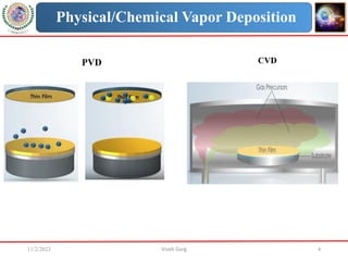
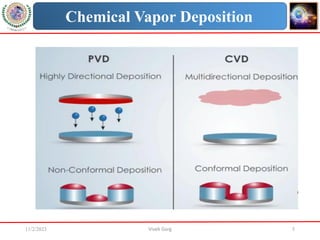
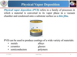
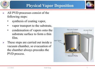
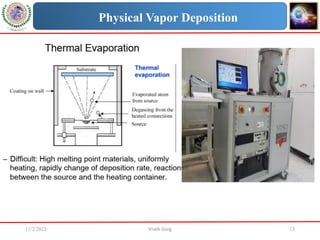
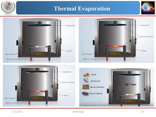
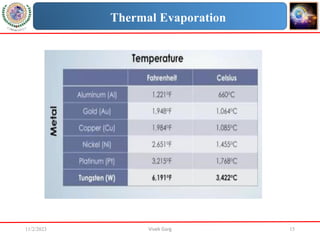
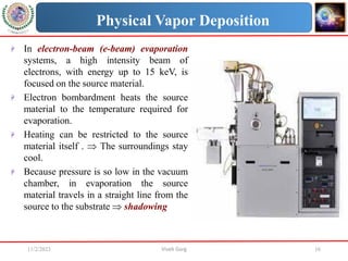
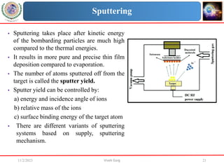
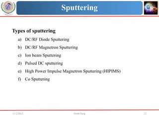
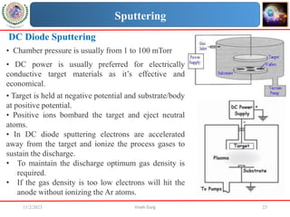
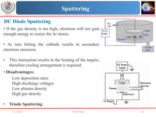
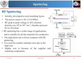
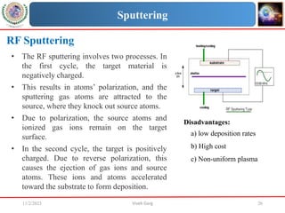
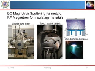
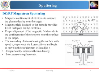
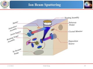
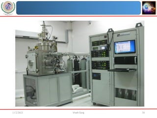
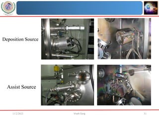
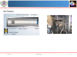
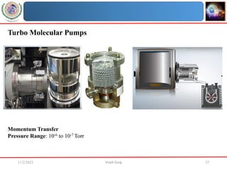
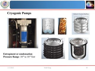
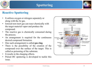
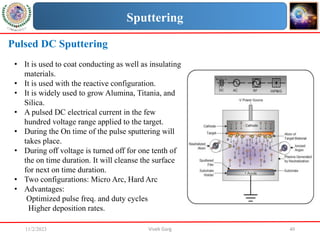
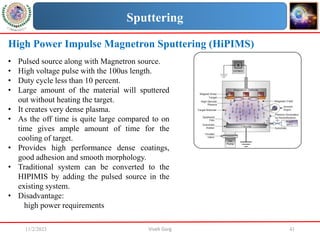
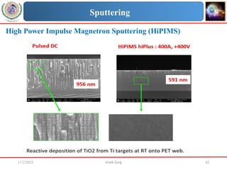
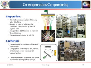
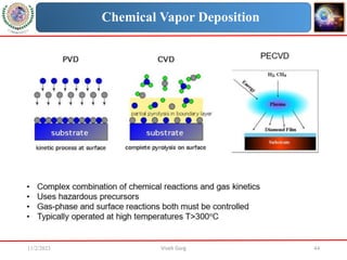
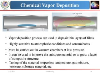
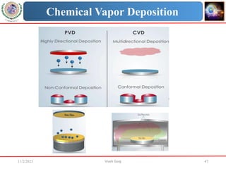
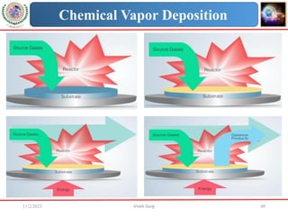
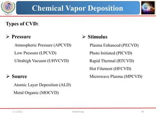
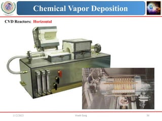
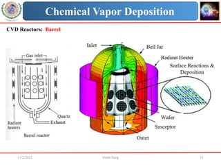
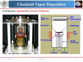
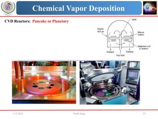
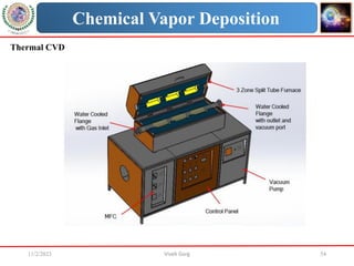
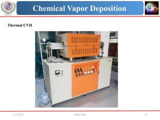
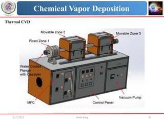
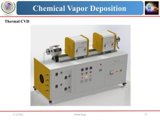
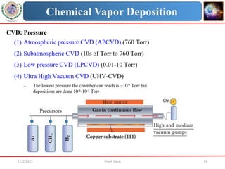
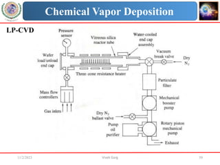
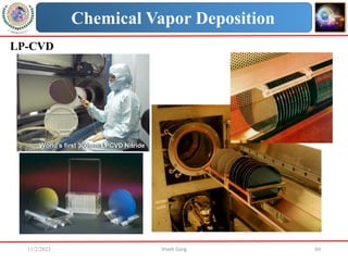
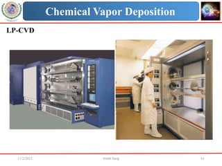
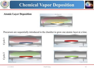
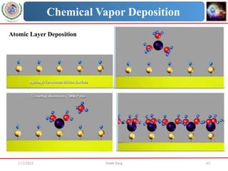
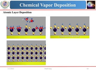
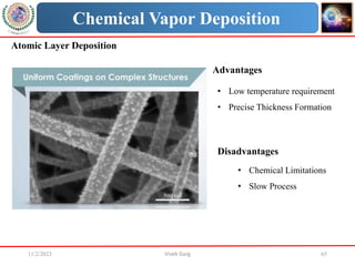
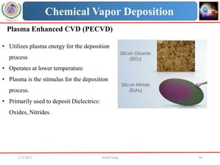
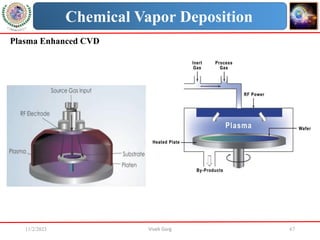
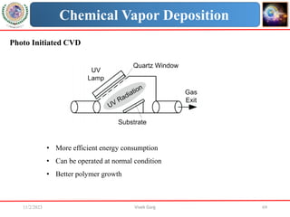
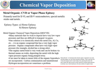
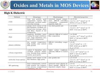
VLSI Technology
(EC 325)
Dr. Vivek Garg
Department of Electronics Engineering
S. V. National Institute of Technology (SVNIT)
Surat
email: vivekg@eced.svnit.ac.in; vivekgarg0101@gmail.com
11/2/2023 2
Course Outline
11/2/2023 3
Course Text and Materials
Additional:
• Relevant Journals and Conferences
• Materials and Sources shared in the lectures
11/2/2023 Vivek Garg 4
Physical/Chemical Vapor Deposition
PVD CVD
11/2/2023 Vivek Garg 5
Chemical Vapor Deposition
11/2/2023 Vivek Garg 6
Physical Vapor Deposition
Physical vapor deposition (PVD) refers to a family of processes in
which a material is converted to its vapor phase in a vacuum
chamber and condensed onto a substrate surface as a thin film.
PVD can be used to produce coatings of a wide variety of materials:
• metals alloys
• ceramics glasses
• semiconductors polymers
11/2/2023 Vivek Garg 7
Physical Vapor Deposition
 All PVD processes consist of the
following steps:
• synthesis of coating vapor,
• vapor transport to the substrate,
• condensation of vapors onto the
substrate surface to form a thin
film.
 These steps are carried out inside a
vacuum chamber, so evacuation of
the chamber always precedes the
PVD process.
11/2/2023 Vivek Garg 8
Thin Film Deposition
11/2/2023 Vivek Garg 9
Physical Vapor Deposition
 The two most common PVD processes are:
• Evaporation: Thermal, e-beam
• Sputtering
 For evaporation, the background pressure in the vacuum
chamber is typically ~10-6 Torr (~10-4 Pa) or lower.
 For sputtering, the background pressure in the vacuum
chamber is typically 10-3 to 10-2 Torr (~1 Pa).
11/2/2023 Vivek Garg 10
11/2/2023 Vivek Garg 11
11/2/2023 Vivek Garg 12
Evaporation
 In order to evaporate a material, it must be heated to a
temperature at which its vapor pressure is 10-3 Torr or higher.
 There are two common ways to heat the source material:
• resistive heating
• electron-beam heating.
 Resistive heating uses electric current flow through a tungsten
filament to heat the source material.
 The source material can be placed directly on the tungsten
filament, or it can be put in a crucible that is heated by the
filament.
11/2/2023 Vivek Garg 13
Physical Vapor Deposition
11/2/2023 Vivek Garg 14
Thermal Evaporation
11/2/2023 Vivek Garg 15
Thermal Evaporation
11/2/2023 Vivek Garg 16
Physical Vapor Deposition
 In electron-beam (e-beam) evaporation
systems, a high intensity beam of
electrons, with energy up to 15 keV, is
focused on the source material.
 Electron bombardment heats the source
material to the temperature required for
evaporation.
 Heating can be restricted to the source
material itself .  The surroundings stay
cool.
 Because pressure is so low in the vacuum
chamber, in evaporation the source
material travels in a straight line from the
source to the substrate  shadowing
11/2/2023 Vivek Garg 17
11/2/2023 Vivek Garg 18
11/2/2023 Vivek Garg 19
11/2/2023 Vivek Garg 20
Sputtering
11/2/2023 Vivek Garg 21
Sputtering
• Sputtering takes place after kinetic energy
of the bombarding particles are much high
compared to the thermal energies.
• It results in more pure and precise thin film
deposition compared to evaporation.
• The number of atoms sputtered off from the
target is called the sputter yield.
• Sputter yield can be controlled by:
a) energy and incidence angle of ions
b) relative mass of the ions
c) surface binding energy of the target atom
• There are different variants of sputtering
systems based on supply, sputtering
mechanism.
11/2/2023 Vivek Garg 22
Sputtering
Types of sputtering
a) DC/RF Diode Sputtering
b) DC/RF Magnetron Sputtering
c) Ion beam Sputtering
d) Pulsed DC sputtering
e) High Power Impulse Magnetron Sputtering (HIPIMS)
f) Co Sputtering
11/2/2023 Vivek Garg 23
DC Diode Sputtering
• Chamber pressure is usually from 1 to 100 mTorr
• DC power is usually preferred for electrically
conductive target materials as it’s effective and
economical.
• Target is held at negative potential and substrate/body
at positive potential.
• Positive ions bombard the target and eject neutral
atoms.
• In DC diode sputtering electrons are accelerated
away from the target and ionize the process gases to
sustain the discharge.
• To maintain the discharge optimum gas density is
required.
• If the gas density is too low electrons will hit the
anode without ionizing the Ar atoms.
Sputtering
11/2/2023 Vivek Garg 24
DC Diode Sputtering
• If the gas density is too high, electrons will not gain
enough energy to ionize the Ar atoms.
• Ar ions hitting the cathode results in secondary
electrons emission.
• This interaction results in the heating of the targets,
therefore cooling arrangement is required.
• Disadvantages:
Low deposition rates
High discharge voltages
Low plasma density
High gas density
• Triode Sputtering
Sputtering
11/2/2023 Vivek Garg 25
RF Sputtering
• Initially, developed to coat insulating layers.
• The power source is AC (13.6 MHz).
• RF peak to peak voltage is 1kV, electron
densities are 109 to 1011 cm-3, chamber pressure
0.5 to 10 mTorr.
• RF sputtering has a wider range of applications
and is suitable for all the materials for conductive
• The deposition rate is lower compare with DC
sputtering.
• It is used for smaller substrate sizes due to the
high cost.
• Higher cost is because of the supplies and
matching components.
Sputtering
11/2/2023 Vivek Garg 26
RF Sputtering
• The RF sputtering involves two processes. In
the first cycle, the target material is
negatively charged.
• This results in atoms’ polarization, and the
sputtering gas atoms are attracted to the
source, where they knock out source atoms.
• Due to polarization, the source atoms and
ionized gas ions remain on the target
surface.
• In the second cycle, the target is positively
charged. Due to reverse polarization, this
causes the ejection of gas ions and source
atoms. These ions and atoms accelerated
toward the substrate to form deposition.
Sputtering
Disadvantages:
a) low deposition rates
b) High cost
c) Non-uniform plasma
11/2/2023 Vivek Garg 27
11/2/2023 Vivek Garg 28
DC/RF Magnetron Sputtering
• Magnetic confinement of electrons to enhance
the plasma density near the target.
• Magnetic field is added to the cathode provides
E x B drift path for the electrons.
• Proper alignment of the magnetic field results in
the confinement of the electrons near the surface
of the target.
• The secondary electrons leaving the surface with
speed v, experience the Lorentz force and begin
to move in the circular path with radius r.
• It significantly increases the ion density.
• Low pressure requirements.
Sputtering
11/2/2023 Vivek Garg 29
Ion Beam Sputtering
11/2/2023 Vivek Garg 30
11/2/2023 Vivek Garg 31
 Deposition Source
Assist Source
Deposition Source
11/2/2023 Vivek Garg 32
 Deposition Source
Ion Source
11/2/2023 Vivek Garg 33
 Targets
 Vacuum Pump
 Sample Holder
 Robotic Arm
11/2/2023 Vivek Garg 34
11/2/2023 Vivek Garg 35
Pressure Gauge Turbo Pump
11/2/2023 Vivek Garg 36
Mechanical Pumps
Positive Displacement
Pressure Range: 1- 0.1 Torr
11/2/2023 Vivek Garg 37
Turbo Molecular Pumps
Momentum Transfer
Pressure Range: 10-6 to 10-7 Torr
11/2/2023 Vivek Garg 38
Cryogenic Pumps
Entrapment or condensation
Pressure Range: 10-8 to 10-9 Torr
11/2/2023 Vivek Garg 39
Reactive Sputtering
Sputtering
• It utilizes oxygen or nitrogen separately or
along with the Ar gas.
• Ionized non-inert gas can react chemically with
the target material vapor and produce the
compound.
• The reactive gas is chemically consumed during
the process.
• An arrangement is required for the continuous
desired compound formation.
• One such arrangement is called gas ring.
• There is the possibility of the creation of the
compound over the surface of the target. This is
called as poisoning of the substrate.
• It results in the charging effects.
• Pulsed DC sputtering is developed to tackle this
issue.
11/2/2023 Vivek Garg 40
Pulsed DC Sputtering
Sputtering
• It is used to coat conducting as well as insulating
materials.
• It is used with the reactive configuration.
• It is widely used to grow Alumina, Titania, and
Silica.
• A pulsed DC electrical current in the few
hundred voltage range applied to the target.
• During the On time of the pulse sputtering will
takes place.
• During off voltage is turned off for one tenth of
the on time duration. It will cleanse the surface
for next on time duration.
• Two configurations: Micro Arc, Hard Arc
• Advantages:
Optimized pulse freq. and duty cycles
Higher deposition rates.
11/2/2023 Vivek Garg 41
High Power Impulse Magnetron Sputtering (HiPIMS)
Sputtering
• Pulsed source along with Magnetron source.
• High voltage pulse with the 100us length.
• Duty cycle less than 10 percent.
• Large amount of the material will sputtered
out without heating the target.
• It creates very dense plasma.
• As the off time is quite large compared to on
time gives ample amount of time for the
cooling of target.
• Provides high performance dense coatings,
good adhesion and smooth morphology.
• Traditional system can be converted to the
HIPIMIS by adding the pulsed source in the
existing system.
• Disadvantage:
high power requirements
11/2/2023 Vivek Garg 42
High Power Impulse Magnetron Sputtering (HiPIMS)
Sputtering
11/2/2023 Vivek Garg 43
Co-evaporation/Co-sputtering
11/2/2023 Vivek Garg 44
Chemical Vapor Deposition
11/2/2023 Vivek Garg 45
11/2/2023 Vivek Garg 46
Chemical Vapor Deposition
• Vapor deposition process are used to deposit thin layers of films
• Highly sensitive to atmospheric conditions and contaminants.
• Must be carried out in vacuum chambers at low pressure.
• It can be used to improve the substrate material or to grow a layer
of composite structure.
• Tuning of the material properties: temperature, gas mixture,
pressure, substrate material, etc.
11/2/2023 Vivek Garg 47
Chemical Vapor Deposition
11/2/2023 Vivek Garg 48
Chemical Vapor Deposition
11/2/2023 Vivek Garg 49
Chemical Vapor Deposition
Types of CVD:
 Pressure
Atmospheric Pressure (APCVD)
Low Pressure (LPCVD)
Ultrahigh Vacuum (UHVCVD)
 Stimulus
Plasma Enhanced (PECVD)
Photo Initiated (PICVD)
Rapid Thermal (RTCVD)
Hot Filament (HFCVD)
Microwave Plasma (MPCVD)
 Source
Atomic Layer Deposition (ALD)
Metal Organic (MOCVD)
11/2/2023 Vivek Garg 50
Chemical Vapor Deposition
CVD Reactors: Horizontal
11/2/2023 Vivek Garg 51
Chemical Vapor Deposition
CVD Reactors: Barrel
11/2/2023 Vivek Garg 52
Chemical Vapor Deposition
CVD Reactors: Rotating Disk Vertical CVD Reactor
11/2/2023 Vivek Garg 53
Chemical Vapor Deposition
CVD Reactors: Pancake or Planetary
11/2/2023 Vivek Garg 54
Chemical Vapor Deposition
Thermal CVD
11/2/2023 Vivek Garg 55
Chemical Vapor Deposition
Thermal CVD
11/2/2023 Vivek Garg 56
Chemical Vapor Deposition
Thermal CVD
11/2/2023 Vivek Garg 57
Chemical Vapor Deposition
Thermal CVD
11/2/2023 Vivek Garg 58
Chemical Vapor Deposition
CVD: Pressure
11/2/2023 Vivek Garg 59
Chemical Vapor Deposition
LP-CVD
11/2/2023 Vivek Garg 60
Chemical Vapor Deposition
LP-CVD
11/2/2023 Vivek Garg 61
Chemical Vapor Deposition
LP-CVD
11/2/2023 Vivek Garg 62
Chemical Vapor Deposition
Atomic Layer Deposition
Precursors are sequentially introduced in the chamber to grow one atomic layer at a time.
Cycle
1
Cycle
2
11/2/2023 Vivek Garg 63
Chemical Vapor Deposition
Atomic Layer Deposition
11/2/2023 Vivek Garg 64
Chemical Vapor Deposition
Atomic Layer Deposition
11/2/2023 Vivek Garg 65
Chemical Vapor Deposition
Atomic Layer Deposition
• Low temperature requirement
• Precise Thickness Formation
Disadvantages
• Chemical Limitations
• Slow Process
Advantages
11/2/2023 Vivek Garg 66
Chemical Vapor Deposition
Plasma Enhanced CVD (PECVD)
• Utilizes plasma energy for the deposition
process
• Operates at lower temperature
• Plasma is the stimulus for the deposition
process.
• Primarily used to deposit Dielectrics:
Oxides, Nitrides.
11/2/2023 Vivek Garg 67
Chemical Vapor Deposition
Plasma Enhanced CVD
11/2/2023 Vivek Garg 68
Chemical Vapor Deposition
Microwave Plasma Enhanced CVD
• Microwaves are used to create
dense plasma.
• Substrate bias is applied.
• Widely used to create diamond
coatings.
11/2/2023 Vivek Garg 69
Chemical Vapor Deposition
Photo Initiated CVD
• More efficient energy consumption
• Can be operated at normal condition
• Better polymer growth
11/2/2023 Vivek Garg 70
Chemical Vapor Deposition
Metal Organic- CVD or Vapor Phase Epitaxy
Epitaxy Types: a) Homo Epitaxy
b) Hetero Epitaxy
11/2/2023 Vivek Garg 71
Chemical Vapor Deposition
Example Reaction:
Ga(CH3)3 + AsH3  3CH4 + GaAs
Trimethal
Gallium Gas
Arsene
Gas
Methane
Gas
on the
substrate
• The reaction occurs in a sealed container (reactor)
NOTE!! Arsene gas is highly toxic & highly flammable!
Trimethal gallium gas is highly toxic!!
Methane gas is highly explosive!
Chemical Vapor Deposition
11/2/2023 Vivek Garg 73
Chemical Vapor Deposition
Metal Organic CVD
11/2/2023 Vivek Garg 74
Oxides and Metals in MOS Devices
Silicon Dioxide
Deposition Processes
• LP CVD
• RF Sputtering
• Oxidation
11/2/2023 Vivek Garg 75
Oxides and Metals in MOS Devices
Poly Silicon
Deposition Processes
• LP CVD
• RF Sputtering
11/2/2023 Vivek Garg 76
Oxides and Metals in MOS Devices
Silicon Nitride
Deposition Processes
• PE CVD
• MOCVD
11/2/2023 Vivek Garg 77
Oxides and Metals in MOS Devices
High K Dielectric
11/2/2023 Vivek Garg 78
Oxides and Metals in MOS Devices
High K Dielectric
Deposition Processes
• ALD
• PE CVD
• MOCVD
• Pulsed Laser Deposition
• RF Sputtering
• E-Beam Evaporation
11/2/2023 Vivek Garg 79
Oxides and Metals in MOS Devices
High K Dielectric
11/2/2023 Vivek Garg 80
Oxides and Metals in MOS Devices
High K Dielectric

PVD-CVD..............................pdf

  • 1.
    VLSI Technology (EC 325) Dr.Vivek Garg Department of Electronics Engineering S. V. National Institute of Technology (SVNIT) Surat email: vivekg@eced.svnit.ac.in; vivekgarg0101@gmail.com
  • 2.
  • 3.
    11/2/2023 3 Course Textand Materials Additional: • Relevant Journals and Conferences • Materials and Sources shared in the lectures
  • 4.
    11/2/2023 Vivek Garg4 Physical/Chemical Vapor Deposition PVD CVD
  • 5.
    11/2/2023 Vivek Garg5 Chemical Vapor Deposition
  • 6.
    11/2/2023 Vivek Garg6 Physical Vapor Deposition Physical vapor deposition (PVD) refers to a family of processes in which a material is converted to its vapor phase in a vacuum chamber and condensed onto a substrate surface as a thin film. PVD can be used to produce coatings of a wide variety of materials: • metals alloys • ceramics glasses • semiconductors polymers
  • 7.
    11/2/2023 Vivek Garg7 Physical Vapor Deposition  All PVD processes consist of the following steps: • synthesis of coating vapor, • vapor transport to the substrate, • condensation of vapors onto the substrate surface to form a thin film.  These steps are carried out inside a vacuum chamber, so evacuation of the chamber always precedes the PVD process.
  • 8.
    11/2/2023 Vivek Garg8 Thin Film Deposition
  • 9.
    11/2/2023 Vivek Garg9 Physical Vapor Deposition  The two most common PVD processes are: • Evaporation: Thermal, e-beam • Sputtering  For evaporation, the background pressure in the vacuum chamber is typically ~10-6 Torr (~10-4 Pa) or lower.  For sputtering, the background pressure in the vacuum chamber is typically 10-3 to 10-2 Torr (~1 Pa).
  • 10.
  • 11.
  • 12.
    11/2/2023 Vivek Garg12 Evaporation  In order to evaporate a material, it must be heated to a temperature at which its vapor pressure is 10-3 Torr or higher.  There are two common ways to heat the source material: • resistive heating • electron-beam heating.  Resistive heating uses electric current flow through a tungsten filament to heat the source material.  The source material can be placed directly on the tungsten filament, or it can be put in a crucible that is heated by the filament.
  • 13.
    11/2/2023 Vivek Garg13 Physical Vapor Deposition
  • 14.
    11/2/2023 Vivek Garg14 Thermal Evaporation
  • 15.
    11/2/2023 Vivek Garg15 Thermal Evaporation
  • 16.
    11/2/2023 Vivek Garg16 Physical Vapor Deposition  In electron-beam (e-beam) evaporation systems, a high intensity beam of electrons, with energy up to 15 keV, is focused on the source material.  Electron bombardment heats the source material to the temperature required for evaporation.  Heating can be restricted to the source material itself .  The surroundings stay cool.  Because pressure is so low in the vacuum chamber, in evaporation the source material travels in a straight line from the source to the substrate  shadowing
  • 17.
  • 18.
  • 19.
  • 20.
    11/2/2023 Vivek Garg20 Sputtering
  • 21.
    11/2/2023 Vivek Garg21 Sputtering • Sputtering takes place after kinetic energy of the bombarding particles are much high compared to the thermal energies. • It results in more pure and precise thin film deposition compared to evaporation. • The number of atoms sputtered off from the target is called the sputter yield. • Sputter yield can be controlled by: a) energy and incidence angle of ions b) relative mass of the ions c) surface binding energy of the target atom • There are different variants of sputtering systems based on supply, sputtering mechanism.
  • 22.
    11/2/2023 Vivek Garg22 Sputtering Types of sputtering a) DC/RF Diode Sputtering b) DC/RF Magnetron Sputtering c) Ion beam Sputtering d) Pulsed DC sputtering e) High Power Impulse Magnetron Sputtering (HIPIMS) f) Co Sputtering
  • 23.
    11/2/2023 Vivek Garg23 DC Diode Sputtering • Chamber pressure is usually from 1 to 100 mTorr • DC power is usually preferred for electrically conductive target materials as it’s effective and economical. • Target is held at negative potential and substrate/body at positive potential. • Positive ions bombard the target and eject neutral atoms. • In DC diode sputtering electrons are accelerated away from the target and ionize the process gases to sustain the discharge. • To maintain the discharge optimum gas density is required. • If the gas density is too low electrons will hit the anode without ionizing the Ar atoms. Sputtering
  • 24.
    11/2/2023 Vivek Garg24 DC Diode Sputtering • If the gas density is too high, electrons will not gain enough energy to ionize the Ar atoms. • Ar ions hitting the cathode results in secondary electrons emission. • This interaction results in the heating of the targets, therefore cooling arrangement is required. • Disadvantages: Low deposition rates High discharge voltages Low plasma density High gas density • Triode Sputtering Sputtering
  • 25.
    11/2/2023 Vivek Garg25 RF Sputtering • Initially, developed to coat insulating layers. • The power source is AC (13.6 MHz). • RF peak to peak voltage is 1kV, electron densities are 109 to 1011 cm-3, chamber pressure 0.5 to 10 mTorr. • RF sputtering has a wider range of applications and is suitable for all the materials for conductive • The deposition rate is lower compare with DC sputtering. • It is used for smaller substrate sizes due to the high cost. • Higher cost is because of the supplies and matching components. Sputtering
  • 26.
    11/2/2023 Vivek Garg26 RF Sputtering • The RF sputtering involves two processes. In the first cycle, the target material is negatively charged. • This results in atoms’ polarization, and the sputtering gas atoms are attracted to the source, where they knock out source atoms. • Due to polarization, the source atoms and ionized gas ions remain on the target surface. • In the second cycle, the target is positively charged. Due to reverse polarization, this causes the ejection of gas ions and source atoms. These ions and atoms accelerated toward the substrate to form deposition. Sputtering Disadvantages: a) low deposition rates b) High cost c) Non-uniform plasma
  • 27.
  • 28.
    11/2/2023 Vivek Garg28 DC/RF Magnetron Sputtering • Magnetic confinement of electrons to enhance the plasma density near the target. • Magnetic field is added to the cathode provides E x B drift path for the electrons. • Proper alignment of the magnetic field results in the confinement of the electrons near the surface of the target. • The secondary electrons leaving the surface with speed v, experience the Lorentz force and begin to move in the circular path with radius r. • It significantly increases the ion density. • Low pressure requirements. Sputtering
  • 29.
    11/2/2023 Vivek Garg29 Ion Beam Sputtering
  • 30.
  • 31.
    11/2/2023 Vivek Garg31  Deposition Source Assist Source Deposition Source
  • 32.
    11/2/2023 Vivek Garg32  Deposition Source Ion Source
  • 33.
    11/2/2023 Vivek Garg33  Targets  Vacuum Pump  Sample Holder  Robotic Arm
  • 34.
  • 35.
    11/2/2023 Vivek Garg35 Pressure Gauge Turbo Pump
  • 36.
    11/2/2023 Vivek Garg36 Mechanical Pumps Positive Displacement Pressure Range: 1- 0.1 Torr
  • 37.
    11/2/2023 Vivek Garg37 Turbo Molecular Pumps Momentum Transfer Pressure Range: 10-6 to 10-7 Torr
  • 38.
    11/2/2023 Vivek Garg38 Cryogenic Pumps Entrapment or condensation Pressure Range: 10-8 to 10-9 Torr
  • 39.
    11/2/2023 Vivek Garg39 Reactive Sputtering Sputtering • It utilizes oxygen or nitrogen separately or along with the Ar gas. • Ionized non-inert gas can react chemically with the target material vapor and produce the compound. • The reactive gas is chemically consumed during the process. • An arrangement is required for the continuous desired compound formation. • One such arrangement is called gas ring. • There is the possibility of the creation of the compound over the surface of the target. This is called as poisoning of the substrate. • It results in the charging effects. • Pulsed DC sputtering is developed to tackle this issue.
  • 40.
    11/2/2023 Vivek Garg40 Pulsed DC Sputtering Sputtering • It is used to coat conducting as well as insulating materials. • It is used with the reactive configuration. • It is widely used to grow Alumina, Titania, and Silica. • A pulsed DC electrical current in the few hundred voltage range applied to the target. • During the On time of the pulse sputtering will takes place. • During off voltage is turned off for one tenth of the on time duration. It will cleanse the surface for next on time duration. • Two configurations: Micro Arc, Hard Arc • Advantages: Optimized pulse freq. and duty cycles Higher deposition rates.
  • 41.
    11/2/2023 Vivek Garg41 High Power Impulse Magnetron Sputtering (HiPIMS) Sputtering • Pulsed source along with Magnetron source. • High voltage pulse with the 100us length. • Duty cycle less than 10 percent. • Large amount of the material will sputtered out without heating the target. • It creates very dense plasma. • As the off time is quite large compared to on time gives ample amount of time for the cooling of target. • Provides high performance dense coatings, good adhesion and smooth morphology. • Traditional system can be converted to the HIPIMIS by adding the pulsed source in the existing system. • Disadvantage: high power requirements
  • 42.
    11/2/2023 Vivek Garg42 High Power Impulse Magnetron Sputtering (HiPIMS) Sputtering
  • 43.
    11/2/2023 Vivek Garg43 Co-evaporation/Co-sputtering
  • 44.
    11/2/2023 Vivek Garg44 Chemical Vapor Deposition
  • 45.
  • 46.
    11/2/2023 Vivek Garg46 Chemical Vapor Deposition • Vapor deposition process are used to deposit thin layers of films • Highly sensitive to atmospheric conditions and contaminants. • Must be carried out in vacuum chambers at low pressure. • It can be used to improve the substrate material or to grow a layer of composite structure. • Tuning of the material properties: temperature, gas mixture, pressure, substrate material, etc.
  • 47.
    11/2/2023 Vivek Garg47 Chemical Vapor Deposition
  • 48.
    11/2/2023 Vivek Garg48 Chemical Vapor Deposition
  • 49.
    11/2/2023 Vivek Garg49 Chemical Vapor Deposition Types of CVD:  Pressure Atmospheric Pressure (APCVD) Low Pressure (LPCVD) Ultrahigh Vacuum (UHVCVD)  Stimulus Plasma Enhanced (PECVD) Photo Initiated (PICVD) Rapid Thermal (RTCVD) Hot Filament (HFCVD) Microwave Plasma (MPCVD)  Source Atomic Layer Deposition (ALD) Metal Organic (MOCVD)
  • 50.
    11/2/2023 Vivek Garg50 Chemical Vapor Deposition CVD Reactors: Horizontal
  • 51.
    11/2/2023 Vivek Garg51 Chemical Vapor Deposition CVD Reactors: Barrel
  • 52.
    11/2/2023 Vivek Garg52 Chemical Vapor Deposition CVD Reactors: Rotating Disk Vertical CVD Reactor
  • 53.
    11/2/2023 Vivek Garg53 Chemical Vapor Deposition CVD Reactors: Pancake or Planetary
  • 54.
    11/2/2023 Vivek Garg54 Chemical Vapor Deposition Thermal CVD
  • 55.
    11/2/2023 Vivek Garg55 Chemical Vapor Deposition Thermal CVD
  • 56.
    11/2/2023 Vivek Garg56 Chemical Vapor Deposition Thermal CVD
  • 57.
    11/2/2023 Vivek Garg57 Chemical Vapor Deposition Thermal CVD
  • 58.
    11/2/2023 Vivek Garg58 Chemical Vapor Deposition CVD: Pressure
  • 59.
    11/2/2023 Vivek Garg59 Chemical Vapor Deposition LP-CVD
  • 60.
    11/2/2023 Vivek Garg60 Chemical Vapor Deposition LP-CVD
  • 61.
    11/2/2023 Vivek Garg61 Chemical Vapor Deposition LP-CVD
  • 62.
    11/2/2023 Vivek Garg62 Chemical Vapor Deposition Atomic Layer Deposition Precursors are sequentially introduced in the chamber to grow one atomic layer at a time. Cycle 1 Cycle 2
  • 63.
    11/2/2023 Vivek Garg63 Chemical Vapor Deposition Atomic Layer Deposition
  • 64.
    11/2/2023 Vivek Garg64 Chemical Vapor Deposition Atomic Layer Deposition
  • 65.
    11/2/2023 Vivek Garg65 Chemical Vapor Deposition Atomic Layer Deposition • Low temperature requirement • Precise Thickness Formation Disadvantages • Chemical Limitations • Slow Process Advantages
  • 66.
    11/2/2023 Vivek Garg66 Chemical Vapor Deposition Plasma Enhanced CVD (PECVD) • Utilizes plasma energy for the deposition process • Operates at lower temperature • Plasma is the stimulus for the deposition process. • Primarily used to deposit Dielectrics: Oxides, Nitrides.
  • 67.
    11/2/2023 Vivek Garg67 Chemical Vapor Deposition Plasma Enhanced CVD
  • 68.
    11/2/2023 Vivek Garg68 Chemical Vapor Deposition Microwave Plasma Enhanced CVD • Microwaves are used to create dense plasma. • Substrate bias is applied. • Widely used to create diamond coatings.
  • 69.
    11/2/2023 Vivek Garg69 Chemical Vapor Deposition Photo Initiated CVD • More efficient energy consumption • Can be operated at normal condition • Better polymer growth
  • 70.
    11/2/2023 Vivek Garg70 Chemical Vapor Deposition Metal Organic- CVD or Vapor Phase Epitaxy Epitaxy Types: a) Homo Epitaxy b) Hetero Epitaxy
  • 71.
    11/2/2023 Vivek Garg71 Chemical Vapor Deposition Example Reaction: Ga(CH3)3 + AsH3  3CH4 + GaAs Trimethal Gallium Gas Arsene Gas Methane Gas on the substrate • The reaction occurs in a sealed container (reactor) NOTE!! Arsene gas is highly toxic & highly flammable! Trimethal gallium gas is highly toxic!! Methane gas is highly explosive!
  • 72.
  • 73.
    11/2/2023 Vivek Garg73 Chemical Vapor Deposition Metal Organic CVD
  • 74.
    11/2/2023 Vivek Garg74 Oxides and Metals in MOS Devices Silicon Dioxide Deposition Processes • LP CVD • RF Sputtering • Oxidation
  • 75.
    11/2/2023 Vivek Garg75 Oxides and Metals in MOS Devices Poly Silicon Deposition Processes • LP CVD • RF Sputtering
  • 76.
    11/2/2023 Vivek Garg76 Oxides and Metals in MOS Devices Silicon Nitride Deposition Processes • PE CVD • MOCVD
  • 77.
    11/2/2023 Vivek Garg77 Oxides and Metals in MOS Devices High K Dielectric
  • 78.
    11/2/2023 Vivek Garg78 Oxides and Metals in MOS Devices High K Dielectric Deposition Processes • ALD • PE CVD • MOCVD • Pulsed Laser Deposition • RF Sputtering • E-Beam Evaporation
  • 79.
    11/2/2023 Vivek Garg79 Oxides and Metals in MOS Devices High K Dielectric
  • 80.
    11/2/2023 Vivek Garg80 Oxides and Metals in MOS Devices High K Dielectric