Downloaded 2,087 times


This document summarizes a seminar on sputtering processes. Sputtering is a thin film deposition technique where atoms are ejected from a target material when bombarded by energetic particles in vacuum. The ejected atoms then deposit onto a substrate to form a thin film. Key aspects of sputtering discussed include sputtering yield, how various parameters like ion mass, energy and pressure affect the process, and applications in microelectronics, decorative coatings, and medical devices.
Introduction to sputtering and thin films; outline of topics covered including applications and methods.
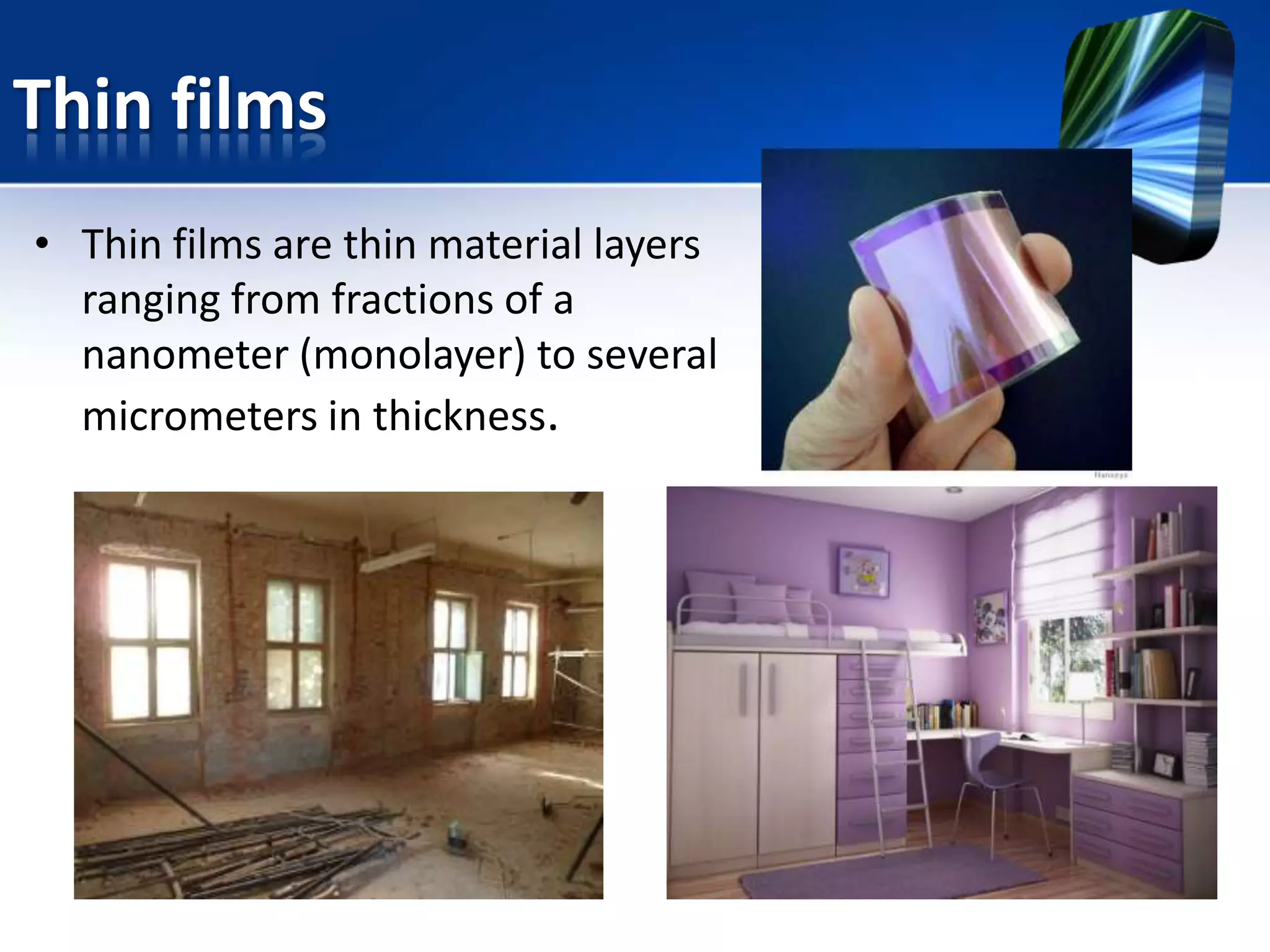
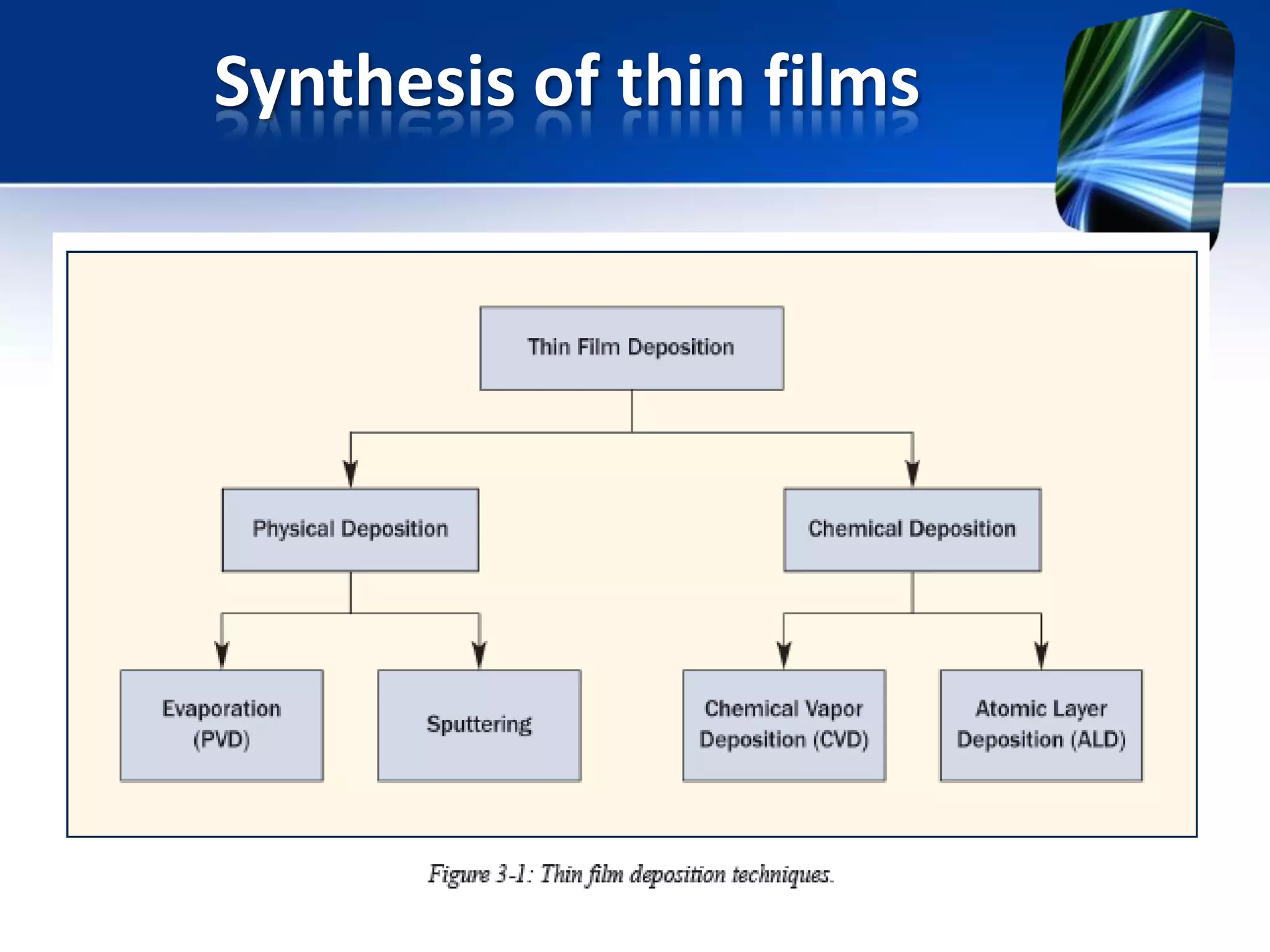
Definition and basic characteristics of thin films; synthesis overview.
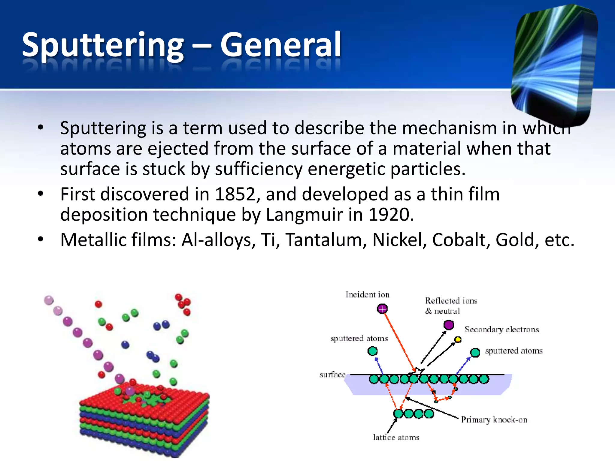
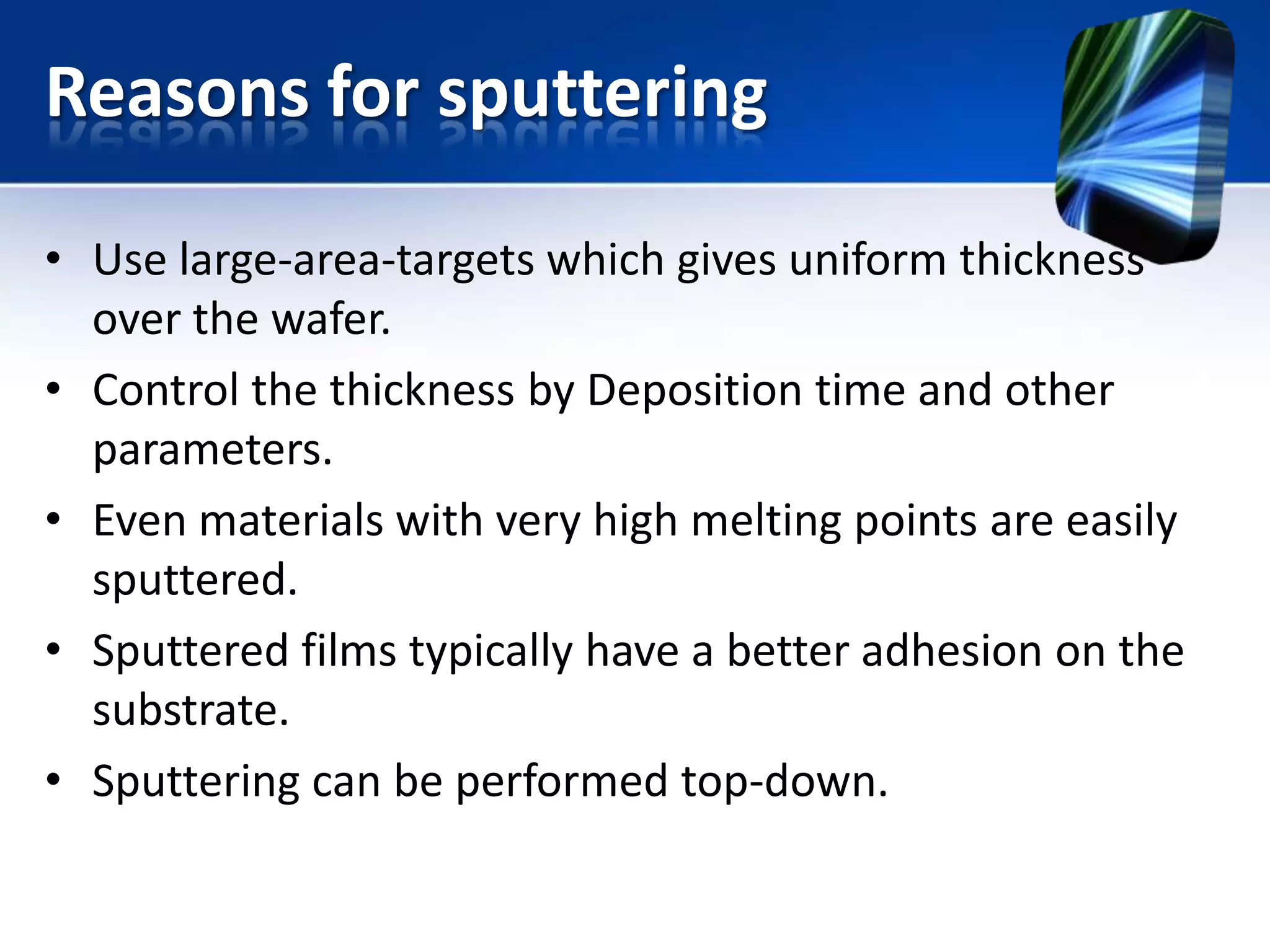
Overview of sputtering mechanism, its discovery, metallic films, and advantages for uniformity and adhesion.
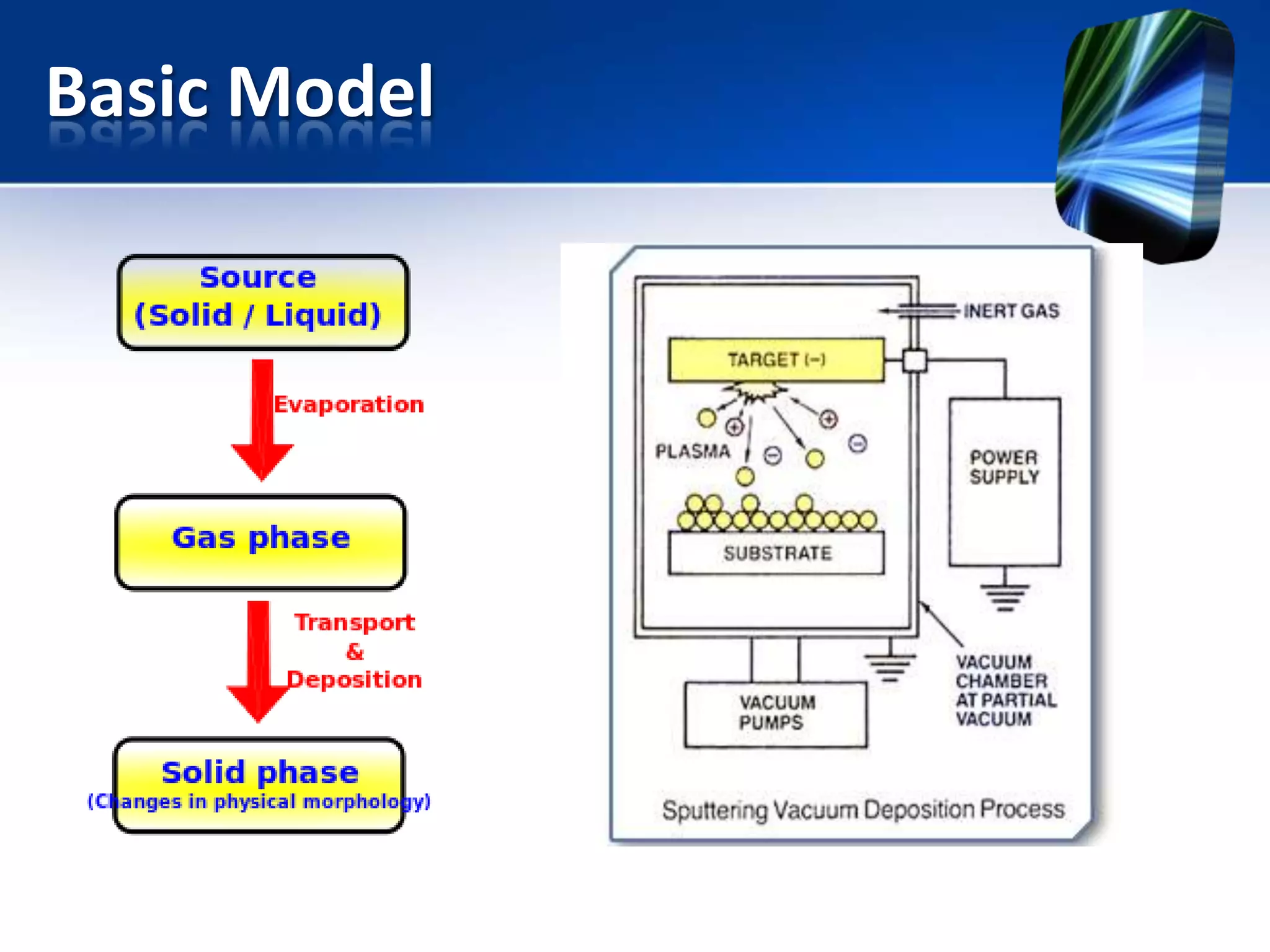
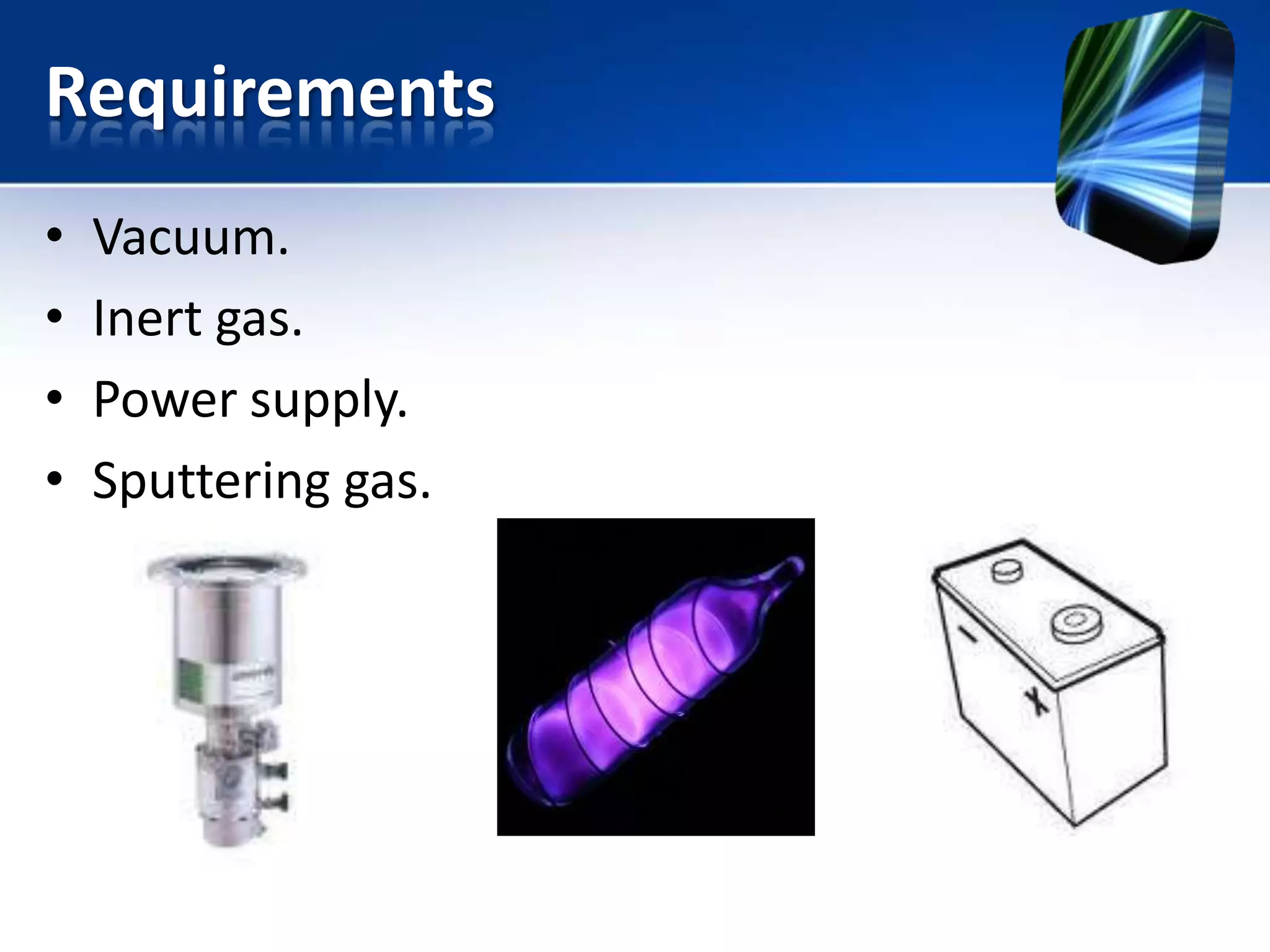
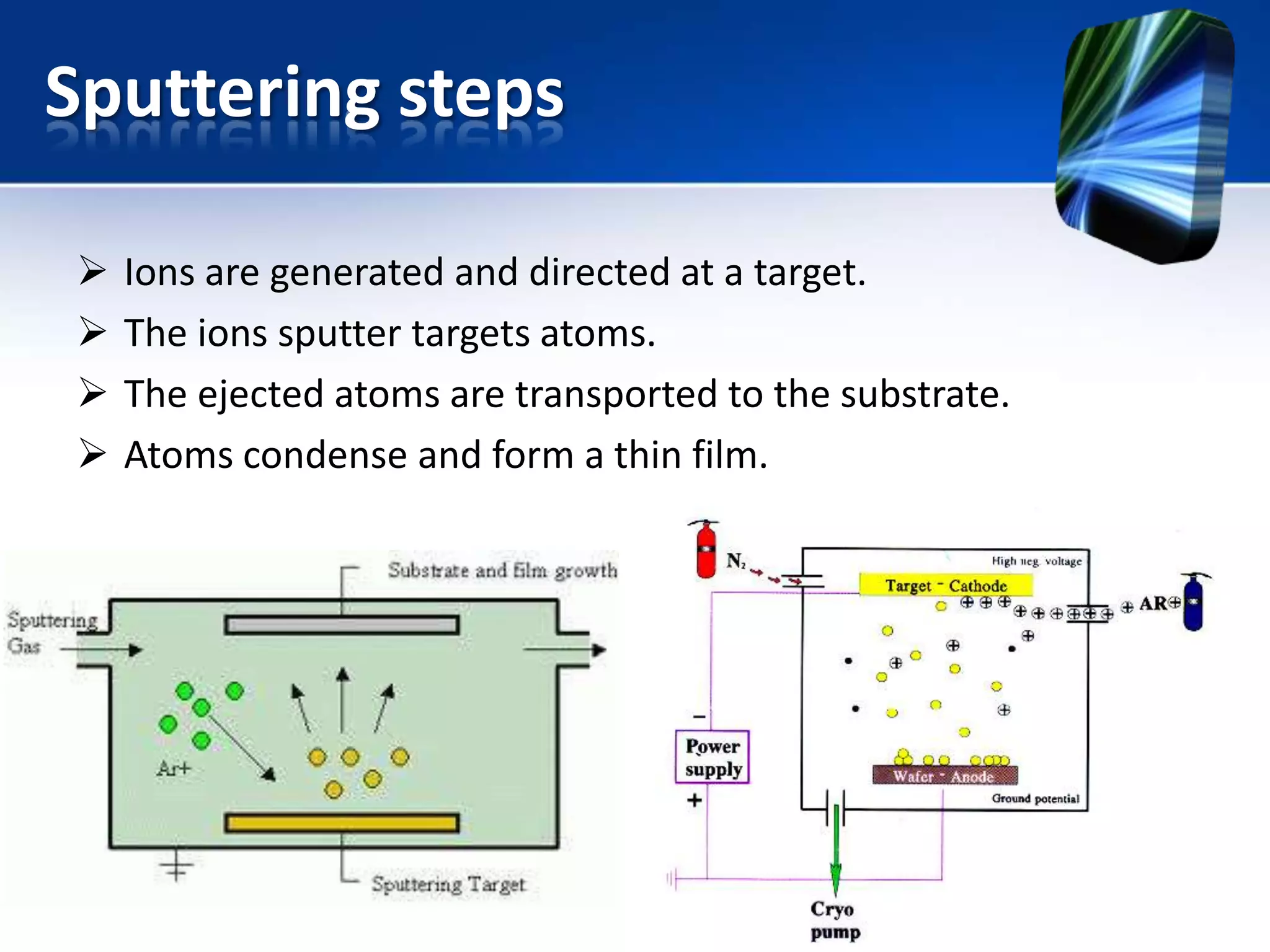
Basic model of sputtering; requirements like vacuum and gas; detailed steps of the sputtering process.
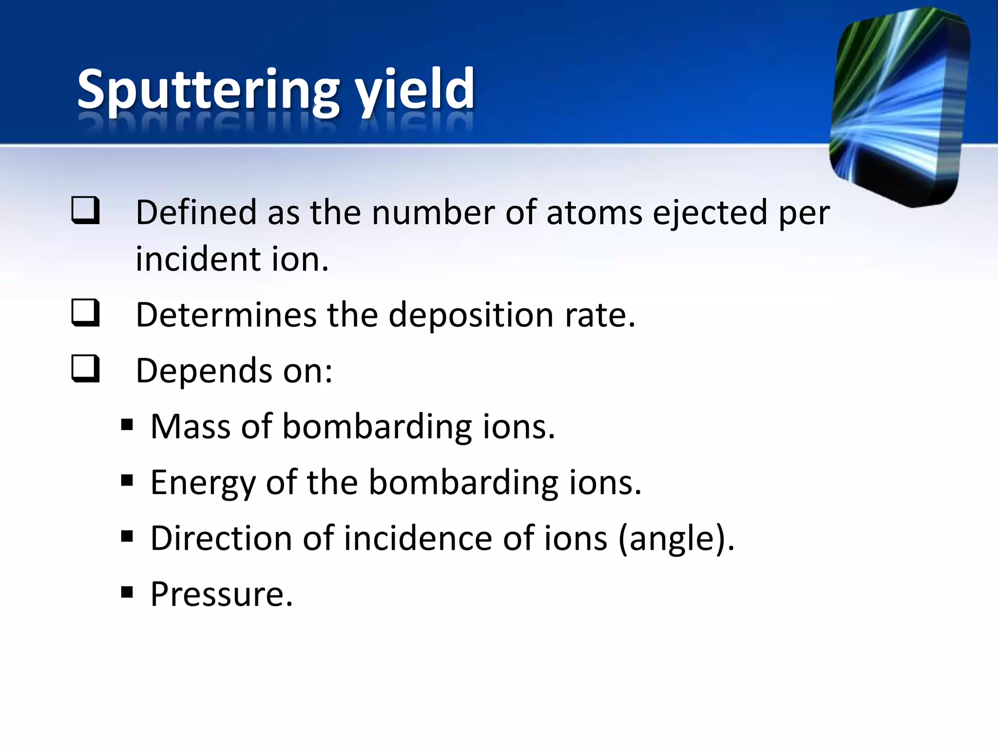
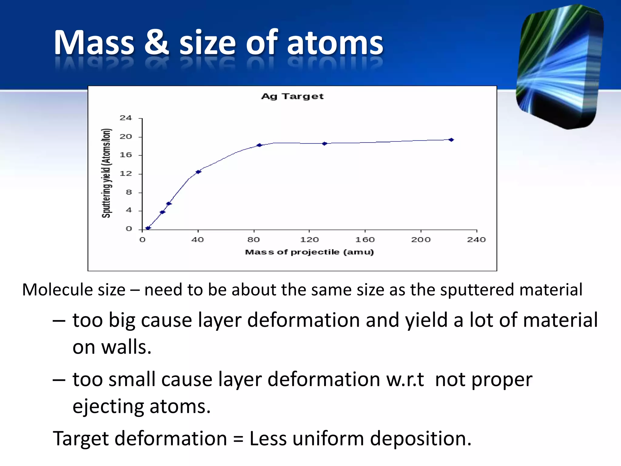
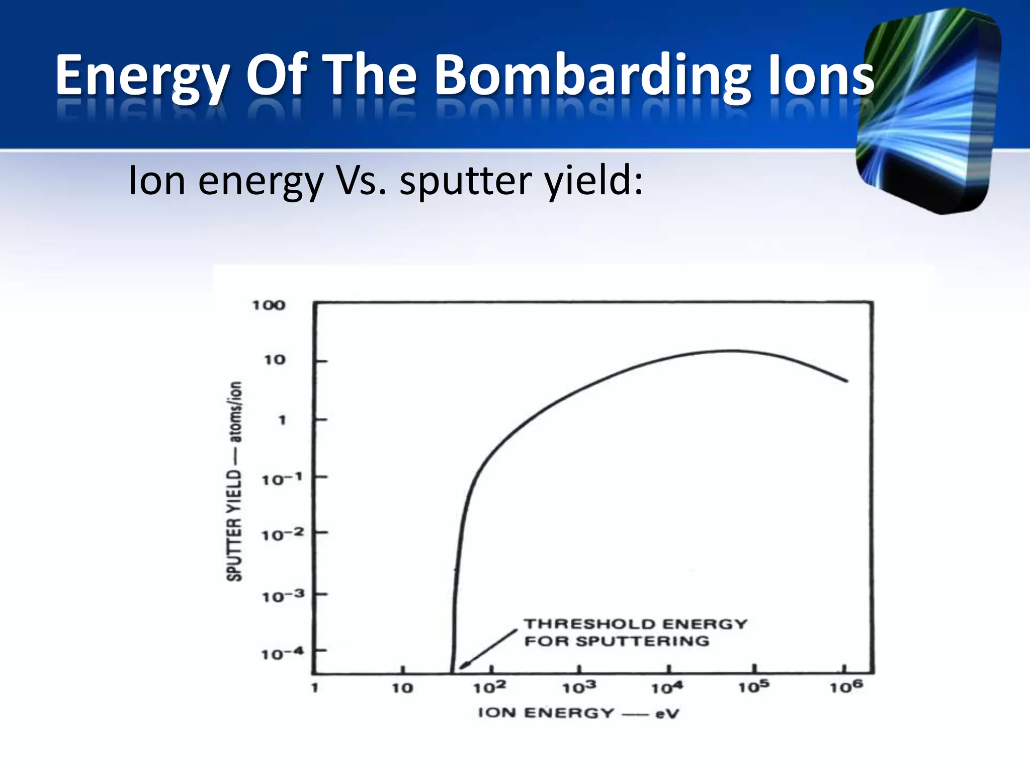
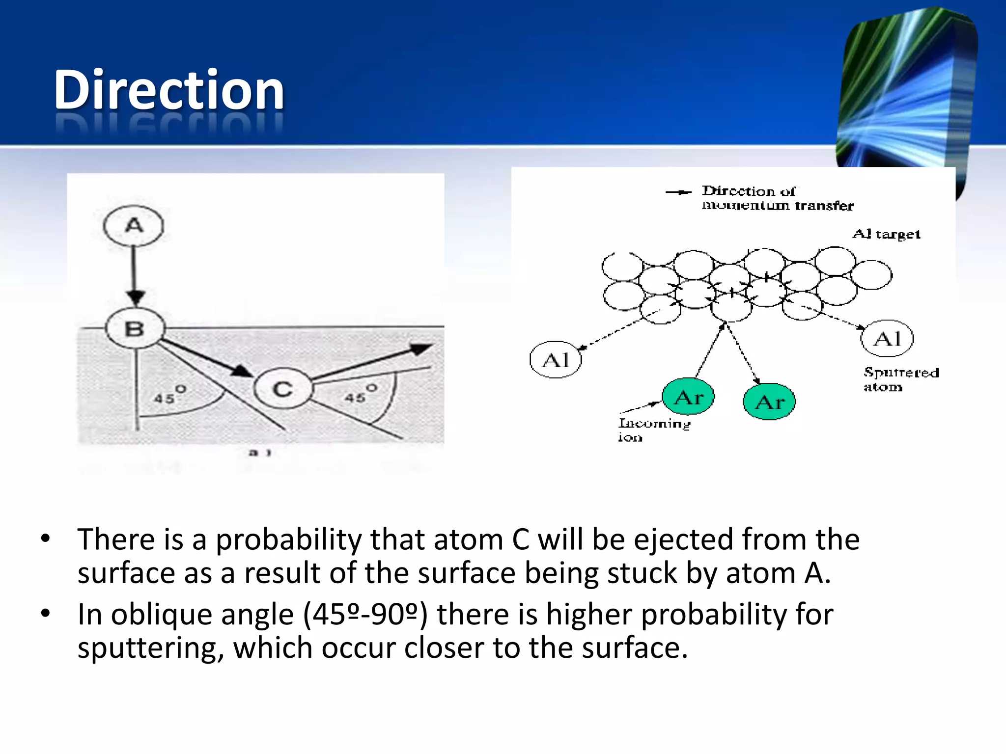
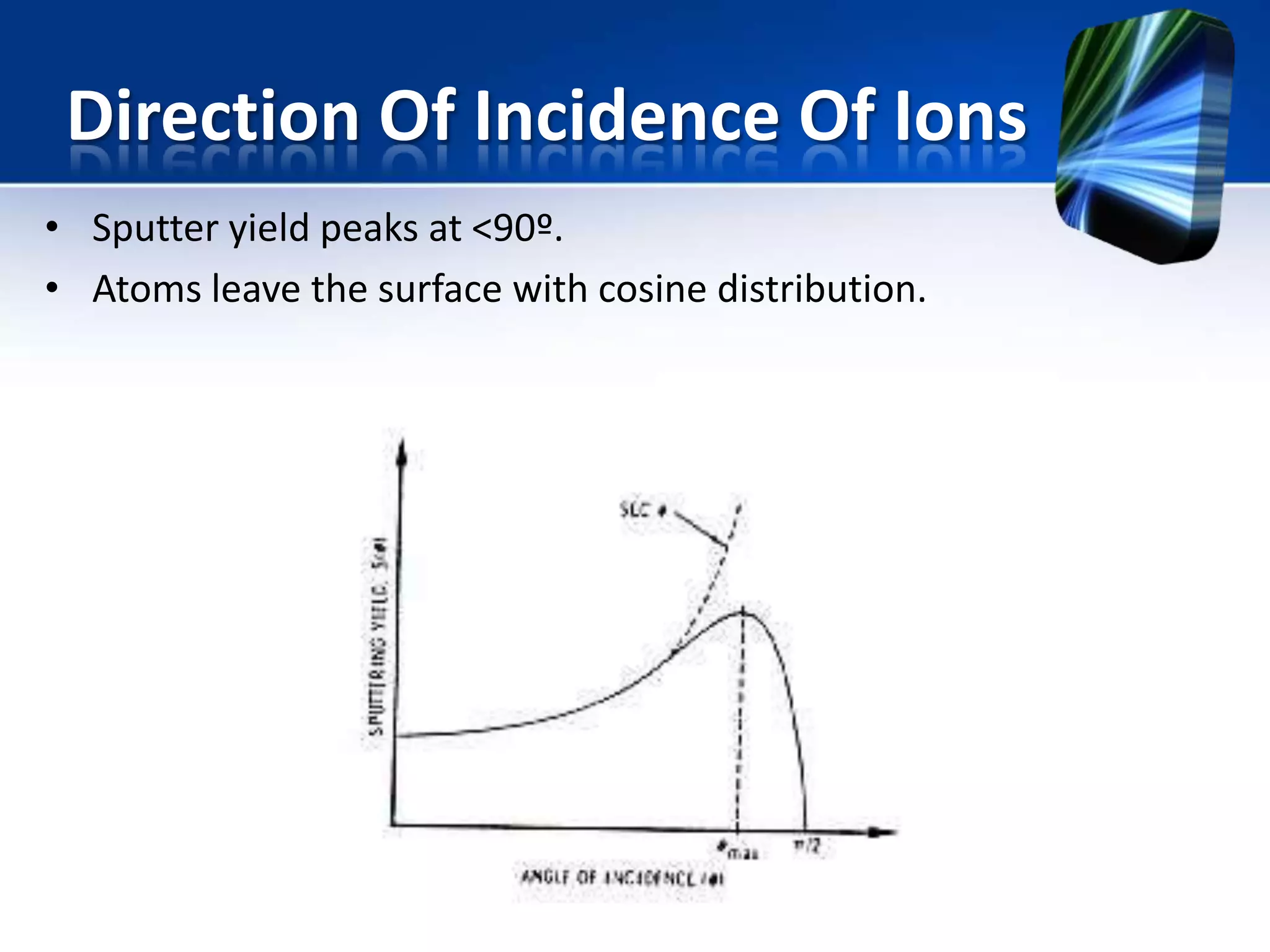
Factors influencing sputtering yield: mass and size of atoms, energy of ions, angle, and pressure effects.
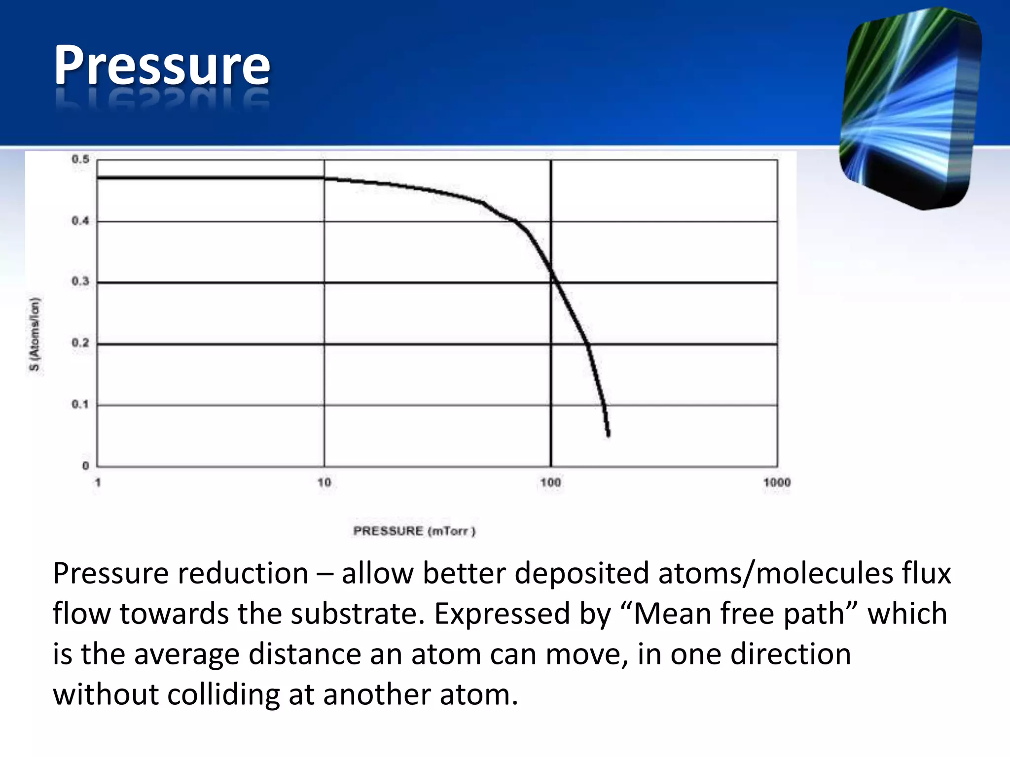
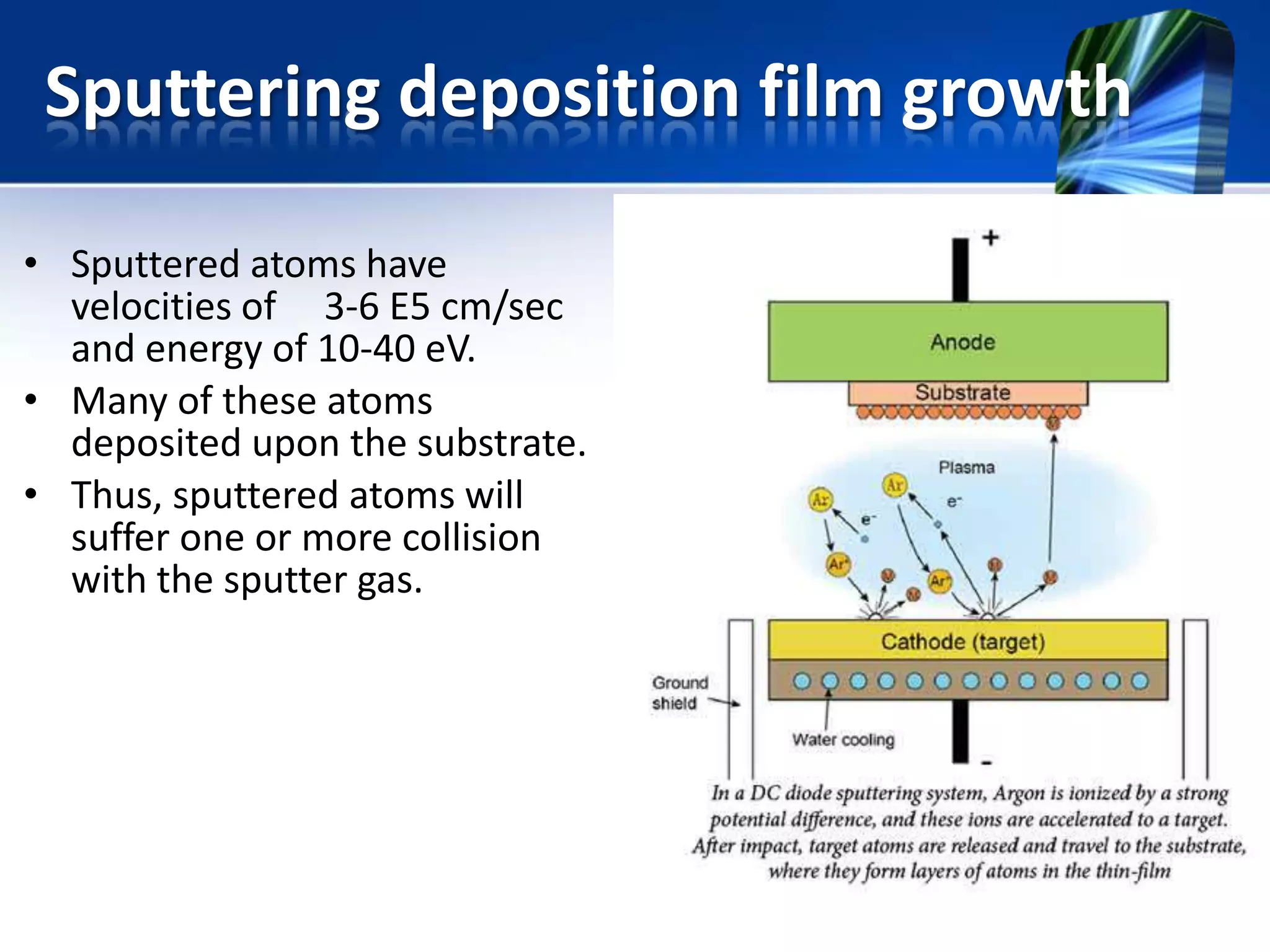
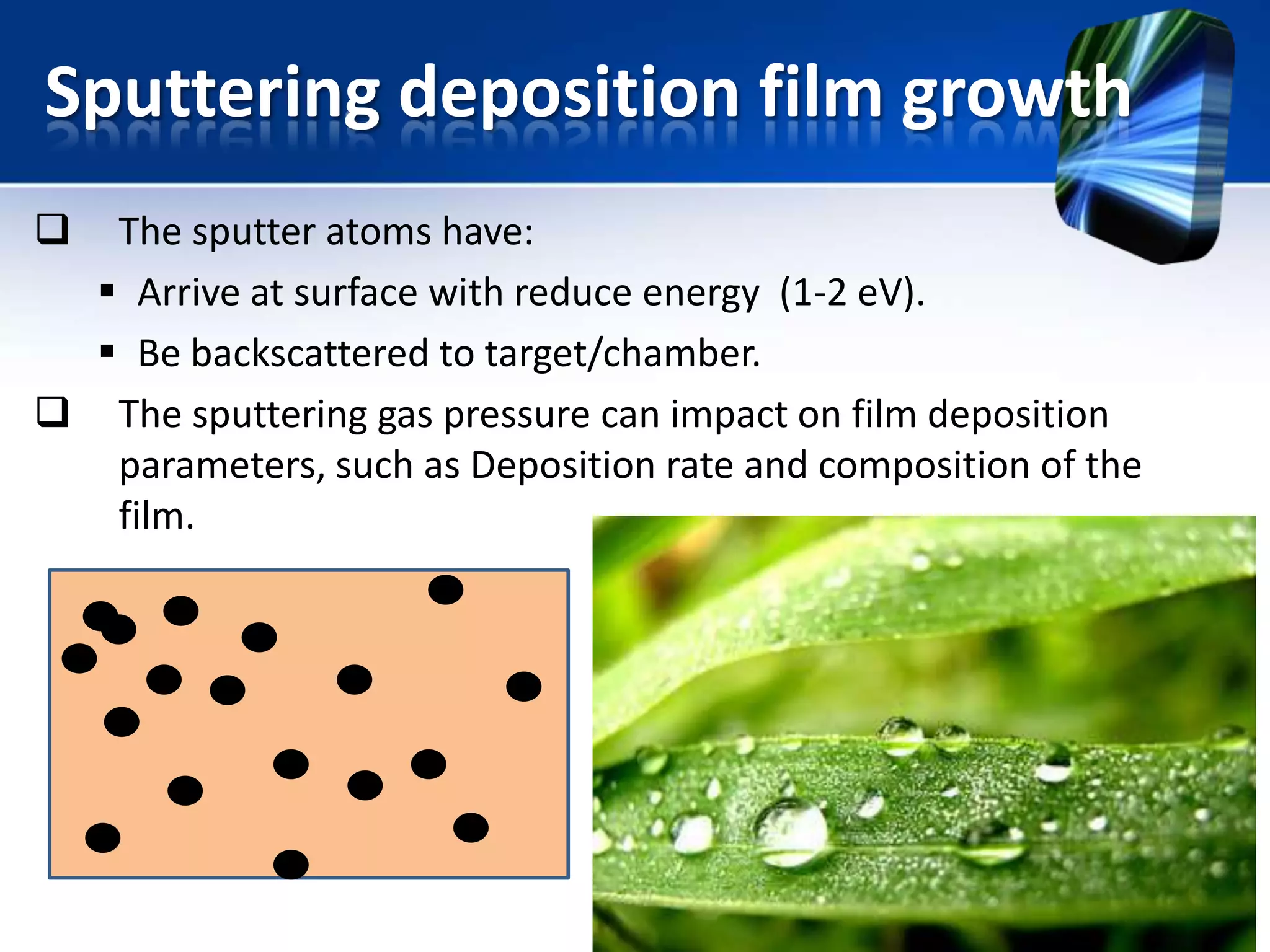
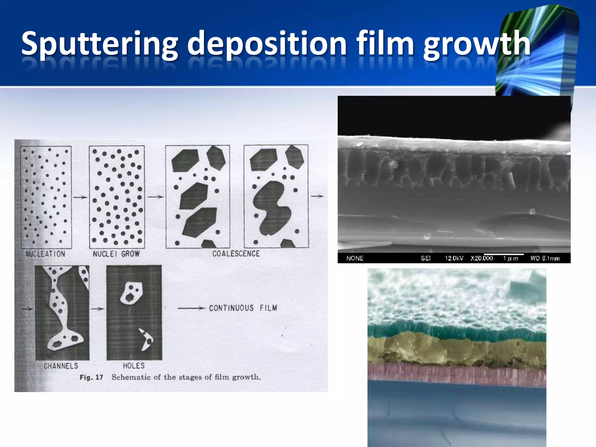
Kinetics of film growth; impact of atom velocity, energy, and gas pressure on deposition.
Various applications of sputtering including thin film deposition, etching, and surface treatment.
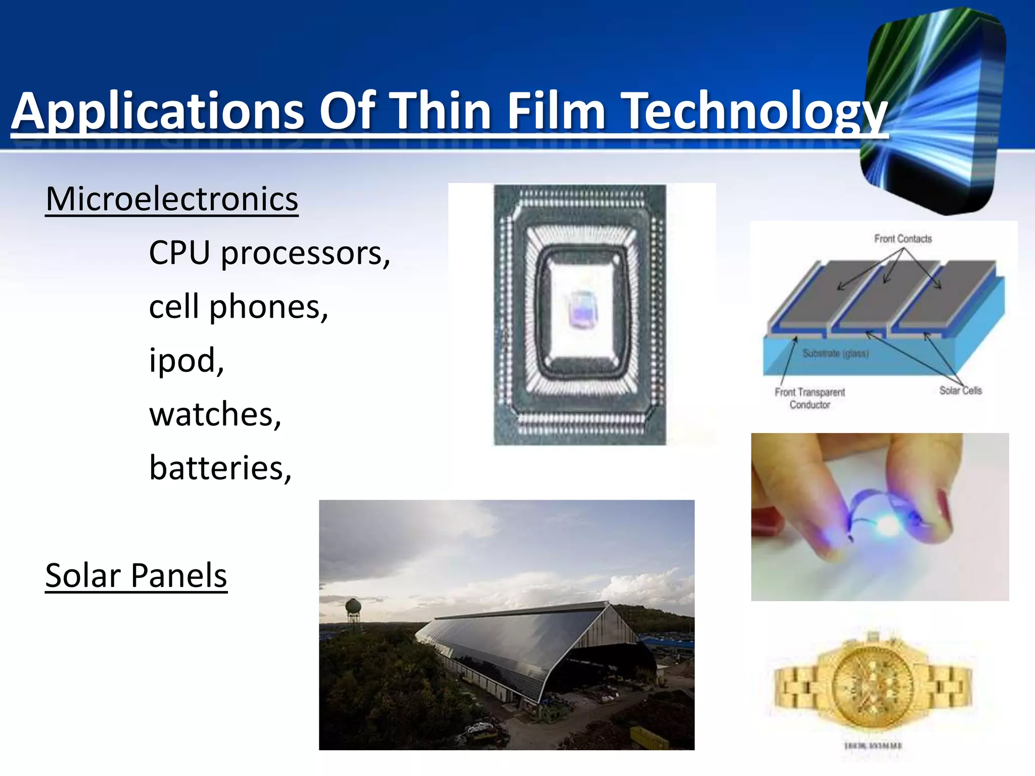
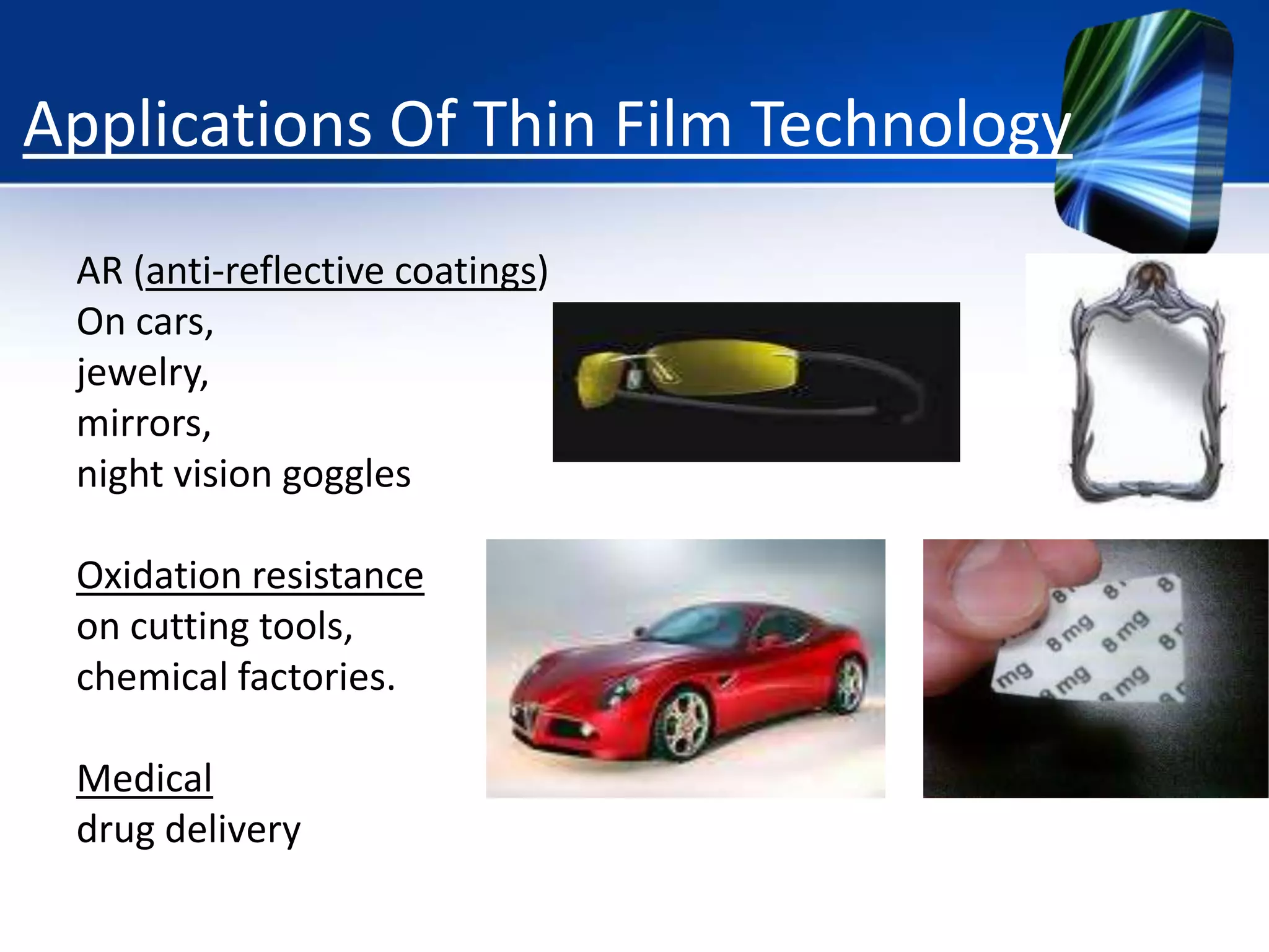
Diverse applications of thin film technology in microelectronics, protective coatings, and medical fields.
Supplementary video resources and references for deeper understanding of thin film deposition techniques.


![Thin_Film_Technology_introduction[1]](https://cdn.slidesharecdn.com/ss_thumbnails/1b4496c8-2102-411b-8465-a3dd3f398327-150205034538-conversion-gate02-thumbnail.jpg?width=640&height=640&fit=bounds)


