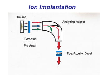
Ion Implantation - Semiconductor manufaturing technology
1.
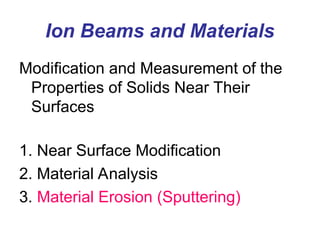
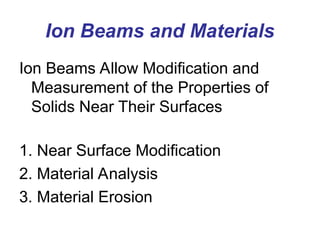
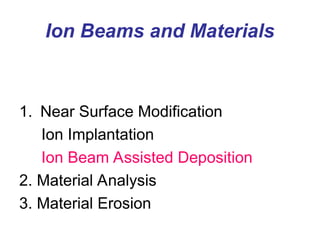
Ion Beams andMaterials
Ion Beams Allow Modification and
Measurement of the Properties of
Solids Near Their Surfaces
1. Near Surface Modification
2. Material Analysis
3. Material Erosion
2.
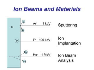
Ion Beams andMaterials
Ar+
1 keV
P+
100 keV
He+
1 MeV
Si
Sputtering
Ion
Implantation
Ion Beam
Analysis
P
Si
Si
He
He
The Boron Manufacturing
Problem
AsMOS device dimensions shrink with each
new generation of devices:
1. The energy of the implanted ions must
be decreased to reduce their range
2. The number of implanted ions must be
increased to increase the volume
concentration
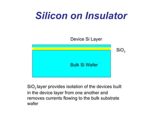
Silicon on Insulator
SiO2
DeviceSi Layer
Bulk Si Wafer
SiO2 layer provides isolation of the devices built
in the device layer from one another and
removes currents flowing to the bulk substrate
wafer
Schematic flow ofSmart
Cut process
Initial
Initial Silicon
Silicon
Oxidation
Oxidation
Smart
Smart Cut
Cut
Implantation
Implantation
Cleaning
Cleaning &
&
Bonding
Bonding
Splitting
Splitting
Annealing
Annealing &
&
Finishing
Finishing
Re
Re-
-use of A
use of A
or B
or B New A
New A New B
New B
A
A
B
B
A
A
A
A
H
H+
+ ions
ions
SOI wafer
SOI wafer
Si
Si bulk
bulk
A
A
B
B
A
A
B
B
Or
Or
New A
New A New B
New B
A
A
B
B
B
B
A
A
A
A
H
H+
+ ions
ions
SOI wafer
SOI wafer
Si
Si bulk
bulk
Si
Si bulk
bulk
A
A
B
B
A
A
B
B
B
B
Or
Or
Soitec Corp
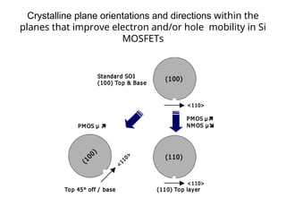
16.
Crystalline plane orientationsand directions within the
planes that improve electron and/or hole mobility in Si
MOSFETs
(100)
(100)
<110>
Standard SOI
(100) Top & Base
(
1
0
0
)
(
1
0
0
)
<
1
1
0
>
Top 45° off / base
PMOS µ
(110)
(110)
<110>
PMOS µ
NMOS µ
(110) Top layer
(100)
(100)
<110>
(100)
(100)
<110>
Standard SOI
(100) Top & Base
(
1
0
0
)
(
1
0
0
)
<
1
1
0
>
(
1
0
0
)
(
1
0
0
)
<
1
1
0
>
Top 45° off / base
PMOS µ
(110)
(110)
<110>
PMOS µ
NMOS µ
(110) Top layer
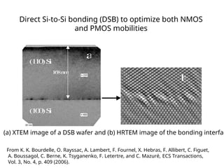
17.
Direct Si-to-Si bonding(DSB) to optimize both NMOS
and PMOS mobilities
(1
1
0
)S
i
(1
0
0
)S
i
a
b
1
6
8n
m
From K. K. Bourdelle, O. Rayssac, A. Lambert, F. Fournel, X. Hebras, F. Allibert, C. Figuet,
A. Boussagol, C. Berne, K. Tsyganenko, F. Letertre, and C. Mazuré, ECS Transactions,
Vol. 3, No. 4, p. 409 (2006).
(a) XTEM image of a DSB wafer and (b) HRTEM image of the bonding interfac
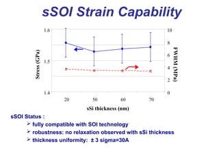
18.
Stress
(GPa)
FWHM
(MPa)
sSi thickness (nm)
1.4
1.5
1.6
2050 60 70
0
2
4
6
8
10
sSOI Status :
fully compatible with SOI technology
robustness: no relaxation observed with sSi thickness
thickness uniformity: ± 3 sigma=30A
sSOI Strain Capability
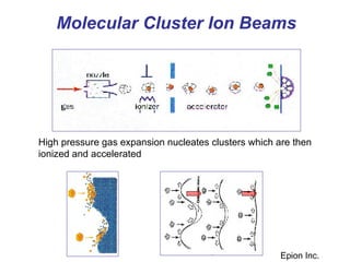
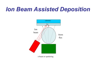
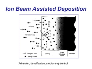
Ion Beam AssistedDeposition
Adhesion, densification, stociometry control
27.
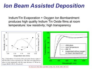
Ion Beam AssistedDeposition
Indium/Tin Evaporation + Oxygen Ion Bombardment
produces high quality Indium Tin Oxide films at room
temperature: low resistivity; high transparency
28.
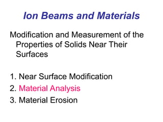
Ion Beams andMaterials
Modification and Measurement of the
Properties of Solids Near Their
Surfaces
1. Near Surface Modification
2. Material Analysis
3. Material Erosion
29.
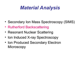
Material Analysis
• SecondaryIon Mass Spectroscopy (SIMS)
• Rutherford Backscattering
• Resonant Nuclear Scattering
• Ion Induced X-ray Spectroscopy
• Ion Produced Secondary Electron
Microscopy
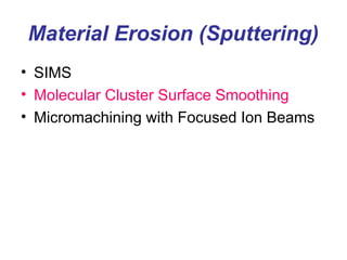
Ion Beams andMaterials
Modification and Measurement of the
Properties of Solids Near Their
Surfaces
1. Near Surface Modification
2. Material Analysis
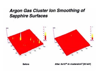
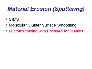
3. Material Erosion (Sputtering)
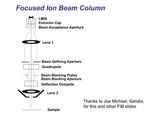
Beam Defining Aperture
Quadrupole
LMIS
ExtractorCap
Beam Acceptance Aperture
Lens 1
Lens 2
Beam Blanking Plates
Beam Blanking Aperture
Deflection Octopole
Sample
Focused Ion Beam Column
Thanks to Joe Michael, Sandia,
for this and other FIB slides
38.
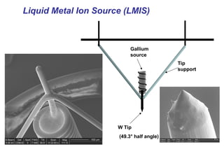
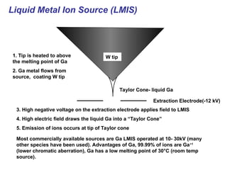
Liquid Metal IonSource (LMIS)
Gallium
source
W Tip
(49.3° half angle)
Tip
support
39.
Liquid Metal IonSource (LMIS)
W tip
Taylor Cone- liquid Ga
Extraction Electrode(-12 kV)
1. Tip is heated to above
the melting point of Ga
2. Ga metal flows from
source, coating W tip
3. High negative voltage on the extraction electrode applies field to LMIS
4. High electric field draws the liquid Ga into a “Taylor Cone”
5. Emission of ions occurs at tip of Taylor cone
Most commercially available sources are Ga LMIS operated at 10- 30kV (many
other species have been used). Advantages of Ga, 99.99% of ions are Ga+1
(lower chromatic aberration), Ga has a low melting point of 30°C (room temp
source).
40.
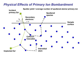
Physical Effects ofPrimary Ion Bombardment
Implanted Ga+
Incident
primary Ga+
Collision
Cascades
Sputtered
species
Sputter yield = average number of sputtered atoms/ primary ion
Sample
surface
Interstitial
atom
e-
e-
e-
e-
Secondary
electrons
41.
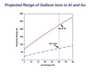
0
50
100
150
200
250
300
5 10 1520 25 30 35 40
Projected
Range
(A)
Ion Energy (kV)
Ga in Al
Ga in Au
Projected Range of Gallium Ions in Al and Au
42.
Ion Beam
Electron Beam
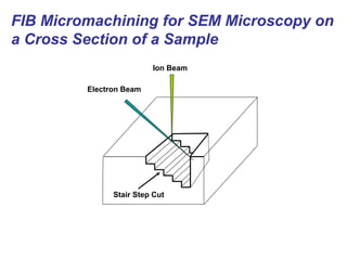
FIBMicromachining for SEM Microscopy on
a Cross Section of a Sample
Stair Step Cut
43.
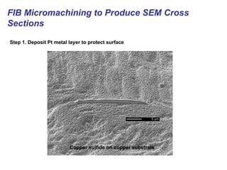
FIB Micromachining toProduce SEM Cross
Sections
Copper sulfide on copper substrate
Step 1. Deposit Pt metal layer to protect surface
44.
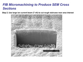
FIB Micromachining toProduce SEM Cross
Sections
Step 2. Use large ion current beam (7 nA) to cut rough staircase near area interest
45.
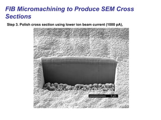
FIB Micromachining toProduce SEM Cross
Sections
Step 3. Polish cross section using lower ion beam current (1000 pA),
46.
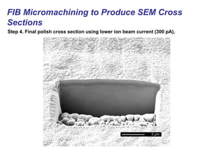
FIB Micromachining toProduce SEM Cross
Sections
Step 4. Final polish cross section using lower ion beam current (300 pA),
47.
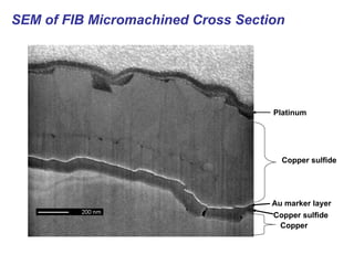
SEM of FIBMicromachined Cross Section
Platinum
Copper sulfide
Au marker layer
Copper sulfide
Copper
48.
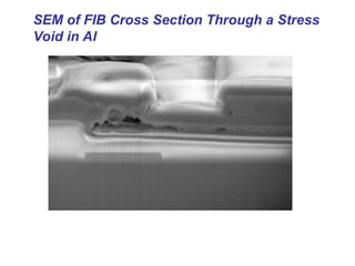
SEM of FIBCross Section Through a Stress
Void in Al
49.
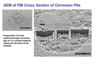
SEM of FIBCross Section of Corrosion Pits
Preparation of cross
section through corrosion
pits on Cu contact material
allows pit structure to be
studied.
50.
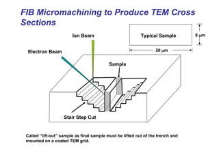
FIB Micromachining toProduce TEM Cross
Sections
8 m
Stair Step Cut
Ion Beam
Electron Beam
Sample
Called “lift-out” sample as final sample must be lifted out of the trench and
mounted on a coated TEM grid.
Typical Sample
20 m
51.
FIB Micromachining toProduce TEM Cross
Sections
Step 4. Polish both sides of cross section using lower ion beam current (1000 pA) to
about 1 m thickness,
500 pA beam size
300 nA beam size
52.
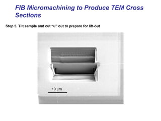
FIB Micromachining toProduce TEM Cross
Sections
Step 5. Tilt sample and cut “u” out to prepare for lift-out
53.
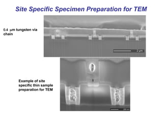
Site Specific SpecimenPreparation for TEM
Example of site
specific thin sample
preparation for TEM
m tungsten via
chain
54.
Material Analysis
• SecondaryIon Mass Spectroscopy (SIMS)
• Rutherford Backscattering
• Resonant Nuclear Scattering
• Ion Induced X-ray Spectroscopy
• Ion Produced Secondary Electron
Microscopy
55.
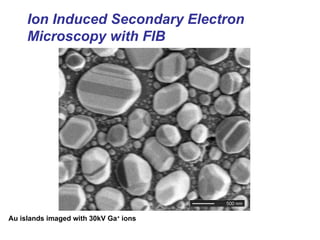
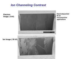
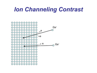
Ion Induced SecondaryElectron
Microscopy with FIB
Au islands imaged with 30kV Ga+
ions
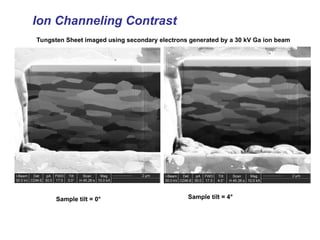
Ion Channeling Contrast
TungstenSheet imaged using secondary electrons generated by a 30 kV Ga ion beam
Sample tilt = 0° Sample tilt = 4°
59.
SUMMARY
Ions of differentatoms, molecules and
atomic clusters and having energies
between 1 keV and 3 MeV are highly
effective in modifying and measuring the
composition and structure of materials
close to their surfaces. This field has
developed over the last 50 years and
continues to evolve year after year as new
applications are recognized and new
techniques are developed.
61.
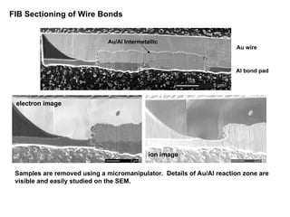
FIB Sectioning ofWire Bonds
Samples are removed using a micromanipulator. Details of Au/Al reaction zone are
visible and easily studied on the SEM.
electron image
ion image
Au wire
Al bond pad
Au/Al Intermetallic
62.
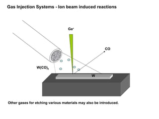
Gas Injection Systems- Ion beam induced reactions
W(CO)6
Ga+
CO
W
Other gases for etching various materials may also be introduced.
63.
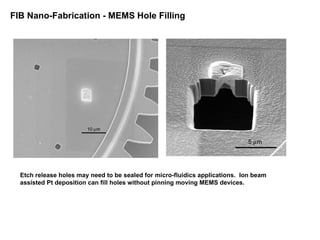
FIB Nano-Fabrication -MEMS Hole Filling
Etch release holes may need to be sealed for micro-fluidics applications. Ion beam
assisted Pt deposition can fill holes without pinning moving MEMS devices.


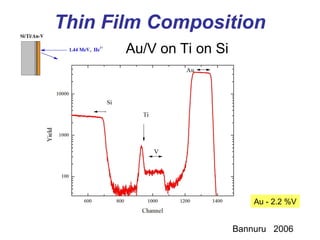
![Rutherford Backscatting
He+
Larger target
element mass =
larger K. For
1800
scattering
K= [(M-4)/(M+4)]2
KAu = 0 .92
KV = 0.73
KTi = 0.71](https://image.slidesharecdn.com/ionimplantation-250606035523-21ea1f38/85/Ion-Implantation-Semiconductor-manufaturing-technology-30-320.jpg)