1) The document describes programming the on-chip 10-bit ADC of the LPC2148 microcontroller to implement a simple data acquisition system. It discusses the features of the ADC, the programming interface, control registers, and provides code to initialize the ADC and read conversion results.
2) The code configures the ADC ports and control registers, reads the conversion results when the ADC status indicates a conversion is complete, and prints the voltage levels to the UART.
3) The results show the ADC accurately converts analog voltages from 0-3.1V to their corresponding 10-bit digital values, which are printed to the UART terminal.
this ppt only for beginner who want to understand concept of Timer counter operation of LPC2148 step by step.
hope it may help u.
always welcoming ur suggestion.
Defuzzification is the process of producing a quantifiable result in Crisp logic, given fuzzy sets and corresponding membership degrees. It is the process that maps a fuzzy set to a crisp set. It is typically needed in fuzzy control systems.
This presentation discusses the basics of Pass Transistor Logic, its advantages, limitation and finally implementation of Boolean functions/Combinational Logic circuits using Pass Transistor Logic.
THIS DESCRIBES VARIOUS ELEMENTS OF TRANSPORT PROTOCOL IN TRANSPORT LAYER OF COMPUTER NETWORKS
THERE ARE SIX ELEMENTS OF TRANSPORT PROTOCOL NAMELY
1. ADDRESSING
2. CONNECTION ESTABLISHMENT
3.CONNECTION REFUSE
4.FLOW CONTROL AND BUFFERS
5.MULTIPLEXING
6.CRASH RECOVERY
Salient Features:
The magnitude response is nearly constant(equal to 1) at lower frequencies
There are no ripples in passband and stop band
The maximum gain occurs at Ω=0 and it is H(Ω)=1
The magnitude response is monotonically decreasing
As the order of the filter ‘N’ increases, the response of the filter is more close to the ideal response
This presentation givens an overview of interfacing of a real tie clock IC with 8051. The contents are referred from book of mazidi.
Also an internal architecture of an RTC is given for reference.
An analog-to-digital converter (ADC, A/D, or A to D) is a device that converts a continuous physical quantity (usually voltage) to a digital number that represents the quantity's amplitude.
The conversion involves quantization of the input, so it necessarily introduces a small amount of error. Instead of doing a single conversion, an ADC often performs the conversions ("samples" the input) periodically. The result is a sequence of digital values that have been converted from a continuous-time and continuous-amplitude analog signal to a discrete-time and discrete-amplitude digital signal.
Searching for Embedded Systems,VLSI,Matlab, PLC scada Training Institute in Hyderabad-Get the Best Embedded Systems,VLSI,Matlab, PLC scada Training with Real time Projects from Nanocdac. Register now for new batches Call Us-040 -23754144,+91- 9640648777
Analog-to-Digital Converter (ADC) is an integral part of high-speed signal processing applications. This paper discusses about 10-bit SAR based ADC that enables very low power consumption and sampling rate as high as 165 MSPS.
Similar to Analog To Digital Conversion (ADC) Programming in LPC2148 (20)
Saudi Arabia stands as a titan in the global energy landscape, renowned for its abundant oil and gas resources. It's the largest exporter of petroleum and holds some of the world's most significant reserves. Let's delve into the top 10 oil and gas projects shaping Saudi Arabia's energy future in 2024.
CFD Simulation of By-pass Flow in a HRSG module by R&R Consult.pptxR&R Consult
CFD analysis is incredibly effective at solving mysteries and improving the performance of complex systems!
Here's a great example: At a large natural gas-fired power plant, where they use waste heat to generate steam and energy, they were puzzled that their boiler wasn't producing as much steam as expected.
R&R and Tetra Engineering Group Inc. were asked to solve the issue with reduced steam production.
An inspection had shown that a significant amount of hot flue gas was bypassing the boiler tubes, where the heat was supposed to be transferred.
R&R Consult conducted a CFD analysis, which revealed that 6.3% of the flue gas was bypassing the boiler tubes without transferring heat. The analysis also showed that the flue gas was instead being directed along the sides of the boiler and between the modules that were supposed to capture the heat. This was the cause of the reduced performance.
Based on our results, Tetra Engineering installed covering plates to reduce the bypass flow. This improved the boiler's performance and increased electricity production.
It is always satisfying when we can help solve complex challenges like this. Do your systems also need a check-up or optimization? Give us a call!
Work done in cooperation with James Malloy and David Moelling from Tetra Engineering.
More examples of our work https://www.r-r-consult.dk/en/cases-en/
Cosmetic shop management system project report.pdfKamal Acharya
Buying new cosmetic products is difficult. It can even be scary for those who have sensitive skin and are prone to skin trouble. The information needed to alleviate this problem is on the back of each product, but it's thought to interpret those ingredient lists unless you have a background in chemistry.
Instead of buying and hoping for the best, we can use data science to help us predict which products may be good fits for us. It includes various function programs to do the above mentioned tasks.
Data file handling has been effectively used in the program.
The automated cosmetic shop management system should deal with the automation of general workflow and administration process of the shop. The main processes of the system focus on customer's request where the system is able to search the most appropriate products and deliver it to the customers. It should help the employees to quickly identify the list of cosmetic product that have reached the minimum quantity and also keep a track of expired date for each cosmetic product. It should help the employees to find the rack number in which the product is placed.It is also Faster and more efficient way.
Student information management system project report ii.pdfKamal Acharya
Our project explains about the student management. This project mainly explains the various actions related to student details. This project shows some ease in adding, editing and deleting the student details. It also provides a less time consuming process for viewing, adding, editing and deleting the marks of the students.
Sachpazis:Terzaghi Bearing Capacity Estimation in simple terms with Calculati...Dr.Costas Sachpazis
Terzaghi's soil bearing capacity theory, developed by Karl Terzaghi, is a fundamental principle in geotechnical engineering used to determine the bearing capacity of shallow foundations. This theory provides a method to calculate the ultimate bearing capacity of soil, which is the maximum load per unit area that the soil can support without undergoing shear failure. The Calculation HTML Code included.
NO1 Uk best vashikaran specialist in delhi vashikaran baba near me online vas...Amil Baba Dawood bangali
Contact with Dawood Bhai Just call on +92322-6382012 and we'll help you. We'll solve all your problems within 12 to 24 hours and with 101% guarantee and with astrology systematic. If you want to take any personal or professional advice then also you can call us on +92322-6382012 , ONLINE LOVE PROBLEM & Other all types of Daily Life Problem's.Then CALL or WHATSAPP us on +92322-6382012 and Get all these problems solutions here by Amil Baba DAWOOD BANGALI
#vashikaranspecialist #astrologer #palmistry #amliyaat #taweez #manpasandshadi #horoscope #spiritual #lovelife #lovespell #marriagespell#aamilbabainpakistan #amilbabainkarachi #powerfullblackmagicspell #kalajadumantarspecialist #realamilbaba #AmilbabainPakistan #astrologerincanada #astrologerindubai #lovespellsmaster #kalajaduspecialist #lovespellsthatwork #aamilbabainlahore#blackmagicformarriage #aamilbaba #kalajadu #kalailam #taweez #wazifaexpert #jadumantar #vashikaranspecialist #astrologer #palmistry #amliyaat #taweez #manpasandshadi #horoscope #spiritual #lovelife #lovespell #marriagespell#aamilbabainpakistan #amilbabainkarachi #powerfullblackmagicspell #kalajadumantarspecialist #realamilbaba #AmilbabainPakistan #astrologerincanada #astrologerindubai #lovespellsmaster #kalajaduspecialist #lovespellsthatwork #aamilbabainlahore #blackmagicforlove #blackmagicformarriage #aamilbaba #kalajadu #kalailam #taweez #wazifaexpert #jadumantar #vashikaranspecialist #astrologer #palmistry #amliyaat #taweez #manpasandshadi #horoscope #spiritual #lovelife #lovespell #marriagespell#aamilbabainpakistan #amilbabainkarachi #powerfullblackmagicspell #kalajadumantarspecialist #realamilbaba #AmilbabainPakistan #astrologerincanada #astrologerindubai #lovespellsmaster #kalajaduspecialist #lovespellsthatwork #aamilbabainlahore #Amilbabainuk #amilbabainspain #amilbabaindubai #Amilbabainnorway #amilbabainkrachi #amilbabainlahore #amilbabaingujranwalan #amilbabainislamabad
Analog To Digital Conversion (ADC) Programming in LPC2148
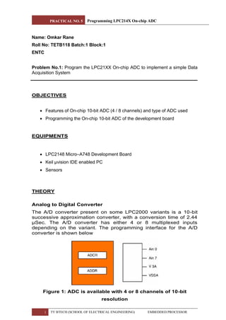
1. PRACTICAL NO. 5 Programming LPC214X On-chip ADC
1 TY BTECH (SCHOOL OF ELECTRICAL ENGINEERING) EMBEDDED PROCESSOR
Name: Omkar Rane
Roll No: TETB118 Batch:1 Block:1
ENTC
Problem No.1: Program the LPC21XX On-chip ADC to implement a simple Data
Acquisition System
OBJECTIVES
• Features of On-chip 10-bit ADC (4 / 8 channels) and type of ADC used
• Programming the On-chip 10-bit ADC of the development board
EQUIPMENTS
• LPC2148 Micro–A748 Development Board
• Keil µvision IDE enabled PC
• Sensors
THEORY
Analog to Digital Converter
The A/D converter present on some LPC2000 variants is a 10-bit
successive approximation converter, with a conversion time of 2.44
µSec. The A/D converter has either 4 or 8 multiplexed inputs
depending on the variant. The programming interface for the A/D
converter is shown below
Figure 1: ADC is available with 4 or 8 channels of 10-bit
resolution
2. PRACTICAL NO. 5 Programming LPC214X On-chip ADC
2 TY BTECH (SCHOOL OF ELECTRICAL ENGINEERING) EMBEDDED PROCESSOR
Features of ADC
• 2 internal ADC's - ADC0 (6 Channel), ADC1 (8 Channel)
• Type: 10-bit, Successive Approximation type,
• Supports burst mode (repeated conversion at 3-bit to 10-bit resolution)
• Supports simultaneous conversion on both ADC's
• Conversion time: 2.44 micro-seconds
• Start of Conversion by software control / on timer match /transition on a pin
• Range: 0 V – VREF (+3.3 V)
• Max. clock frequency is 4.5 MHz, (by programming ADC Control (ADxCON Register)
ADC Control Registers:
1. SEL: The bits from (0 to 7) are used to select the channel for ADC conversion. One bit is
allotted for each channel. For example setting the Bit-0 will make the ADC to sample AD0.1 for
conversion. And setting the bit -1 will make AD0.1; similarly setting bit-7 will do the conversion
for AD0.7. Important step is we have PINSEL according to the port we are using for example
PINSEL0 for PORT0 in PLC2148.
2. CLCKDIV: The bits from (8 to 15) are for Clock Divisor. Here the APB clock (ARM
Peripheral Bus clock) is divided by this value plus one to produce the clock required for the A/D
converter, which should be less than or equal to 4.5 MHz as we are using successive
approximation method in LPC2148.
3. BURST: The bit 16 is used for BURST conversion mode.
Setting 1: The ADC will do the conversion for all the channels that are selected in SEL bits.
Setting 0: Will disable the BURST conversion mode.
4. CLCKS: The bits from (17 to 19) three bits are used for selecting resolution and the number
of clocks for A/D conversion in burst mode as it is continuous A/D conversion mode.
5. PDN: The bit 21 is for selecting Power down Mode of ADC in LPC2148.
1. A/D is in PDN mode.
2. A/D is in operational mode
6. START: The bits from (24 to 26) are for START. When the BURST conversion mode is OFF
by setting 0, these START bits are useful for when to start the A/D conversion. The START is
used for edge controlled conversion also. That is when there is an input in CAP or MAT pin of
LPC2148 the A/D starts to convert.
7. EDGE: The 27th
bit is for EDGE is used only when the START bit contains 010-111. It starts
conversion when there is CAP or MAT input you can see above table for that.
Setting: 0 - On Falling Edge
1- On Rising Edge
3. PRACTICAL NO. 5 Programming LPC214X On-chip ADC
3 TY BTECH (SCHOOL OF ELECTRICAL ENGINEERING) EMBEDDED PROCESSOR
Configure ADC (AD0CR / AD1CR)
Observations:
Voltage Theoretical Values Practical
Values
ADC Hex
Values
1.0 V 1/1024=9.7656 mV 1021 V 013D
1.5 V 1.5/1024=1.4648 mV 1591 V 01EE
2.0 V 2/1024=1.9531 mV 2072 V 0283
2.5 V 2.5/1024=2.4414 mV 2587 V 0329
3.0 V 3/1024=2.587 mV 3106 V 03C4
3.1 V 3.1/1024=3.027 mV 3229 V 03EA
INTERFACING DETAILS / CONNECTIONS
4. PRACTICAL NO. 5 Programming LPC214X On-chip ADC
4 TY BTECH (SCHOOL OF ELECTRICAL ENGINEERING) EMBEDDED PROCESSOR
ALGORITHM / FLOWCHART
Steps for configuring the on-chip ADC
1. Configuring the ADC Power and ADC Port Pin
2. Configure ADC (AD0CR / AD1CR)
3. Reading the status of ADC
4. Reading the conversion results and displaying the Hex value on LCD display
PROGRAM CODE
adc_new.c file:
#include "lpc214x.h"
#include"stdio.h"
#include"UART.h"
#define ADC0 1<<24
#define ADC1 1<<26
#define ADC_ON 1<<21
#define ADC_Start 1<<24
#define ADC_Channel 0x03
#define ADC_Divider 0x03<<8
#define ADC_Burst 1<<16
#define ADC_CLKS 0x00<<17
void Display(int);
void adcdelay(unsigned int time)
{
unsigned int i,j;
for(i=0;i<time;i++)
{
for(j=0;j<10000;j++);
}
}
5. PRACTICAL NO. 5 Programming LPC214X On-chip ADC
5 TY BTECH (SCHOOL OF ELECTRICAL ENGINEERING) EMBEDDED PROCESSOR
void ADCInit(void)
{
int i;
i=PINSEL1;
i=(i& 0xF0FFFFFF);
PINSEL1=(i | (ADC0 | ADC1));
AD0CR=(ADC_Channel | ADC_Divider|ADC_Burst|ADC_CLKS);
i=AD0CR;
AD0CR=(i|ADC_ON);
}
unsigned int get_adc_voltage(unsigned int volt)
{
unsigned int volt_mv;
volt_mv=((volt*3300)/1024);
return volt_mv;
}
int main(void)
{
unsigned int ad0_data,ad1_data,voltage;
unsigned char * String="ADC Value(hex)";
UartInit(9600);
ADCInit();
//ADCInit();
printf("rn %s",String);
while(1)
{
if(AD0STAT & 0x03)
{
ad1_data=(AD0DR1 & 0x0000FFC0)>>6;
adcdelay(500);
voltage=get_adc_voltage(ad1_data);
printf("rnADC Voltage (mV)=%4d",voltage);
Display(ad1_data);
}
return 0;
}
}
6. PRACTICAL NO. 5 Programming LPC214X On-chip ADC
6 TY BTECH (SCHOOL OF ELECTRICAL ENGINEERING) EMBEDDED PROCESSOR
void Display(int v)
{
unsigned char Character[17]={"0123456789ABCDEF"};
unsigned char res[5]={"n"};
int i=0;
unsigned int DivValue=0x1000,BaseValue=16;
while(DivValue)
{
res[i]=Character[v/DivValue];
i++;
v%=DivValue;
DivValue/=BaseValue;
}
printf("rn ADC value in Hex = %s",res);
UART_PutChar('n');
}
Header File UART.h :
void UartInit(unsigned int);
int UART_PutChar(unsigned char);
UART.c file:
#include "lpc214x.h"
#include "stdio.h"
void UartInit(unsigned int baudrate) //setting the baud rate for
115200 baud
{
int i,FDiv;
i = PINSEL0; // read the value of the pins function
i = i & 0xFFFFFFF0; // modify the value
PINSEL0 = (i | 0x05); // set the functionality of the TxD and Rxd Pin
:01
7. PRACTICAL NO. 5 Programming LPC214X On-chip ADC
7 TY BTECH (SCHOOL OF ELECTRICAL ENGINEERING) EMBEDDED PROCESSOR
//set the baud rate
U0LCR = 0x83; // Line control
register :DLAB=1 ; 8 bits ; 1 stop bit ; no parity
FDiv = (15000000 / 16 ) / baudrate ; //
U0DLM = FDiv /256; //0x00;
U0DLL = FDiv %256; //0x97;
U0LCR = 0x03; // Line control
register :DLAB=0 ; 8 bits ; 1 stop bit ; no parity
U0TER = 0x80;
}
int UART_GetChar(void)
{
while(!(U0LSR & 0x1));
return(U0RBR);
}
int UART_PutChar(unsigned char Ch)
{
if (Ch == 'n') {
while (!(U0LSR & 0x20));
U0THR = 0x0D; /* output CR */
}
while(!(U0LSR & 0x20));
return( U0THR = Ch);
}
int fputc(int ch, FILE *f) {
return (UART_PutChar(ch));
}
struct __FILE { int handle; /* Add whatever you need here */ };
FILE __stdout;
8. PRACTICAL NO. 5 Programming LPC214X On-chip ADC
8 TY BTECH (SCHOOL OF ELECTRICAL ENGINEERING) EMBEDDED PROCESSOR
PROGRAM OUTPUT / RESULTS
Host Machine and Target Board
9. PRACTICAL NO. 5 Programming LPC214X On-chip ADC
9 TY BTECH (SCHOOL OF ELECTRICAL ENGINEERING) EMBEDDED PROCESSOR
10. PRACTICAL NO. 5 Programming LPC214X On-chip ADC
10 TY BTECH (SCHOOL OF ELECTRICAL ENGINEERING) EMBEDDED PROCESSOR
UART Readings On Host PC:
1.0 Volt
1.5 Volt
11. PRACTICAL NO. 5 Programming LPC214X On-chip ADC
11 TY BTECH (SCHOOL OF ELECTRICAL ENGINEERING) EMBEDDED PROCESSOR
2.0 Volt
2.5 Volt
12. PRACTICAL NO. 5 Programming LPC214X On-chip ADC
12 TY BTECH (SCHOOL OF ELECTRICAL ENGINEERING) EMBEDDED PROCESSOR
3.0 Volt
3.1 Volt
‘
13. PRACTICAL NO. 5 Programming LPC214X On-chip ADC
13 TY BTECH (SCHOOL OF ELECTRICAL ENGINEERING) EMBEDDED PROCESSOR
REFERENCES
1. Andrew Sloss, Dominic Symes, Chris Wright, “ARM System Developer’s
Guide – Designing and Optimizing System Software, ELSEVIER.
2. LPC 214x User manual (UM10139): www.nxp.com
3. ARM architecture reference manual: www.arm.com
4. Trevor Martin, “An Engineer’s Introduction to the LPC2100 series”, Hitex
(UK)
CONCLUSION
In this experiment we studied about various registers in ADC on chip peripheral
of LPC 2148 . We programmed them suitably to obtain respective results via
UART . AD0.1 was given voltage between 0-3.1 V and voltage readings
observed via UART on terminal screen. Theoretical and practical values almost
same.