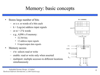
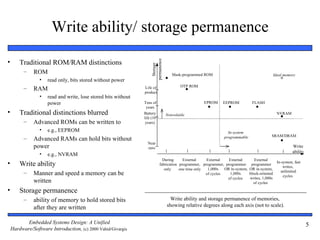
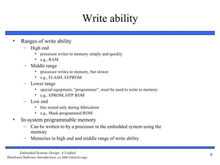
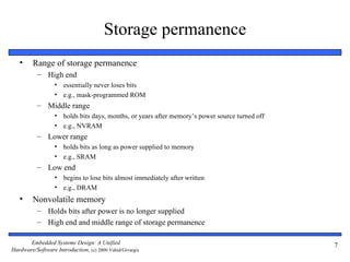
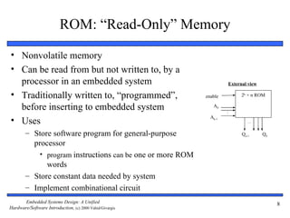
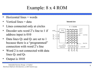
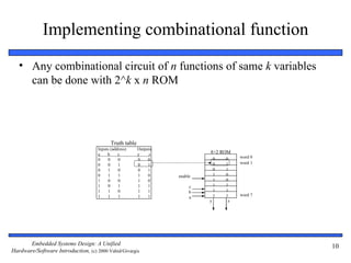
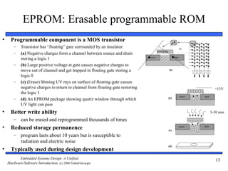
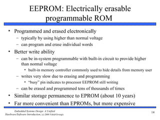
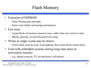
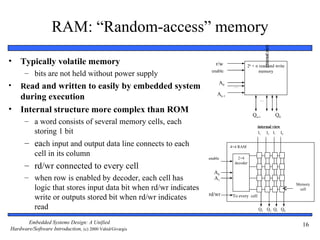
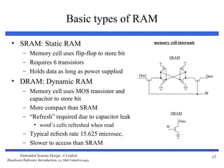
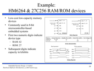
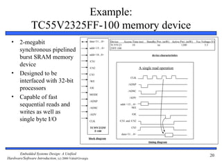
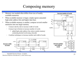
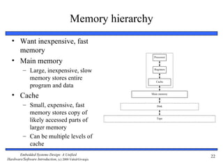
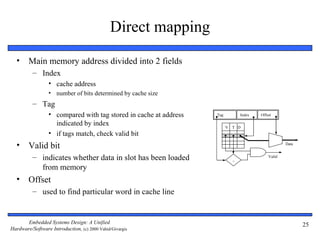
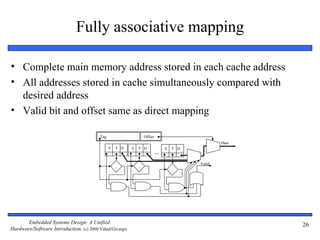
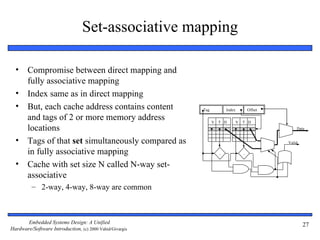
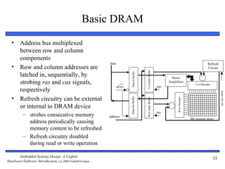
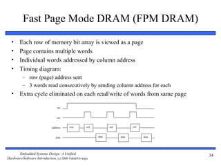
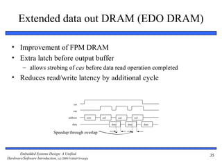
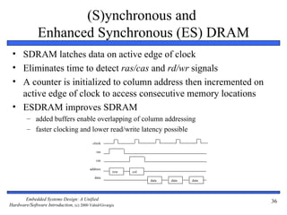
Embedded Systems Design: A Unified
  Hardware/Software Introduction


        Chapter 5 Memory


                                     1
Outline

  •     Memory Write Ability and Storage Permanence
  •     Common Memory Types
  •     Composing Memory
  •     Memory Hierarchy and Cache
  •     Advanced RAM


       Embedded Systems Design: A Unified                           2
Hardware/Software Introduction, (c) 2000 Vahid/Givargis
Introduction

   • Embedded system’s functionality aspects
           – Processing
                  • processors
                  • transformation of data
           – Storage
                  • memory
                  • retention of data
           – Communication
                  • buses
                  • transfer of data


       Embedded Systems Design: A Unified                         3
Hardware/Software Introduction, (c) 2000 Vahid/Givargis
Memory: basic concepts

  •     Stores large number of bits                                                   m × n memory

                                                                                                                     …
          –    m x n: m words of n bits each
          –    k = Log2(m) address input signals                           m words            …

          –    or m = 2^k words
          –    e.g., 4,096 x 8 memory:
                                                                                      n bits per word
                 • 32,768 bits


                                                                                                  memory external view
                 • 12 address input signals
                 • 8 input/output data signals
                                                                    r/w
                                                                                     2k × n read and write
  •     Memory access                                             enable                    memory

          – r/w: selects read or write                               A0
                                                                                …
          – enable: read or write only when asserted
                                                                    Ak-1
          – multiport: multiple accesses to different locations                            …

            simultaneously
                                                                                       Qn-1                              Q0

       Embedded Systems Design: A Unified                                                                                     4
Hardware/Software Introduction, (c) 2000 Vahid/Givargis
Write ability/ storage permanence

•       Traditional ROM/RAM distinctions


                                                                    permanence
                                                                      Storage
          –   ROM                                                                   Mask-programmed ROM                                     Ideal memory
                 •   read only, bits stored without power
                                                                                         OTP ROM
          –   RAM                                               Life of
                                                                product
                 •   read and write, lose stored bits without
                     power                                      Tens of                            EPROM      EEPROM            FLASH
                                                                  years
•       Traditional distinctions blurred                        Battery          Nonvolatile                                                   NVRAM
                                                                life (10
          –   Advanced ROMs can be written to                    years)
                 •   e.g., EEPROM                                                                                In-system
                                                                                                                                            SRAM/DRAM
          –   Advanced RAMs can hold bits without                                                              programmable
                                                                  Near
              power                                               zero                                                                                  Write
                                                                                                                                                        ability
                 •   e.g., NVRAM
                                                                             During      External    External    External         External
•       Write ability                                                      fabrication programmer, programmer, programmer       programmer
                                                                                                                                              In-system, fast
                                                                                                                                                  writes,
                                                                              only     one time only  1,000s   OR in-system,   OR in-system,
                                                                                                                                                unlimited
          –   Manner and speed a memory can be                                                       of cycles   1,000s        block-oriented
                                                                                                                                                  cycles
                                                                                                                of cycles      writes, 1,000s
              written                                                                                                            of cycles

•       Storage permanence
          –   ability of memory to hold stored bits                                Write ability and storage permanence of memories,
              after they are written                                             showing relative degrees along each axis (not to scale).


           Embedded Systems Design: A Unified                                                                                                                     5
    Hardware/Software Introduction, (c) 2000 Vahid/Givargis
Write ability
   •     Ranges of write ability
           – High end
                  • processor writes to memory simply and quickly
                  • e.g., RAM
           – Middle range
                  • processor writes to memory, but slower
                  • e.g., FLASH, EEPROM
           – Lower range
                  • special equipment, “programmer”, must be used to write to memory
                  • e.g., EPROM, OTP ROM
           – Low end
                  • bits stored only during fabrication
                  • e.g., Mask-programmed ROM
   •     In-system programmable memory
           – Can be written to by a processor in the embedded system using the
             memory
           – Memories in high end and middle range of write ability

       Embedded Systems Design: A Unified                                              6
Hardware/Software Introduction, (c) 2000 Vahid/Givargis
Storage permanence
   •     Range of storage permanence
           – High end
                  • essentially never loses bits
                  • e.g., mask-programmed ROM
           – Middle range
                  • holds bits days, months, or years after memory’s power source turned off
                  • e.g., NVRAM
           – Lower range
                  • holds bits as long as power supplied to memory
                  • e.g., SRAM
           – Low end
                  • begins to lose bits almost immediately after written
                  • e.g., DRAM
   •     Nonvolatile memory
           – Holds bits after power is no longer supplied
           – High end and middle range of storage permanence

       Embedded Systems Design: A Unified                                                      7
Hardware/Software Introduction, (c) 2000 Vahid/Givargis
ROM: “Read-Only” Memory
• Nonvolatile memory
• Can be read from but not written to, by a
  processor in an embedded system                                    External view

• Traditionally written to, “programmed”,                   enable         2k × n ROM

  before inserting to embedded system                          A0


                                                                     …
                                                              Ak-1
• Uses                                                                        …


        – Store software program for general-purpose                       Qn-1      Q0

          processor
            • program instructions can be one or more ROM
              words
        – Store constant data needed by system
        – Implement combinational circuit
       Embedded Systems Design: A Unified                                                 8
Hardware/Software Introduction, (c) 2000 Vahid/Givargis
Example: 8 x 4 ROM
• Horizontal lines = words
• Vertical lines = data                                                           Internal view


• Lines connected only at circles                                                    8 × 4 ROM
                                                                                                  word 0
• Decoder sets word 2’s line to 1 if                      enable      3×8
                                                                    decoder
                                                                                                  word 1
                                                                                                  word 2
  address input is 010                                    A0                                               word line
                                                          A1
• Data lines Q3 and Q1 are set to 1                       A2

  because there is a “programmed”                                                                          data line


  connection with word 2’s line                                    programmable
                                                                     connection                     wired-OR


• Word 2 is not connected with data                                                 Q3 Q2 Q1 Q0

  lines Q2 and Q0
• Output is 1010
       Embedded Systems Design: A Unified                                                                              9
Hardware/Software Introduction, (c) 2000 Vahid/Givargis
Implementing combinational function
   • Any combinational circuit of n functions of same k variables
     can be done with 2^k x n ROM


                                            Truth table
                                     Inputs (address)     Outputs
                                     a    b     c         y    z             8×2 ROM
                                                                                 0   0    word 0
                                     0    0     0         0    0
                                     0    0     1         0    1                 0   1    word 1
                                     0    1     0         0    1                 0   1
                                     0    1     1         1    0    enable       1   0
                                     1    0     0         1    0                 1   0
                                     1    0     1         1    1         c       1   1
                                     1    1     0         1    1         b       1   1
                                     1    1     1         1    1                 1   1    word 7
                                                                         a
                                                                             y        z


       Embedded Systems Design: A Unified                                                          10
Hardware/Software Introduction, (c) 2000 Vahid/Givargis
Mask-programmed ROM

      • Connections “programmed” at fabrication
              – set of masks
      • Lowest write ability
              – only once
      • Highest storage permanence
              – bits never change unless damaged
      • Typically used for final design of high-volume systems
              – spread out NRE cost for a low unit cost


       Embedded Systems Design: A Unified                        11
Hardware/Software Introduction, (c) 2000 Vahid/Givargis
OTP ROM: One-time programmable ROM
  • Connections “programmed” after manufacture by user
          –   user provides file of desired contents of ROM
          –   file input to machine called ROM programmer
          –   each programmable connection is a fuse
          –   ROM programmer blows fuses where connections should not exist
  • Very low write ability
          – typically written only once and requires ROM programmer device
  • Very high storage permanence
          – bits don’t change unless reconnected to programmer and more fuses
            blown
  • Commonly used in final products
          – cheaper, harder to inadvertently modify
       Embedded Systems Design: A Unified                                       12
Hardware/Software Introduction, (c) 2000 Vahid/Givargis
EPROM: Erasable programmable ROM
•     Programmable component is a MOS transistor
        –   Transistor has “floating” gate surrounded by an insulator                                                   0V
                                                                                          floating gate
        –   (a) Negative charges form a channel between source and drain
            storing a logic 1                                                    source                         drain


        –   (b) Large positive voltage at gate causes negative charges to
            move out of channel and get trapped in floating gate storing a                                (a)

            logic 0
        –   (c) (Erase) Shining UV rays on surface of floating-gate causes
            negative charges to return to channel from floating gate restoring                                                             +15V
            the logic 1
                                                                                                                        source   drain
        –   (d) An EPROM package showing quartz window through which                                      (b)

            UV light can pass
•     Better write ability                                                                                                               5-30 min
        – can be erased and reprogrammed thousands of times
•     Reduced storage permanence                                                                          (c)
                                                                                                                        source   drain


        – program lasts about 10 years but is susceptible to
          radiation and electric noise
                                                                                                          (d)
•     Typically used during design development
           Embedded Systems Design: A Unified                                                              .
                                                                                                                                            13
    Hardware/Software Introduction, (c) 2000 Vahid/Givargis
EEPROM: Electrically erasable
                         programmable ROM
  • Programmed and erased electronically
          – typically by using higher than normal voltage
          – can program and erase individual words
  • Better write ability
          – can be in-system programmable with built-in circuit to provide higher
            than normal voltage
                 • built-in memory controller commonly used to hide details from memory user
          – writes very slow due to erasing and programming
                 • “busy” pin indicates to processor EEPROM still writing
          – can be erased and programmed tens of thousands of times
  • Similar storage permanence to EPROM (about 10 years)
  • Far more convenient than EPROMs, but more expensive
       Embedded Systems Design: A Unified                                                  14
Hardware/Software Introduction, (c) 2000 Vahid/Givargis
Flash Memory

  • Extension of EEPROM
          – Same floating gate principle
          – Same write ability and storage permanence
  • Fast erase
          – Large blocks of memory erased at once, rather than one word at a time
          – Blocks typically several thousand bytes large
  • Writes to single words may be slower
          – Entire block must be read, word updated, then entire block written back
  • Used with embedded systems storing large data items in
    nonvolatile memory
          – e.g., digital cameras, TV set-top boxes, cell phones

       Embedded Systems Design: A Unified                                             15
Hardware/Software Introduction, (c) 2000 Vahid/Givargis
RAM: “Random-access” memory


                                                                                                external view
•   Typically volatile memory                                       r/w              2k × n read and write
      – bits are not held without power supply                   enable                     memory

                                                                     A0
•   Read and written to easily by embedded system                           …

                                                                    Ak-1
    during execution                                                                        …

•   Internal structure more complex than ROM                                            Qn-1                    Q0
      – a word consists of several memory cells, each
                                                                                            internal view
        storing 1 bit                                                                       I3 I2 I1 I0

      – each input and output data line connects to each                   4×4 RAM
           cell in its column                                   enable         2×4

      – rd/wr connected to every cell                                        decoder

                                                                   A0
      – when row is enabled by decoder, each cell has              A1
                                                                                                                     Memory
        logic that stores input data bit when rd/wr indicates                                                         cell
                                                                rd/wr
        write or outputs stored bit when rd/wr indicates                    To every cell

        read                                                                                Q3 Q2 Q1 Q0

       Embedded Systems Design: A Unified                                                                              16
Hardware/Software Introduction, (c) 2000 Vahid/Givargis
Basic types of RAM

  • SRAM: Static RAM                                              memory cell internals

          – Memory cell uses flip-flop to store bit
                                                                         SRAM
          – Requires 6 transistors
          – Holds data as long as power supplied
                                                          Data'                           Data
  • DRAM: Dynamic RAM
          – Memory cell uses MOS transistor and                                           W
            capacitor to store bit
          – More compact than SRAM
                                                                            DRAM
          – “Refresh” required due to capacitor leak
                                                                              Data
                 • word’s cells refreshed when read                     W

          – Typical refresh rate 15.625 microsec.
          – Slower to access than SRAM

       Embedded Systems Design: A Unified                                                     17
Hardware/Software Introduction, (c) 2000 Vahid/Givargis
Ram variations

  • PSRAM: Pseudo-static RAM
          – DRAM with built-in memory refresh controller
          – Popular low-cost high-density alternative to SRAM
  • NVRAM: Nonvolatile RAM
          – Holds data after external power removed
          – Battery-backed RAM
                 • SRAM with own permanently connected battery
                 • writes as fast as reads
                 • no limit on number of writes unlike nonvolatile ROM-based memory
          – SRAM with EEPROM or flash
                 • stores complete RAM contents on EEPROM or flash before power turned off


       Embedded Systems Design: A Unified                                                18
Hardware/Software Introduction, (c) 2000 Vahid/Givargis
Example:
        HM6264 & 27C256 RAM/ROM devices
  •     Low-cost low-capacity memory
        devices                                                11-13, 15-19        data<7…0>
                                                                                                              11-13, 15-19         data<7…0>
                                                                2,23,21,24,        addr<15...0>               27,26,2,23,21,       addr<15...0>
  •     Commonly used in 8-bit                                    25, 3-10
                                                                        22         /OE
                                                                                                                24,25, 3-10
                                                                                                                       22          /OE

        microcontroller-based                                           27         /WE                                   20        /CS

        embedded systems                                                20         /CS1

                                                                        26         CS2 HM6264                                             27C256
  •     First two numeric digits indicate                                                                block diagrams


        device type                                       Device
                                                          HM6264
                                                                 Access Time (ns)
                                                                     85-100
                                                                                          Standby Pwr. (mW)
                                                                                                 .01
                                                                                                                Active Pwr. (mW)
                                                                                                                        15
                                                                                                                                         Vcc Voltage (V)
                                                                                                                                                5
                                                          27C256        90                       .5                    100                      5
          – RAM: 62
                                                                                                device characteristics
          – ROM: 27                                               Read operation                                     Write operation

  •     Subsequent digits indicate                             data                                           data

        capacity in kilobits                                   addr
                                                                OE
                                                                                                              addr
                                                                                                              WE
                                                               /CS1                                           /CS1
                                                               CS2                                            CS2
                                                                                                   timing diagrams


       Embedded Systems Design: A Unified                                                                                                          19
Hardware/Software Introduction, (c) 2000 Vahid/Givargis
Example:
                TC55V2325FF-100 memory device
  •     2-megabit                                         data<31…0>      Device
                                                                          TC55V23
                                                                                   Access Time (ns)
                                                                                          10
                                                                                                      Standby Pwr. (mW)
                                                                                                               na
                                                                                                                           Active Pwr. (mW)
                                                                                                                                   1200
                                                                                                                                              Vcc Voltage (V)
                                                                                                                                                    3.3

        synchronous pipelined                             addr<15…0>      25FF-100

                                                          addr<10...0>
        burst SRAM memory                                                                                 device characteristics

                                                          /CS1
        device                                            /CS2                                  A single read operation
  •     Designed to be                                    CS3
                                                                                         CLK
        interfaced with 32-bit                            /WE
                                                                                       /ADSP
        processors                                        /OE
                                                                                       /ADSC

  •     Capable of fast
                                                          MODE
                                                                                        /ADV
                                                          /ADSP
        sequential reads and                              /ADSC
                                                                                 addr <15…0>
                                                                                         /WE
        writes as well as                                 /ADV                            /OE

        single byte I/O                                   CLK                   /CS1 and /CS2

                                                          TC55V2325F                     CS3
                                                             F-100
                                                                                  data<31…0>
                                                          block diagram
                                                                                                       timing diagram


       Embedded Systems Design: A Unified                                                                                                                20
Hardware/Software Introduction, (c) 2000 Vahid/Givargis
Composing memory
•      Memory size needed often differs from size of readily                                     Increase number of words
       available memories                                                                                  2m+1 × n ROM
•      When available memory is larger, simply ignore unneeded                                                          2m × n ROM

       high-order address bits and higher data lines                                A0
                                                                                            …                   …
                                                                                    Am-1
•      When available memory is smaller, compose several smaller                                  1×2                          …
                                                                                    Am           decoder
       memories into one larger memory
                                                                                                                        2m × n ROM
         –   Connect side-by-side to increase width of words
                                                                                  enable
         –   Connect top to bottom to increase number of words                                                  …
               • added high-order address line selects smaller memory                                                          …
                 containing desired word using a decoder
         –   Combine techniques to increase number and width of words
                                                                                                                               …
                                                                                                                        Qn-1       Q0
                                                   2m × 3n ROM
                     enable       2m × n ROM       2m × n ROM        2m × n ROM                                A

    Increase width                                                                         Increase number
                        A0                                                                   and width of
       of words               …                …                 …
                        Am                                                                      words
                                     …                    …            …                                       enable

                                  Q3n-1             Q2n-1                  Q0                                                      outputs


       Embedded Systems Design: A Unified                                                                                                    21
Hardware/Software Introduction, (c) 2000 Vahid/Givargis
Memory hierarchy
   • Want inexpensive, fast
     memory
                                                             Processor
   • Main memory
          – Large, inexpensive, slow                         Registers


            memory stores entire                              Cache
            program and data
   • Cache                                                Main memory


          – Small, expensive, fast                             Disk

            memory stores copy of
            likely accessed parts of                           Tape


            larger memory
          – Can be multiple levels of
            cache
       Embedded Systems Design: A Unified                                22
Hardware/Software Introduction, (c) 2000 Vahid/Givargis
Cache
  •     Usually designed with SRAM
          – faster but more expensive than DRAM
  •     Usually on same chip as processor
          – space limited, so much smaller than off-chip main memory
          – faster access ( 1 cycle vs. several cycles for main memory)
  •     Cache operation:
          – Request for main memory access (read or write)
          – First, check cache for copy
                 • cache hit
                         – copy is in cache, quick access
                 • cache miss
                         – copy not in cache, read address and possibly its neighbors into cache
  •     Several cache design choices
          – cache mapping, replacement policies, and write techniques
       Embedded Systems Design: A Unified                                                          23
Hardware/Software Introduction, (c) 2000 Vahid/Givargis
Cache mapping

  • Far fewer number of available cache addresses
  • Are address’ contents in cache?
  • Cache mapping used to assign main memory address to cache
    address and determine hit or miss
  • Three basic techniques:
          – Direct mapping
          – Fully associative mapping
          – Set-associative mapping
  • Caches partitioned into indivisible blocks or lines of adjacent
    memory addresses
          – usually 4 or 8 addresses per line

       Embedded Systems Design: A Unified                             24
Hardware/Software Introduction, (c) 2000 Vahid/Givargis
Direct mapping
  •     Main memory address divided into 2 fields
          – Index
                 • cache address
                 • number of bits determined by cache size
          – Tag
                 • compared with tag stored in cache at address   Tag           Index   Offset

                   indicated by index                                   V   T D
                 • if tags match, check valid bit
  •     Valid bit                                                                                   Data


          – indicates whether data in slot has been loaded                  =
                                                                                            Valid

            from memory
  •     Offset
          – used to find particular word in cache line


       Embedded Systems Design: A Unified                                                                  25
Hardware/Software Introduction, (c) 2000 Vahid/Givargis
Fully associative mapping

• Complete main memory address stored in each cache address
• All addresses stored in cache simultaneously compared with
  desired address
• Valid bit and offset same as direct mapping

                                          Tag                     Offset
                                                                                                 Data
                                                V   T D   V   T D              V   T D
                                                                           …

                                                                                         Valid
                                                    =         =
                                                                                   =


       Embedded Systems Design: A Unified                                                               26
Hardware/Software Introduction, (c) 2000 Vahid/Givargis
Set-associative mapping

  •     Compromise between direct mapping and
        fully associative mapping
  •     Index same as in direct mapping
  •     But, each cache address contains content          Tag           Index           Offset

        and tags of 2 or more memory address                    V   T D         V   T D
        locations                                                                                    Data


  •     Tags of that set simultaneously compared as                                              Valid

        in fully associative mapping                                =               =

  •     Cache with set size N called N-way set-
        associative
         – 2-way, 4-way, 8-way are common


       Embedded Systems Design: A Unified                                                                27
Hardware/Software Introduction, (c) 2000 Vahid/Givargis
Cache-replacement policy

  • Technique for choosing which block to replace
          – when fully associative cache is full
          – when set-associative cache’s line is full
  • Direct mapped cache has no choice
  • Random
          – replace block chosen at random
  • LRU: least-recently used
          – replace block not accessed for longest time
  • FIFO: first-in-first-out
          – push block onto queue when accessed
          – choose block to replace by popping queue

       Embedded Systems Design: A Unified                 28
Hardware/Software Introduction, (c) 2000 Vahid/Givargis
Cache write techniques

  • When written, data cache must update main memory
  • Write-through
          –    write to main memory whenever cache is written to
          –    easiest to implement
          –    processor must wait for slower main memory write
          –    potential for unnecessary writes
  • Write-back
          – main memory only written when “dirty” block replaced
          – extra dirty bit for each block set when cache block written to
          – reduces number of slow main memory writes


       Embedded Systems Design: A Unified                                    29
Hardware/Software Introduction, (c) 2000 Vahid/Givargis
Cache impact on system performance
 • Most important parameters in terms of performance:
         – Total size of cache
                • total number of data bytes cache can hold
                • tag, valid and other house keeping bits not included in total
         – Degree of associativity
         – Data block size
 • Larger caches achieve lower miss rates but higher access cost
         – e.g.,
                • 2 Kbyte cache: miss rate = 15%, hit cost = 2 cycles, miss cost = 20 cycles
                        – avg. cost of memory access = (0.85 * 2) + (0.15 * 20) = 4.7 cycles
                • 4 Kbyte cache: miss rate = 6.5%, hit cost = 3 cycles, miss cost will not change
                        – avg. cost of memory access = (0.935 * 3) + (0.065 * 20) = 4.105 cycles   (improvement)
                • 8 Kbyte cache: miss rate = 5.565%, hit cost = 4 cycles, miss cost will not change
                        – avg. cost of memory access = (0.94435 * 4) + (0.05565 * 20) = 4.8904 cycles   (worse)

       Embedded Systems Design: A Unified                                                                         30
Hardware/Software Introduction, (c) 2000 Vahid/Givargis
Cache performance trade-offs

  • Improving cache hit rate without increasing size
          – Increase line size
          – Change set-associativity

                                          0.16

                                          0.14

                                          0.12
                           % cache miss


                                           0.1                                                                    1 way
                                                                                                                  2 way
                                          0.08
                                                                                                                  4 way
                                          0.06                                                                    8 way

                                          0.04

                                          0.02

                                            0
                                                                                                          cache size
                                                 1 Kb   2 Kb   4 Kb   8 Kb   16 Kb 32 Kb   64 Kb 128 Kb


       Embedded Systems Design: A Unified                                                                                 31
Hardware/Software Introduction, (c) 2000 Vahid/Givargis
Advanced RAM

      • DRAMs commonly used as main memory in processor
        based embedded systems
              – high capacity, low cost
      • Many variations of DRAMs proposed
              – need to keep pace with processor speeds
              – FPM DRAM: fast page mode DRAM
              – EDO DRAM: extended data out DRAM
              – SDRAM/ESDRAM: synchronous and enhanced synchronous
                DRAM
              – RDRAM: rambus DRAM


       Embedded Systems Design: A Unified                            32
Hardware/Software Introduction, (c) 2000 Vahid/Givargis
Basic DRAM
  •     Address bus multiplexed
        between row and column
        components
                                                          data                                                                                      Refresh
  •     Row and column addresses are                                                                                                                Circuit


                                                                                           Col Addr. Buffer
        latched in, sequentially, by


                                                                          Data In Buffer
                                                                                                                     Sense
        strobing ras and cas signals,                                                                               Amplifiers
                                                                                                                                           Col Decoder
                                                                 rd/wr                                        cas
        respectively


                                                                                                                                                              cas, ras, clock
  •     Refresh circuitry can be external


                                                                         Data Out Buffer


                                                                                                                          Row Decoder
                                                                                           Row Addr. Buffer
        or internal to DRAM device
                                                                                                              ras
          – strobes consecutive memory                    address
                                                                                                                                        Bit storage array
            address periodically causing
            memory content to be refreshed
          – Refresh circuitry disabled
            during read or write operation

       Embedded Systems Design: A Unified                                                                                                                33
Hardware/Software Introduction, (c) 2000 Vahid/Givargis
Fast Page Mode DRAM (FPM DRAM)
  •     Each row of memory bit array is viewed as a page
  •     Page contains multiple words
  •     Individual words addressed by column address
  •     Timing diagram:
          – row (page) address sent
          – 3 words read consecutively by sending column address for each
  •     Extra cycle eliminated on each read/write of words from same page

                                  ras


                                  cas


                              address     row         col          col          col


                                 data                       data         data         data


       Embedded Systems Design: A Unified                                                    34
Hardware/Software Introduction, (c) 2000 Vahid/Givargis
Extended data out DRAM (EDO DRAM)

   • Improvement of FPM DRAM
   • Extra latch before output buffer
          – allows strobing of cas before data read operation completed
   • Reduces read/write latency by additional cycle


                                             ras

                                             cas

                                         address      row   col          col          col

                                            data                  data         data         data


                               Speedup through overlap


       Embedded Systems Design: A Unified                                                          35
Hardware/Software Introduction, (c) 2000 Vahid/Givargis
(S)ynchronous and
              Enhanced Synchronous (ES) DRAM
 • SDRAM latches data on active edge of clock
 • Eliminates time to detect ras/cas and rd/wr signals
 • A counter is initialized to column address then incremented on
   active edge of clock to access consecutive memory locations
 • ESDRAM improves SDRAM
         – added buffers enable overlapping of column addressing
         – faster clocking and lower read/write latency possible
                                           clock

                                              ras

                                              cas

                                          address
                                                      row   col
                                             data
                                                                  data   data   data


       Embedded Systems Design: A Unified                                              36
Hardware/Software Introduction, (c) 2000 Vahid/Givargis
Rambus DRAM (RDRAM)

   • More of a bus interface architecture than DRAM
     architecture
   • Data is latched on both rising and falling edge of
     clock
   • Broken into 4 banks each with own row decoder
           – can have 4 pages open at a time
   • Capable of very high throughput


       Embedded Systems Design: A Unified                 37
Hardware/Software Introduction, (c) 2000 Vahid/Givargis
DRAM integration problem

  • SRAM easily integrated on same chip as processor
  • DRAM more difficult
          – Different chip making process between DRAM and
            conventional logic
          – Goal of conventional logic (IC) designers:
                 • minimize parasitic capacitance to reduce signal propagation delays
                   and power consumption
          – Goal of DRAM designers:
                 • create capacitor cells to retain stored information
          – Integration processes beginning to appear

       Embedded Systems Design: A Unified                                               38
Hardware/Software Introduction, (c) 2000 Vahid/Givargis
Memory Management Unit (MMU)

     • Duties of MMU
             – Handles DRAM refresh, bus interface and arbitration
             – Takes care of memory sharing among multiple
               processors
             – Translates logic memory addresses from processor to
               physical memory addresses of DRAM
     • Modern CPUs often come with MMU built-in
     • Single-purpose processors can be used


       Embedded Systems Design: A Unified                            39
Hardware/Software Introduction, (c) 2000 Vahid/Givargis

Ch5

  • 1.
    Embedded Systems Design:A Unified Hardware/Software Introduction Chapter 5 Memory 1
  • 2.
    Outline • Memory Write Ability and Storage Permanence • Common Memory Types • Composing Memory • Memory Hierarchy and Cache • Advanced RAM Embedded Systems Design: A Unified 2 Hardware/Software Introduction, (c) 2000 Vahid/Givargis
  • 3.
    Introduction • Embedded system’s functionality aspects – Processing • processors • transformation of data – Storage • memory • retention of data – Communication • buses • transfer of data Embedded Systems Design: A Unified 3 Hardware/Software Introduction, (c) 2000 Vahid/Givargis
  • 4.
    Memory: basic concepts • Stores large number of bits m × n memory … – m x n: m words of n bits each – k = Log2(m) address input signals m words … – or m = 2^k words – e.g., 4,096 x 8 memory: n bits per word • 32,768 bits memory external view • 12 address input signals • 8 input/output data signals r/w 2k × n read and write • Memory access enable memory – r/w: selects read or write A0 … – enable: read or write only when asserted Ak-1 – multiport: multiple accesses to different locations … simultaneously Qn-1 Q0 Embedded Systems Design: A Unified 4 Hardware/Software Introduction, (c) 2000 Vahid/Givargis
  • 5.
    Write ability/ storagepermanence • Traditional ROM/RAM distinctions permanence Storage – ROM Mask-programmed ROM Ideal memory • read only, bits stored without power OTP ROM – RAM Life of product • read and write, lose stored bits without power Tens of EPROM EEPROM FLASH years • Traditional distinctions blurred Battery Nonvolatile NVRAM life (10 – Advanced ROMs can be written to years) • e.g., EEPROM In-system SRAM/DRAM – Advanced RAMs can hold bits without programmable Near power zero Write ability • e.g., NVRAM During External External External External • Write ability fabrication programmer, programmer, programmer programmer In-system, fast writes, only one time only 1,000s OR in-system, OR in-system, unlimited – Manner and speed a memory can be of cycles 1,000s block-oriented cycles of cycles writes, 1,000s written of cycles • Storage permanence – ability of memory to hold stored bits Write ability and storage permanence of memories, after they are written showing relative degrees along each axis (not to scale). Embedded Systems Design: A Unified 5 Hardware/Software Introduction, (c) 2000 Vahid/Givargis
  • 6.
    Write ability • Ranges of write ability – High end • processor writes to memory simply and quickly • e.g., RAM – Middle range • processor writes to memory, but slower • e.g., FLASH, EEPROM – Lower range • special equipment, “programmer”, must be used to write to memory • e.g., EPROM, OTP ROM – Low end • bits stored only during fabrication • e.g., Mask-programmed ROM • In-system programmable memory – Can be written to by a processor in the embedded system using the memory – Memories in high end and middle range of write ability Embedded Systems Design: A Unified 6 Hardware/Software Introduction, (c) 2000 Vahid/Givargis
  • 7.
    Storage permanence • Range of storage permanence – High end • essentially never loses bits • e.g., mask-programmed ROM – Middle range • holds bits days, months, or years after memory’s power source turned off • e.g., NVRAM – Lower range • holds bits as long as power supplied to memory • e.g., SRAM – Low end • begins to lose bits almost immediately after written • e.g., DRAM • Nonvolatile memory – Holds bits after power is no longer supplied – High end and middle range of storage permanence Embedded Systems Design: A Unified 7 Hardware/Software Introduction, (c) 2000 Vahid/Givargis
  • 8.
    ROM: “Read-Only” Memory •Nonvolatile memory • Can be read from but not written to, by a processor in an embedded system External view • Traditionally written to, “programmed”, enable 2k × n ROM before inserting to embedded system A0 … Ak-1 • Uses … – Store software program for general-purpose Qn-1 Q0 processor • program instructions can be one or more ROM words – Store constant data needed by system – Implement combinational circuit Embedded Systems Design: A Unified 8 Hardware/Software Introduction, (c) 2000 Vahid/Givargis
  • 9.
    Example: 8 x4 ROM • Horizontal lines = words • Vertical lines = data Internal view • Lines connected only at circles 8 × 4 ROM word 0 • Decoder sets word 2’s line to 1 if enable 3×8 decoder word 1 word 2 address input is 010 A0 word line A1 • Data lines Q3 and Q1 are set to 1 A2 because there is a “programmed” data line connection with word 2’s line programmable connection wired-OR • Word 2 is not connected with data Q3 Q2 Q1 Q0 lines Q2 and Q0 • Output is 1010 Embedded Systems Design: A Unified 9 Hardware/Software Introduction, (c) 2000 Vahid/Givargis
  • 10.
    Implementing combinational function • Any combinational circuit of n functions of same k variables can be done with 2^k x n ROM Truth table Inputs (address) Outputs a b c y z 8×2 ROM 0 0 word 0 0 0 0 0 0 0 0 1 0 1 0 1 word 1 0 1 0 0 1 0 1 0 1 1 1 0 enable 1 0 1 0 0 1 0 1 0 1 0 1 1 1 c 1 1 1 1 0 1 1 b 1 1 1 1 1 1 1 1 1 word 7 a y z Embedded Systems Design: A Unified 10 Hardware/Software Introduction, (c) 2000 Vahid/Givargis
  • 11.
    Mask-programmed ROM • Connections “programmed” at fabrication – set of masks • Lowest write ability – only once • Highest storage permanence – bits never change unless damaged • Typically used for final design of high-volume systems – spread out NRE cost for a low unit cost Embedded Systems Design: A Unified 11 Hardware/Software Introduction, (c) 2000 Vahid/Givargis
  • 12.
    OTP ROM: One-timeprogrammable ROM • Connections “programmed” after manufacture by user – user provides file of desired contents of ROM – file input to machine called ROM programmer – each programmable connection is a fuse – ROM programmer blows fuses where connections should not exist • Very low write ability – typically written only once and requires ROM programmer device • Very high storage permanence – bits don’t change unless reconnected to programmer and more fuses blown • Commonly used in final products – cheaper, harder to inadvertently modify Embedded Systems Design: A Unified 12 Hardware/Software Introduction, (c) 2000 Vahid/Givargis
  • 13.
    EPROM: Erasable programmableROM • Programmable component is a MOS transistor – Transistor has “floating” gate surrounded by an insulator 0V floating gate – (a) Negative charges form a channel between source and drain storing a logic 1 source drain – (b) Large positive voltage at gate causes negative charges to move out of channel and get trapped in floating gate storing a (a) logic 0 – (c) (Erase) Shining UV rays on surface of floating-gate causes negative charges to return to channel from floating gate restoring +15V the logic 1 source drain – (d) An EPROM package showing quartz window through which (b) UV light can pass • Better write ability 5-30 min – can be erased and reprogrammed thousands of times • Reduced storage permanence (c) source drain – program lasts about 10 years but is susceptible to radiation and electric noise (d) • Typically used during design development Embedded Systems Design: A Unified . 13 Hardware/Software Introduction, (c) 2000 Vahid/Givargis
  • 14.
    EEPROM: Electrically erasable programmable ROM • Programmed and erased electronically – typically by using higher than normal voltage – can program and erase individual words • Better write ability – can be in-system programmable with built-in circuit to provide higher than normal voltage • built-in memory controller commonly used to hide details from memory user – writes very slow due to erasing and programming • “busy” pin indicates to processor EEPROM still writing – can be erased and programmed tens of thousands of times • Similar storage permanence to EPROM (about 10 years) • Far more convenient than EPROMs, but more expensive Embedded Systems Design: A Unified 14 Hardware/Software Introduction, (c) 2000 Vahid/Givargis
  • 15.
    Flash Memory • Extension of EEPROM – Same floating gate principle – Same write ability and storage permanence • Fast erase – Large blocks of memory erased at once, rather than one word at a time – Blocks typically several thousand bytes large • Writes to single words may be slower – Entire block must be read, word updated, then entire block written back • Used with embedded systems storing large data items in nonvolatile memory – e.g., digital cameras, TV set-top boxes, cell phones Embedded Systems Design: A Unified 15 Hardware/Software Introduction, (c) 2000 Vahid/Givargis
  • 16.
    RAM: “Random-access” memory external view • Typically volatile memory r/w 2k × n read and write – bits are not held without power supply enable memory A0 • Read and written to easily by embedded system … Ak-1 during execution … • Internal structure more complex than ROM Qn-1 Q0 – a word consists of several memory cells, each internal view storing 1 bit I3 I2 I1 I0 – each input and output data line connects to each 4×4 RAM cell in its column enable 2×4 – rd/wr connected to every cell decoder A0 – when row is enabled by decoder, each cell has A1 Memory logic that stores input data bit when rd/wr indicates cell rd/wr write or outputs stored bit when rd/wr indicates To every cell read Q3 Q2 Q1 Q0 Embedded Systems Design: A Unified 16 Hardware/Software Introduction, (c) 2000 Vahid/Givargis
  • 17.
    Basic types ofRAM • SRAM: Static RAM memory cell internals – Memory cell uses flip-flop to store bit SRAM – Requires 6 transistors – Holds data as long as power supplied Data' Data • DRAM: Dynamic RAM – Memory cell uses MOS transistor and W capacitor to store bit – More compact than SRAM DRAM – “Refresh” required due to capacitor leak Data • word’s cells refreshed when read W – Typical refresh rate 15.625 microsec. – Slower to access than SRAM Embedded Systems Design: A Unified 17 Hardware/Software Introduction, (c) 2000 Vahid/Givargis
  • 18.
    Ram variations • PSRAM: Pseudo-static RAM – DRAM with built-in memory refresh controller – Popular low-cost high-density alternative to SRAM • NVRAM: Nonvolatile RAM – Holds data after external power removed – Battery-backed RAM • SRAM with own permanently connected battery • writes as fast as reads • no limit on number of writes unlike nonvolatile ROM-based memory – SRAM with EEPROM or flash • stores complete RAM contents on EEPROM or flash before power turned off Embedded Systems Design: A Unified 18 Hardware/Software Introduction, (c) 2000 Vahid/Givargis
  • 19.
    Example: HM6264 & 27C256 RAM/ROM devices • Low-cost low-capacity memory devices 11-13, 15-19 data<7…0> 11-13, 15-19 data<7…0> 2,23,21,24, addr<15...0> 27,26,2,23,21, addr<15...0> • Commonly used in 8-bit 25, 3-10 22 /OE 24,25, 3-10 22 /OE microcontroller-based 27 /WE 20 /CS embedded systems 20 /CS1 26 CS2 HM6264 27C256 • First two numeric digits indicate block diagrams device type Device HM6264 Access Time (ns) 85-100 Standby Pwr. (mW) .01 Active Pwr. (mW) 15 Vcc Voltage (V) 5 27C256 90 .5 100 5 – RAM: 62 device characteristics – ROM: 27 Read operation Write operation • Subsequent digits indicate data data capacity in kilobits addr OE addr WE /CS1 /CS1 CS2 CS2 timing diagrams Embedded Systems Design: A Unified 19 Hardware/Software Introduction, (c) 2000 Vahid/Givargis
  • 20.
    Example: TC55V2325FF-100 memory device • 2-megabit data<31…0> Device TC55V23 Access Time (ns) 10 Standby Pwr. (mW) na Active Pwr. (mW) 1200 Vcc Voltage (V) 3.3 synchronous pipelined addr<15…0> 25FF-100 addr<10...0> burst SRAM memory device characteristics /CS1 device /CS2 A single read operation • Designed to be CS3 CLK interfaced with 32-bit /WE /ADSP processors /OE /ADSC • Capable of fast MODE /ADV /ADSP sequential reads and /ADSC addr <15…0> /WE writes as well as /ADV /OE single byte I/O CLK /CS1 and /CS2 TC55V2325F CS3 F-100 data<31…0> block diagram timing diagram Embedded Systems Design: A Unified 20 Hardware/Software Introduction, (c) 2000 Vahid/Givargis
  • 21.
    Composing memory • Memory size needed often differs from size of readily Increase number of words available memories 2m+1 × n ROM • When available memory is larger, simply ignore unneeded 2m × n ROM high-order address bits and higher data lines A0 … … Am-1 • When available memory is smaller, compose several smaller 1×2 … Am decoder memories into one larger memory 2m × n ROM – Connect side-by-side to increase width of words enable – Connect top to bottom to increase number of words … • added high-order address line selects smaller memory … containing desired word using a decoder – Combine techniques to increase number and width of words … Qn-1 Q0 2m × 3n ROM enable 2m × n ROM 2m × n ROM 2m × n ROM A Increase width Increase number A0 and width of of words … … … Am words … … … enable Q3n-1 Q2n-1 Q0 outputs Embedded Systems Design: A Unified 21 Hardware/Software Introduction, (c) 2000 Vahid/Givargis
  • 22.
    Memory hierarchy • Want inexpensive, fast memory Processor • Main memory – Large, inexpensive, slow Registers memory stores entire Cache program and data • Cache Main memory – Small, expensive, fast Disk memory stores copy of likely accessed parts of Tape larger memory – Can be multiple levels of cache Embedded Systems Design: A Unified 22 Hardware/Software Introduction, (c) 2000 Vahid/Givargis
  • 23.
    Cache • Usually designed with SRAM – faster but more expensive than DRAM • Usually on same chip as processor – space limited, so much smaller than off-chip main memory – faster access ( 1 cycle vs. several cycles for main memory) • Cache operation: – Request for main memory access (read or write) – First, check cache for copy • cache hit – copy is in cache, quick access • cache miss – copy not in cache, read address and possibly its neighbors into cache • Several cache design choices – cache mapping, replacement policies, and write techniques Embedded Systems Design: A Unified 23 Hardware/Software Introduction, (c) 2000 Vahid/Givargis
  • 24.
    Cache mapping • Far fewer number of available cache addresses • Are address’ contents in cache? • Cache mapping used to assign main memory address to cache address and determine hit or miss • Three basic techniques: – Direct mapping – Fully associative mapping – Set-associative mapping • Caches partitioned into indivisible blocks or lines of adjacent memory addresses – usually 4 or 8 addresses per line Embedded Systems Design: A Unified 24 Hardware/Software Introduction, (c) 2000 Vahid/Givargis
  • 25.
    Direct mapping • Main memory address divided into 2 fields – Index • cache address • number of bits determined by cache size – Tag • compared with tag stored in cache at address Tag Index Offset indicated by index V T D • if tags match, check valid bit • Valid bit Data – indicates whether data in slot has been loaded = Valid from memory • Offset – used to find particular word in cache line Embedded Systems Design: A Unified 25 Hardware/Software Introduction, (c) 2000 Vahid/Givargis
  • 26.
    Fully associative mapping •Complete main memory address stored in each cache address • All addresses stored in cache simultaneously compared with desired address • Valid bit and offset same as direct mapping Tag Offset Data V T D V T D V T D … Valid = = = Embedded Systems Design: A Unified 26 Hardware/Software Introduction, (c) 2000 Vahid/Givargis
  • 27.
    Set-associative mapping • Compromise between direct mapping and fully associative mapping • Index same as in direct mapping • But, each cache address contains content Tag Index Offset and tags of 2 or more memory address V T D V T D locations Data • Tags of that set simultaneously compared as Valid in fully associative mapping = = • Cache with set size N called N-way set- associative – 2-way, 4-way, 8-way are common Embedded Systems Design: A Unified 27 Hardware/Software Introduction, (c) 2000 Vahid/Givargis
  • 28.
    Cache-replacement policy • Technique for choosing which block to replace – when fully associative cache is full – when set-associative cache’s line is full • Direct mapped cache has no choice • Random – replace block chosen at random • LRU: least-recently used – replace block not accessed for longest time • FIFO: first-in-first-out – push block onto queue when accessed – choose block to replace by popping queue Embedded Systems Design: A Unified 28 Hardware/Software Introduction, (c) 2000 Vahid/Givargis
  • 29.
    Cache write techniques • When written, data cache must update main memory • Write-through – write to main memory whenever cache is written to – easiest to implement – processor must wait for slower main memory write – potential for unnecessary writes • Write-back – main memory only written when “dirty” block replaced – extra dirty bit for each block set when cache block written to – reduces number of slow main memory writes Embedded Systems Design: A Unified 29 Hardware/Software Introduction, (c) 2000 Vahid/Givargis
  • 30.
    Cache impact onsystem performance • Most important parameters in terms of performance: – Total size of cache • total number of data bytes cache can hold • tag, valid and other house keeping bits not included in total – Degree of associativity – Data block size • Larger caches achieve lower miss rates but higher access cost – e.g., • 2 Kbyte cache: miss rate = 15%, hit cost = 2 cycles, miss cost = 20 cycles – avg. cost of memory access = (0.85 * 2) + (0.15 * 20) = 4.7 cycles • 4 Kbyte cache: miss rate = 6.5%, hit cost = 3 cycles, miss cost will not change – avg. cost of memory access = (0.935 * 3) + (0.065 * 20) = 4.105 cycles (improvement) • 8 Kbyte cache: miss rate = 5.565%, hit cost = 4 cycles, miss cost will not change – avg. cost of memory access = (0.94435 * 4) + (0.05565 * 20) = 4.8904 cycles (worse) Embedded Systems Design: A Unified 30 Hardware/Software Introduction, (c) 2000 Vahid/Givargis
  • 31.
    Cache performance trade-offs • Improving cache hit rate without increasing size – Increase line size – Change set-associativity 0.16 0.14 0.12 % cache miss 0.1 1 way 2 way 0.08 4 way 0.06 8 way 0.04 0.02 0 cache size 1 Kb 2 Kb 4 Kb 8 Kb 16 Kb 32 Kb 64 Kb 128 Kb Embedded Systems Design: A Unified 31 Hardware/Software Introduction, (c) 2000 Vahid/Givargis
  • 32.
    Advanced RAM • DRAMs commonly used as main memory in processor based embedded systems – high capacity, low cost • Many variations of DRAMs proposed – need to keep pace with processor speeds – FPM DRAM: fast page mode DRAM – EDO DRAM: extended data out DRAM – SDRAM/ESDRAM: synchronous and enhanced synchronous DRAM – RDRAM: rambus DRAM Embedded Systems Design: A Unified 32 Hardware/Software Introduction, (c) 2000 Vahid/Givargis
  • 33.
    Basic DRAM • Address bus multiplexed between row and column components data Refresh • Row and column addresses are Circuit Col Addr. Buffer latched in, sequentially, by Data In Buffer Sense strobing ras and cas signals, Amplifiers Col Decoder rd/wr cas respectively cas, ras, clock • Refresh circuitry can be external Data Out Buffer Row Decoder Row Addr. Buffer or internal to DRAM device ras – strobes consecutive memory address Bit storage array address periodically causing memory content to be refreshed – Refresh circuitry disabled during read or write operation Embedded Systems Design: A Unified 33 Hardware/Software Introduction, (c) 2000 Vahid/Givargis
  • 34.
    Fast Page ModeDRAM (FPM DRAM) • Each row of memory bit array is viewed as a page • Page contains multiple words • Individual words addressed by column address • Timing diagram: – row (page) address sent – 3 words read consecutively by sending column address for each • Extra cycle eliminated on each read/write of words from same page ras cas address row col col col data data data data Embedded Systems Design: A Unified 34 Hardware/Software Introduction, (c) 2000 Vahid/Givargis
  • 35.
    Extended data outDRAM (EDO DRAM) • Improvement of FPM DRAM • Extra latch before output buffer – allows strobing of cas before data read operation completed • Reduces read/write latency by additional cycle ras cas address row col col col data data data data Speedup through overlap Embedded Systems Design: A Unified 35 Hardware/Software Introduction, (c) 2000 Vahid/Givargis
  • 36.
    (S)ynchronous and Enhanced Synchronous (ES) DRAM • SDRAM latches data on active edge of clock • Eliminates time to detect ras/cas and rd/wr signals • A counter is initialized to column address then incremented on active edge of clock to access consecutive memory locations • ESDRAM improves SDRAM – added buffers enable overlapping of column addressing – faster clocking and lower read/write latency possible clock ras cas address row col data data data data Embedded Systems Design: A Unified 36 Hardware/Software Introduction, (c) 2000 Vahid/Givargis
  • 37.
    Rambus DRAM (RDRAM) • More of a bus interface architecture than DRAM architecture • Data is latched on both rising and falling edge of clock • Broken into 4 banks each with own row decoder – can have 4 pages open at a time • Capable of very high throughput Embedded Systems Design: A Unified 37 Hardware/Software Introduction, (c) 2000 Vahid/Givargis
  • 38.
    DRAM integration problem • SRAM easily integrated on same chip as processor • DRAM more difficult – Different chip making process between DRAM and conventional logic – Goal of conventional logic (IC) designers: • minimize parasitic capacitance to reduce signal propagation delays and power consumption – Goal of DRAM designers: • create capacitor cells to retain stored information – Integration processes beginning to appear Embedded Systems Design: A Unified 38 Hardware/Software Introduction, (c) 2000 Vahid/Givargis
  • 39.
    Memory Management Unit(MMU) • Duties of MMU – Handles DRAM refresh, bus interface and arbitration – Takes care of memory sharing among multiple processors – Translates logic memory addresses from processor to physical memory addresses of DRAM • Modern CPUs often come with MMU built-in • Single-purpose processors can be used Embedded Systems Design: A Unified 39 Hardware/Software Introduction, (c) 2000 Vahid/Givargis