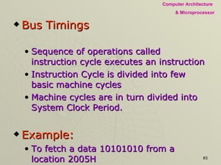
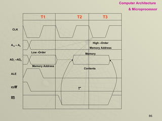
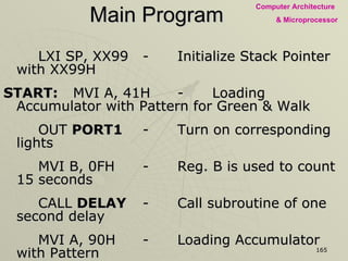
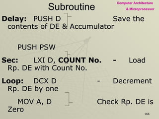
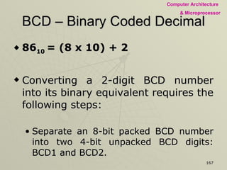
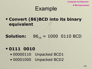
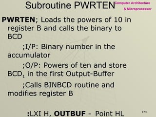
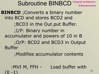
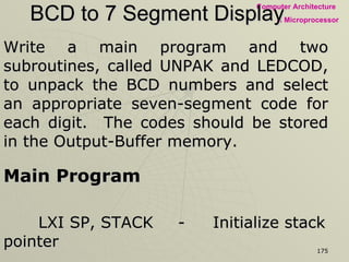
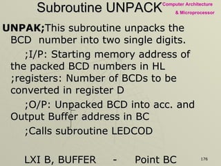
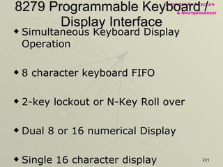
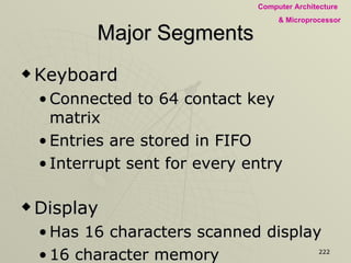
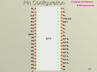
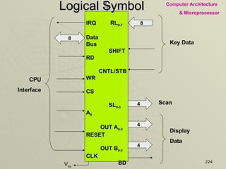
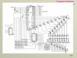
This document provides an overview of computer architecture and microprocessor concepts including:
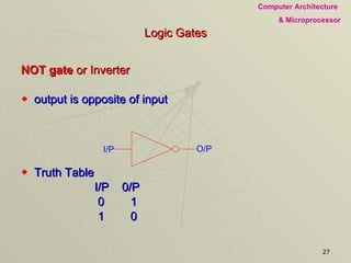
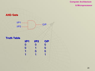
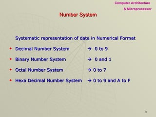
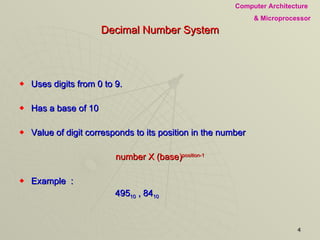
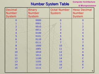
1. It discusses different number systems such as binary, decimal, hexadecimal and their conversions. It also covers logic gates, Boolean algebra and other digital logic concepts.
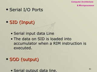
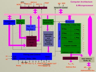
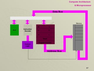
2. It introduces microprocessors and their general architecture. It discusses microprocessor operations such as memory reads/writes and I/O reads/writes.
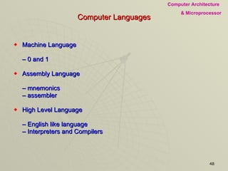
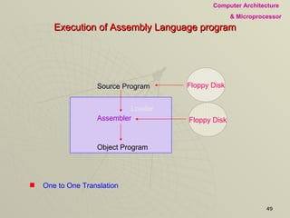
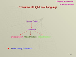
3. It covers computer languages from machine language to assembly and high-level languages. It also discusses compilers and interpreters.
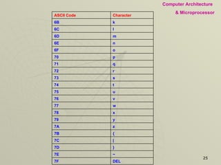
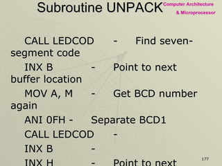
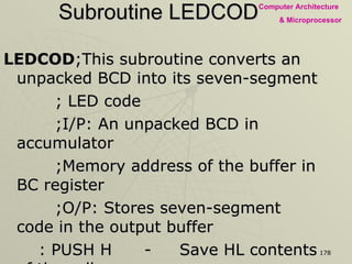
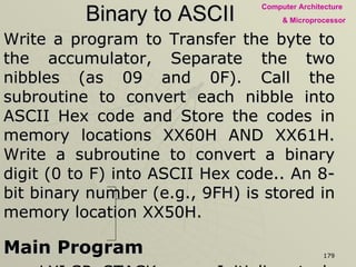
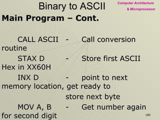
![U 55 T 54 S 53 R 52 Q 51 P 50 O 4F N 4E M 4D L 4C K 4B J 4A I 49 H 48 G 47 F 46 E 45 D 44 C 43 B 42 Character ASCII Code j 6B i 6A Characters ASCII h 69 g 67 f 66 e 65 d 64 c 63 b 62 a 61 - ( ) 5F ^ ( ) 5E ] 5D \ 5C [ 5B Z 5A Y 59 X 58 W 57 V 56](https://image.slidesharecdn.com/computerarchimp-100726095806-phpapp02/85/Computer-archi-mp-24-320.jpg)