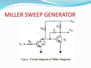
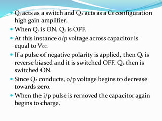
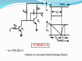
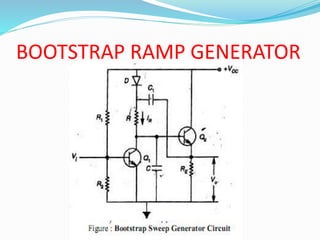
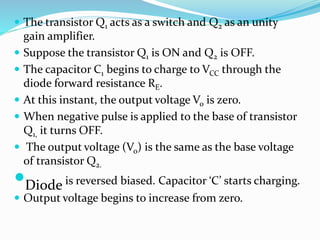
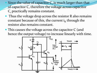
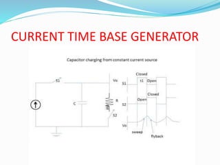
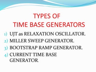
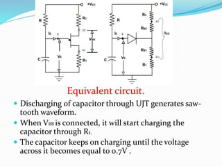
The document discusses various types of time base generators including UJT relaxation oscillator, Miller sweep generator, bootstrap ramp generator, and current time base generator. It describes the operation of each type, focusing on how capacitors charge and discharge to create output waveforms, with relevant formulas for calculating time and voltage. Key components and their functions are outlined, emphasizing how the output can be manipulated through control of circuit elements.

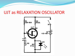
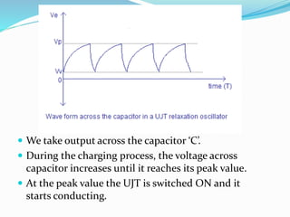
![ When the UJT starts conducting , the capacitor
starts discharging between emitter and B1.
When the capacitor voltage become zero, the
capacitor again starts charging.
The frequency of the o/p saw-tooth waveform can
be varied by changing the value of R1 resistor, since
this controls the time constant(R1C) of the
capacitor charging circuit.
FORMULA
t=2.3R1Clog10(1/1-ŋ)
t=R1Cloge(1/1-ŋ)
VC=VBB[1-e^(-t/R1C)]](https://image.slidesharecdn.com/typesoftimebasegenerators-150714175023-lva1-app6892/85/Types-of-time-base-generators-5-320.jpg)