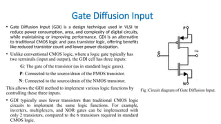
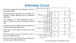
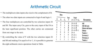
The document discusses the design and implementation of low power and area-efficient arithmetic circuits using the Gate Diffusion Input (GDI) technique, demonstrating improvements over traditional pass transistor logic (PTL). It highlights the development of an 8:1 multiplexer and a 4-bit arithmetic circuit, emphasizing reduced power consumption and propagation delays. The GDI technique allows for simpler designs with fewer transistors while significantly enhancing performance in various digital applications.
![INTRODUCTION
• In comparison to conventional CMOS design and existing PTL techniques, the GDI technique is
appropriate for the construction of quick, low-power circuits employing fewer transistors. [12].
• At the beginning of the 80s,CMOS logic was introduced and various design technique have been
developed to reduced delay propagation and speed up operation.
• Delay performance and power reduction is the important parameter for determining circuit efficiency in
VLSI digital circuits [28].
• The primary factor for high performance computing applications, image processing, portable [3]digital
equipment is need of low power.
• Numerous research efforts are prompted by the rapid development of portable digital applications, the
necessity for rising speed, small implementation, delay performance, and low power dissipation.
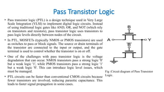
• Pass transistor logic is a type of logic that is common in low power digital circuitry (PTL) [15].Pass
transistors logic are designed by using NMOS alone. Different combinational selections are applied to
the nMOS transistors’ gates depending on the selection line.](https://image.slidesharecdn.com/gowtham-241001074330-c89346e2/85/design-and-implementation-of-Area-efficient-arithmetic-circuit-4-320.jpg)
![REFERENCE
• Abebe Diro, Haftu Reda, Naveen Chilamkurti, Abdun Mahmood, Noor Zaman, and Yunyoung Nam. Lightweight
authenticated-encryption scheme for internet of things based on publish-subscribe communication. IEEE Access, 8:60539–
60551, 2020.
• [2] Devaraj Ezhilarasan, Velluru S. Apoorva, and Nandhigam Ashok Vardhan. Syzygium cumini extract induced reactive
oxygen species-mediated apoptosis in human oral squamous carcinoma cells. Journal of Oral Pathology Medicine: Official
Publication of the International Association of Oral Pathologists and the American Academy of Oral Pathology, 48(2):115–
21, 2019.
• [3] Giovanni Fiengo. Alessandro di Gaeta. Angelo Palladino, and Veniero Giglio “Basic Concepts on GDI Systems.”
Common Rail System for GDI Engines, 2013.
• [4] Kumutha Jayaraman, Bethou Adhisivam, Saravanan Nallasivan, R. Gokul Krishnan, Chinnathambi Kamalarathnam,
Mangala Bharathi, Brent McSharry, et al. 38(2):198–202.
• [5] M. Kamaraju, K. Lal Kishore, and A. V. N. Tilak. Power optimized alu for efficient datapath. International Journal of
Computer Applications, 50(4):427–59, 2010.
• [6] Hammad Khawar, Tariq Rahim Soomro, and Muhammad Ayoub Kamal. Machine learning for internet of things-based
smart transportation networks. In Machine Learning for Societal Improvement, Modernization, and Progress, pages 112–134.
IGI Global, 2022.](https://image.slidesharecdn.com/gowtham-241001074330-c89346e2/85/design-and-implementation-of-Area-efficient-arithmetic-circuit-11-320.jpg)