Download to read offline
![Mrs. Sonika, Mr. Anshuman Singh / International Journal of Engineering Research and
Applications (IJERA) ISSN: 2248-9622 www.ijera.com
Vol. 3, Issue 1, January -February 2013, pp.482-484
Adaptive body biasing process compensation techniques for
Digital circuit
Mrs. Sonika*, Mr. Anshuman Singh**
*(lecturer in GNIT ,Greater Noida)
** (Assistant professor in NIET,Greater Noida)
ABSTRACT
The present invention relates generally drain coupled with functional failure, parametric failure
to the integrated circuits(ICs) & in particular to and/or device destruction.latch-up is an-undesirable
process, voltage & temperature(PVT) variations but controllable phenomenon.
in an ICs. PVT variations are critical factor that This Latchup may be prevented in two basic ways:•
hamper performance of Ics forexample PVT Latchup resistant CMOS process• Layout
variations can result in a change in setup &hold technique.[16]
times of synchronous circuits. Different
components of asynchronous circuit are driven 2.2 ELCTROSTATIC DISCHARGE
by a common system clock. Therefore any Electrostatic discharge is a subclass of the
change in setup or hold times corresponding to failure causes known as electrical overstress (EOS).
any one component causes an erroneous circuit The ESD events have four major stages: (1) charge
ouput.one technique to reduce PVT variations in generation (2) charge transfer (3) charge conduction
a circuit isbased on sensing the variations in the (4) charge induced damage.There are two basic
circuit &then taking the appropriate action to ways that circuits are protected: 1) Improve the
reducethese variations. unprotected elements 2) Add additional circuit
elements to divert the charge and clamp the voltage
Keywords: PVT compensation,Adaptive body most circuits use a combination of these three
biasing. techniques.
INTRODUCTION 2.3 ELECTROMIGRATION
In this era of ultra large scale integration Electro migration refers to the gradual
for a chip to be efficient , the I/O structures requires displacement of the metal atoms of a conductor as a
the circuit design expertise along with the result of the current flowing through that conductor.
knowledge of processes in detail. It is the I/O Electromigration can be prevented by:1) Proper
element which finally interfaces with the core signal design of the device 2) Good selection and
to the off chip environment. The i/o cells are placed deposition of the passivation
on the periphery of chip along with supply cells,
corners & fillers. The supply for the core is 2.4 SIMULTANEOUS SWITCHING NOISE
separated from supply of I/O’s because the noise (SSN):
that arise at the switching of the large output buffer This Switching Noise is called Simultaneous
.PAD is basically a sandwitch of various metal Switching Noise (SSN).SSN is studied byFeiYuan, Ph.D,
layers from where user can either receive the output P.Eng[8] and discussed lot of methods to reduce
or apply the input. The present work describes some it.SSN Reduction Techniques-Separate power and
of the basic design considerations for I/O pads. ground pins and pads for analog and digital circuits
Wherever possible, design option for smaller area whenever possible.
,low power &high speed has been comprehensively Corner pads will have long bond wire and there
dealt with. The emphasis is on having an idea of the inductance is very high.
various circuit elements involved in an I/O library
&an understanding of the behavior & their 3. DESIGN SPECIFICATION
performance & finally an optimized design is The specifications are a set of conditions
proposed for 3.3V tolerant bidirectional I/O. and functionality which are required by the
customer. For a designer it is necessary to observe
2. I/Os: problems & solutions specifications properly and then provide optimized
Main problems occur in I/Os are solution. The design must be ensured to work under
Latchup,Electrostatic discharge, electromigration& the process, temperature and Voltage variation.Here
simultaneous switching noise. by the design presented ensured to work under type
process, temperature variation from 0°C to 50°C ,
2.1 LATCH UP core supply variation from 1.1 to 1.2 and VDDE
Latch-up is a failure mechanism of CMOS variation from 3.0 V to 3.6 V. Other specifications
integrated circuits characterized by excessive current are delay, frequency of operation, VIL and VIH
482 | P a g e](https://image.slidesharecdn.com/bt31482484-130219231133-phpapp01/85/Bt31482484-1-320.jpg)
![Mrs. Sonika, Mr. Anshuman Singh / International Journal of Engineering Research and
Applications (IJERA) ISSN: 2248-9622 www.ijera.com
Vol. 3, Issue 1, January -February 2013, pp.482-484
Adaptive body biasing process compensation techniques for
Digital circuit
Mrs. Sonika*, Mr. Anshuman Singh**
*(lecturer in GNIT ,Greater Noida)
** (Assistant professor in NIET,Greater Noida)
ABSTRACT
The present invention relates generally drain coupled with functional failure, parametric failure
to the integrated circuits(ICs) & in particular to and/or device destruction.latch-up is an-undesirable
process, voltage & temperature(PVT) variations but controllable phenomenon.
in an ICs. PVT variations are critical factor that This Latchup may be prevented in two basic ways:•
hamper performance of Ics forexample PVT Latchup resistant CMOS process• Layout
variations can result in a change in setup &hold technique.[16]
times of synchronous circuits. Different
components of asynchronous circuit are driven 2.2 ELCTROSTATIC DISCHARGE
by a common system clock. Therefore any Electrostatic discharge is a subclass of the
change in setup or hold times corresponding to failure causes known as electrical overstress (EOS).
any one component causes an erroneous circuit The ESD events have four major stages: (1) charge
ouput.one technique to reduce PVT variations in generation (2) charge transfer (3) charge conduction
a circuit isbased on sensing the variations in the (4) charge induced damage.There are two basic
circuit &then taking the appropriate action to ways that circuits are protected: 1) Improve the
reducethese variations. unprotected elements 2) Add additional circuit
elements to divert the charge and clamp the voltage
Keywords: PVT compensation,Adaptive body most circuits use a combination of these three
biasing. techniques.
INTRODUCTION 2.3 ELECTROMIGRATION
In this era of ultra large scale integration Electro migration refers to the gradual
for a chip to be efficient , the I/O structures requires displacement of the metal atoms of a conductor as a
the circuit design expertise along with the result of the current flowing through that conductor.
knowledge of processes in detail. It is the I/O Electromigration can be prevented by:1) Proper
element which finally interfaces with the core signal design of the device 2) Good selection and
to the off chip environment. The i/o cells are placed deposition of the passivation
on the periphery of chip along with supply cells,
corners & fillers. The supply for the core is 2.4 SIMULTANEOUS SWITCHING NOISE
separated from supply of I/O’s because the noise (SSN):
that arise at the switching of the large output buffer This Switching Noise is called Simultaneous
.PAD is basically a sandwitch of various metal Switching Noise (SSN).SSN is studied byFeiYuan, Ph.D,
layers from where user can either receive the output P.Eng[8] and discussed lot of methods to reduce
or apply the input. The present work describes some it.SSN Reduction Techniques-Separate power and
of the basic design considerations for I/O pads. ground pins and pads for analog and digital circuits
Wherever possible, design option for smaller area whenever possible.
,low power &high speed has been comprehensively Corner pads will have long bond wire and there
dealt with. The emphasis is on having an idea of the inductance is very high.
various circuit elements involved in an I/O library
&an understanding of the behavior & their 3. DESIGN SPECIFICATION
performance & finally an optimized design is The specifications are a set of conditions
proposed for 3.3V tolerant bidirectional I/O. and functionality which are required by the
customer. For a designer it is necessary to observe
2. I/Os: problems & solutions specifications properly and then provide optimized
Main problems occur in I/Os are solution. The design must be ensured to work under
Latchup,Electrostatic discharge, electromigration& the process, temperature and Voltage variation.Here
simultaneous switching noise. by the design presented ensured to work under type
process, temperature variation from 0°C to 50°C ,
2.1 LATCH UP core supply variation from 1.1 to 1.2 and VDDE
Latch-up is a failure mechanism of CMOS variation from 3.0 V to 3.6 V. Other specifications
integrated circuits characterized by excessive current are delay, frequency of operation, VIL and VIH
482 | P a g e](https://image.slidesharecdn.com/bt31482484-130219231133-phpapp01/75/Bt31482484-1-2048.jpg)
![Mrs. Sonika, Mr. Anshuman Singh / International Journal of Engineering Research and
Applications (IJERA) ISSN: 2248-9622 www.ijera.com
Vol. 3, Issue 1, January -February 2013, pp.482-484
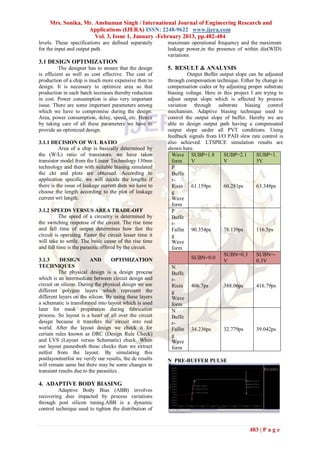
N Pre-buffer Rise References
[1] A.Amerasekeraand C.Durrury,ESD in
Silicon Integrated Circuit ,John Wiley &
Sons,1995.
[2] A.Amerasekeraet.,Al.,”ESD failure Modes
: Characteristics Mechanism and Process
Influences” IEEE Trans. Electron
Devices,Vol.39,No2,pp.430-436,feb1992.
[3] A.Amerasekera and C.Duvvury ” The
Impact of technology scaling on ESD
Simulation Waveform of Output Buffer Robustness and Protection Circuit design ,”
Output Waveform Pulse: Proc.EOS/ESD Symp.,1994,pp 237-245.
[4] C.Duvvury and A.Amerasekera,” ESD
issued for advanced CMOSTechnologies ,”
Microelectronics
Reliability,Vol36,No7,1996.
[5] Canh Q Tran,Hiroshi Kawaguchi and
Takayasu Sakurai .” Low Power High
Speed Level Shifter design for Block-Level
dynamic voltage scaling environment ,”
University of Tokyo.
Output Waveform Rising [6] Craig Brunty and Laszlo Gal ,” Optimum
Tapered Buffer” IEEEJSSC Vol 27 Jan
1992.
[7] C.R. Parthasarthy,” Investigation of Slew
Rate Control in the buffersof HCMOSS I/O
library,” Library development
group,Central R&D ,ST Microelectronics
Gr.Noida.
[8] FeiYuan ,Ph.D,P.Engg,” Simultaneous
Switching Noise(SSN),” Department of
Electrical and computer
Engg,RyersonUniversity,Toronto,Canada.
[9] Jose Rocha,MarcelinoSantos,J.MDores
Output Waveform Falling Costa and Floriberto Lima,” High Voltage
Tolerent Level Shifters and Logic Gates in
standard low voltage CMOS Technology .
[10] J.S.Shor,Y.Afek and E.Engel,”I/O buffer
for high performance ,low power
application ,” CICC,pp,595-598,May,1997.
[11] J.E.Vinson and J.J.Liou,” Electrostatic
discharge in semiconductor devices
,protection technique “Proceeding of
IEEE,Vol 88,2000.
CONCLUSION:
Due to change in Substrate Voltage Slope of
the output Curve changesIncrease inSubstrate Bias
Voltage Decrease in Rise (tr) and Fall (tf) time of
output waveform. The Complete design of the
compensated circuit for an I/O buffer is presented
with the cost of area and process mask generation
time. The system will work at hundreds of MHz and
presents same quality of output signal and hence
reduces the noise encounters due to change in
process design.
484 | P a g e](https://image.slidesharecdn.com/bt31482484-130219231133-phpapp01/85/Bt31482484-3-320.jpg)

This document summarizes some key challenges for digital circuits related to process, voltage, and temperature variations. It discusses techniques to prevent latchup and electrostatic discharge issues in integrated circuits. It also describes simultaneous switching noise that can occur when large numbers of circuits switch simultaneously. The document proposes using adaptive body biasing techniques to compensate for PVT variations and control output slope under different conditions. Simulation results show this approach can adjust rising and falling times of an output buffer for different substrate bias voltage conditions.