CMOS VLSI Design4th Ed.
1: Circuits & Layout 4
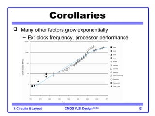
Growth Rate
53% compound annual growth rate over 50 years
– No other technology has grown so fast so long
Driven by miniaturization of transistors
– Smaller is cheaper, faster, lower in power!
– Revolutionary effects on society
[Moore65]
Electronics Magazine
5.
CMOS VLSI Design4th Ed.
1: Circuits & Layout 5
Annual Sales
>1019
transistors manufactured in 2008
– 1 billion for every human on the planet
6.
CMOS VLSI Design4th Ed.
1: Circuits & Layout 6
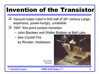
Invention of the Transistor
Vacuum tubes ruled in first half of 20th
century Large,
expensive, power-hungry, unreliable
1947: first point contact transistor
– John Bardeen and Walter Brattain at Bell Labs
– See Crystal Fire
by Riordan, Hoddeson
AT&T Archives.
Reprinted with
permission.
7.
CMOS VLSI Design4th Ed.
1: Circuits & Layout 7
Transistor Types
Bipolar transistors
– npn or pnp silicon structure
– Small current into very thin base layer controls
large currents between emitter and collector
– Base currents limit integration density
Metal Oxide Semiconductor Field Effect Transistors
– nMOS and pMOS MOSFETS
– Voltage applied to insulated gate controls current
between source and drain
– Low power allows very high integration
CMOS VLSI Design4th Ed.
1: Circuits & Layout 13
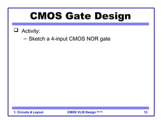
CMOS Gate Design
Activity:
– Sketch a 4-input CMOS NOR gate
A
B
C
D
Y
14.
CMOS VLSI Design4th Ed.
1: Circuits & Layout 14
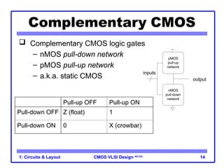
Complementary CMOS
Complementary CMOS logic gates
– nMOS pull-down network
– pMOS pull-up network
– a.k.a. static CMOS
pMOS
pull-up
network
output
inputs
nMOS
pull-down
network
Pull-up OFF Pull-up ON
Pull-down OFF Z (float) 1
Pull-down ON 0 X (crowbar)
15.
CMOS VLSI Design4th Ed.
1: Circuits & Layout 15
Series and Parallel
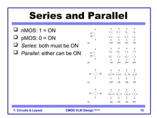
nMOS: 1 = ON
pMOS: 0 = ON
Series: both must be ON
Parallel: either can be ON
(a)
a
b
a
b
g1
g2
0
0
a
b
0
1
a
b
1
0
a
b
1
1
OFF OFF OFF ON
(b)
a
b
a
b
g1
g2
0
0
a
b
0
1
a
b
1
0
a
b
1
1
ON OFF OFF OFF
(c)
a
b
a
b
g1 g2 0 0
OFF ON ON ON
(d) ON ON ON OFF
a
b
0
a
b
1
a
b
1
1 0 1
a
b
0 0
a
b
0
a
b
1
a
b
1
1 0 1
a
b
g1 g2
16.
CMOS VLSI Design4th Ed.
1: Circuits & Layout 16
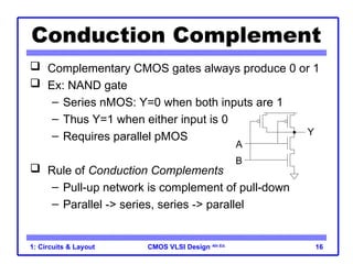
Conduction Complement
Complementary CMOS gates always produce 0 or 1
Ex: NAND gate
– Series nMOS: Y=0 when both inputs are 1
– Thus Y=1 when either input is 0
– Requires parallel pMOS
Rule of Conduction Complements
– Pull-up network is complement of pull-down
– Parallel -> series, series -> parallel
A
B
Y
17.
CMOS VLSI Design4th Ed.
1: Circuits & Layout 17
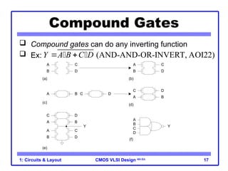
Compound Gates
Compound gates can do any inverting function
Ex: (AND-AND-OR-INVERT, AOI22)
Y A B C D
A
B
C
D
A
B
C
D
A B C D
A B
C D
B
D
Y
A
C
A
C
A
B
C
D
B
D
Y
(a)
(c)
(e)
(b)
(d)
(f)
18.
CMOS VLSI Design4th Ed.
1: Circuits & Layout 18
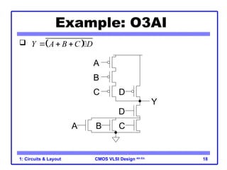
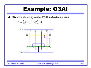
Example: O3AI
Y A B C D
A B
Y
C
D
D
C
B
A
19.
CMOS VLSI Design4th Ed.
1: Circuits & Layout 19
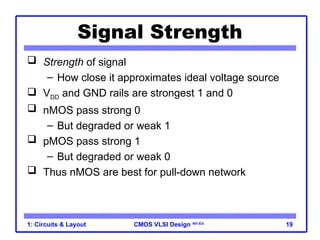
Signal Strength
Strength of signal
– How close it approximates ideal voltage source
VDD and GND rails are strongest 1 and 0
nMOS pass strong 0
– But degraded or weak 1
pMOS pass strong 1
– But degraded or weak 0
Thus nMOS are best for pull-down network
20.
CMOS VLSI Design4th Ed.
1: Circuits & Layout 20
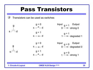
Pass Transistors
Transistors can be used as switches
g = 0
s d
g = 1
s d
0 strong 0
Input Output
1 degraded 1
g = 0
s d
g = 1
s d
0 degraded 0
Input Output
strong 1
g = 1
g = 1
g = 0
g = 0
1
g
s d
g
s d
21.
CMOS VLSI Design4th Ed.
1: Circuits & Layout 21
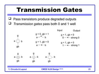
Transmission Gates
Pass transistors produce degraded outputs
Transmission gates pass both 0 and 1 well
g = 0, gb = 1
a b
g = 1, gb = 0
a b
0 strong 0
Input Output
1 strong 1
g
gb
a b
a b
g
gb
a b
g
gb
a b
g
gb
g = 1, gb = 0
g = 1, gb = 0
22.
CMOS VLSI Design4th Ed.
1: Circuits & Layout 22
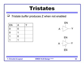
Tristates
Tristate buffer produces Z when not enabled
EN A Y
0 0 Z
0 1 Z
1 0 0
1 1 1
A Y
EN
A Y
EN
EN
23.
CMOS VLSI Design4th Ed.
1: Circuits & Layout 23
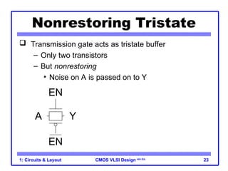
Nonrestoring Tristate
Transmission gate acts as tristate buffer
– Only two transistors
– But nonrestoring
• Noise on A is passed on to Y
A Y
EN
EN
24.
CMOS VLSI Design4th Ed.
1: Circuits & Layout 24
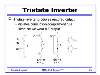
Tristate Inverter
Tristate inverter produces restored output
– Violates conduction complement rule
– Because we want a Z output
A
Y
EN
A
Y
EN = 0
Y = 'Z'
Y
EN = 1
Y = A
A
EN
25.
CMOS VLSI Design4th Ed.
1: Circuits & Layout 25
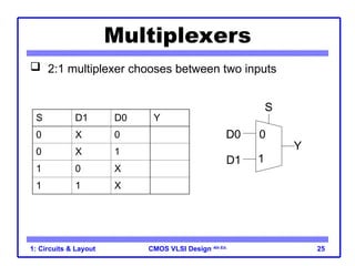
Multiplexers
2:1 multiplexer chooses between two inputs
S D1 D0 Y
0 X 0 0
0 X 1 1
1 0 X 0
1 1 X 1
0
1
S
D0
D1
Y
26.
CMOS VLSI Design4th Ed.
1: Circuits & Layout 26
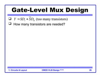
Gate-Level Mux Design
How many transistors are needed? 20
1 0 (too many transistors)
Y SD SD
4
4
D1
D0
S Y
4
2
2
2 Y
2
D1
D0
S
27.
CMOS VLSI Design4th Ed.
1: Circuits & Layout 27
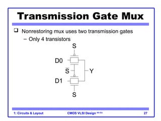
Transmission Gate Mux
Nonrestoring mux uses two transmission gates
– Only 4 transistors
S
S
D0
D1
Y
S
28.
CMOS VLSI Design4th Ed.
1: Circuits & Layout 28
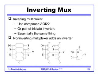
Inverting Mux
Inverting multiplexer
– Use compound AOI22
– Or pair of tristate inverters
– Essentially the same thing
Noninverting multiplexer adds an inverter
S
D0 D1
Y
S
D0
D1
Y
0
1
S
Y
D0
D1
S
S
S
S
S
S
29.
CMOS VLSI Design4th Ed.
1: Circuits & Layout 29
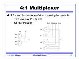
4:1 Multiplexer
4:1 mux chooses one of 4 inputs using two selects
– Two levels of 2:1 muxes
– Or four tristates
S0
D0
D1
0
1
0
1
0
1
Y
S1
D2
D3
D0
D1
D2
D3
Y
S1S0 S1S0 S1S0 S1S0
30.
CMOS VLSI Design4th Ed.
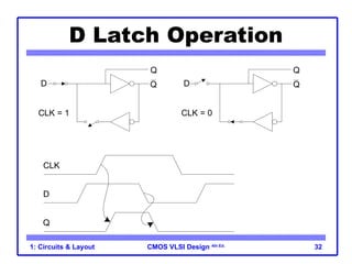
1: Circuits & Layout 30
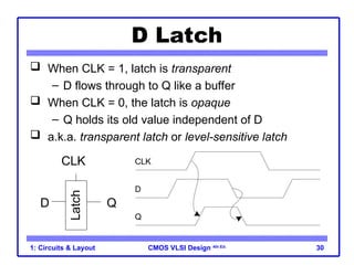
D Latch
When CLK = 1, latch is transparent
– D flows through to Q like a buffer
When CLK = 0, the latch is opaque
– Q holds its old value independent of D
a.k.a. transparent latch or level-sensitive latch
CLK
D Q
Latch
D
CLK
Q
31.
CMOS VLSI Design4th Ed.
1: Circuits & Layout 31
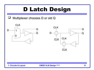
D Latch Design
Multiplexer chooses D or old Q
1
0
D
CLK
Q
CLK
CLK
CLK
CLK
D
Q Q
Q
32.
CMOS VLSI Design4th Ed.
1: Circuits & Layout 32
D Latch Operation
CLK = 1
D Q
Q
CLK = 0
D Q
Q
D
CLK
Q
33.
CMOS VLSI Design4th Ed.
1: Circuits & Layout 33
D Flip-flop
When CLK rises, D is copied to Q
At all other times, Q holds its value
a.k.a. positive edge-triggered flip-flop, master-slave
flip-flop
Flop
CLK
D Q
D
CLK
Q
34.
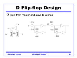
CMOS VLSI Design4th Ed.
1: Circuits & Layout 34
D Flip-flop Design
Built from master and slave D latches
QM
CLK
CLK
CLK
CLK
Q
CLK
CLK
CLK
CLK
D
Latch
Latch
D Q
QM
CLK
CLK
35.
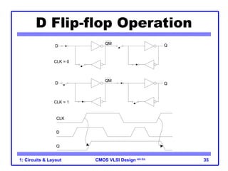
CMOS VLSI Design4th Ed.
1: Circuits & Layout 35
D Flip-flop Operation
CLK = 1
D
CLK = 0
Q
D
QM
QM
Q
D
CLK
Q
36.
CMOS VLSI Design4th Ed.
1: Circuits & Layout 36
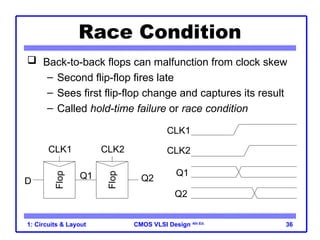
Race Condition
Back-to-back flops can malfunction from clock skew
– Second flip-flop fires late
– Sees first flip-flop change and captures its result
– Called hold-time failure or race condition
CLK1
D
Q1
Flop
Flop
CLK2
Q2
CLK1
CLK2
Q1
Q2
37.
CMOS VLSI Design4th Ed.
1: Circuits & Layout 37
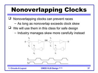
Nonoverlapping Clocks
Nonoverlapping clocks can prevent races
– As long as nonoverlap exceeds clock skew
We will use them in this class for safe design
– Industry manages skew more carefully instead
1
1
1
1
2
2
2
2
2
1
QM
Q
D
38.
CMOS VLSI Design4th Ed.
1: Circuits & Layout 38
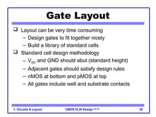
Gate Layout
Layout can be very time consuming
– Design gates to fit together nicely
– Build a library of standard cells
Standard cell design methodology
– VDD and GND should abut (standard height)
– Adjacent gates should satisfy design rules
– nMOS at bottom and pMOS at top
– All gates include well and substrate contacts
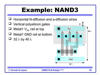
CMOS VLSI Design4th Ed.
1: Circuits & Layout 40
Example: NAND3
Horizontal N-diffusion and p-diffusion strips
Vertical polysilicon gates
Metal1 VDD rail at top
Metal1 GND rail at bottom
32 by 40
41.
CMOS VLSI Design4th Ed.
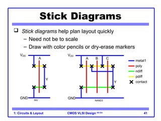
1: Circuits & Layout 41
Stick Diagrams
Stick diagrams help plan layout quickly
– Need not be to scale
– Draw with color pencils or dry-erase markers
c
A
VDD
GND
Y
A
VDD
GND
B C
Y
INV
metal1
poly
ndiff
pdiff
contact
NAND3
42.
CMOS VLSI Design4th Ed.
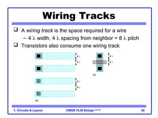
1: Circuits & Layout 42
Wiring Tracks
A wiring track is the space required for a wire
– 4 width, 4 spacing from neighbor = 8 pitch
Transistors also consume one wiring track
43.
CMOS VLSI Design4th Ed.
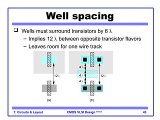
1: Circuits & Layout 43
Well spacing
Wells must surround transistors by 6
– Implies 12 between opposite transistor flavors
– Leaves room for one wire track
44.
CMOS VLSI Design4th Ed.
1: Circuits & Layout 44
32
40
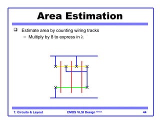
Area Estimation
Estimate area by counting wiring tracks
– Multiply by 8 to express in
45.
CMOS VLSI Design4th Ed.
1: Circuits & Layout 45
Example: O3AI
Sketch a stick diagram for O3AI and estimate area
–
Y A B C D
A
VDD
GND
B C
Y
D
6 tracks =
48
5 tracks =
40
![CMOS VLSI Design 4th Ed.
1: Circuits & Layout 3
A Brief History
1958: First integrated circuit
– Flip-flop using two transistors
– Built by Jack Kilby at Texas
Instruments
2010
– Intel Core i7 processor
• 2.3 billion transistors
– 64 Gb Flash memory
• > 16 billion transistors
Courtesy Texas Instruments
[Trinh09]
© 2009 IEEE](https://image.slidesharecdn.com/lect1-cktlay-250306013116-5b85704d/85/CMOS-VLSI-Design-Lecture-1-Circuit-Layout-3-320.jpg)
![CMOS VLSI Design 4th Ed.
1: Circuits & Layout 4
Growth Rate
53% compound annual growth rate over 50 years
– No other technology has grown so fast so long
Driven by miniaturization of transistors
– Smaller is cheaper, faster, lower in power!
– Revolutionary effects on society
[Moore65]
Electronics Magazine](https://image.slidesharecdn.com/lect1-cktlay-250306013116-5b85704d/85/CMOS-VLSI-Design-Lecture-1-Circuit-Layout-4-320.jpg)

![CMOS VLSI Design 4th Ed.
1: Circuits & Layout 8
1970’s processes usually had only nMOS transistors
– Inexpensive, but consume power while idle
1980s-present: CMOS processes for low idle power
MOS Integrated Circuits
Intel 1101 256-bit SRAM Intel 4004 4-bit Proc
[Vadasz69]
© 1969 IEEE.
Intel
Museum.
Reprinted
with
permission.](https://image.slidesharecdn.com/lect1-cktlay-250306013116-5b85704d/85/CMOS-VLSI-Design-Lecture-1-Circuit-Layout-8-320.jpg)
![CMOS VLSI Design 4th Ed.
1: Circuits & Layout 9
Moore’s Law: Then
1965: Gordon Moore plotted transistor on each chip
– Fit straight line on semilog scale
– Transistor counts have doubled every 26 months
Integration Levels
SSI: 10 gates
MSI: 1000 gates
LSI: 10,000 gates
VLSI: > 10k gates
[Moore65]
Electronics Magazine](https://image.slidesharecdn.com/lect1-cktlay-250306013116-5b85704d/85/CMOS-VLSI-Design-Lecture-1-Circuit-Layout-9-320.jpg)