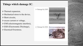
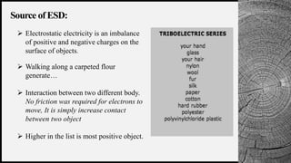
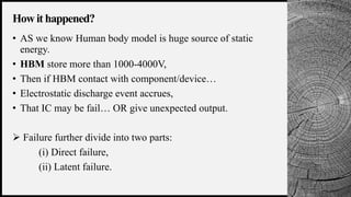
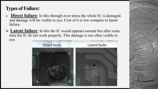
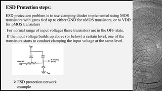
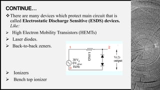
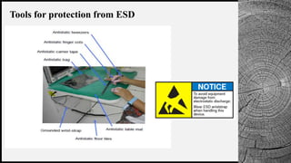
WOODGROVE
BANK 1
GOVERNMENT ENGINNERING
COLLEGE
RAJKOT
Electronic & Communication Dept,
Subject: VLSI Design &Technology
ESD Protection
(ElectroStaticsDischarge)
Present by,
Bhargav Borisagar
(160200111012)
WOODGROVE
BANK
Thermal expansion,
Mechanical stress to the device,
Short circuits,
excess current or voltage,
EMI (electromagnetic interfere),
ESD (Electrostatic Discharge),
Electrical Overstress.
 Damage by ESD:
 Damage by EOS:
3
Things which damage IC:
WOODGROVE
BANK
Source of ESD:
4
 Electrostatic electricity is an imbalance
of positive and negative charges on the
surface of objects.
 Walking along a carpeted flour
generate…
 Interaction between two different body.
No friction was required for electrons to
move, It is simply increase contact
between two object
 Higher in the list is most positive object.
WOODGROVE
BANK
• AS we know Human body model is huge source of static
energy.
• HBM store more than 1000-4000V,
• Then if HBM contact with component/device…
• Electrostatic discharge event accrues,
• That IC may be fail… OR give unexpected output.
 Failure further divide into two parts:
(i) Direct failure,
(ii) Latent failure.
5
How it happened?
WOODGROVE
BANK 6
 Direct failure: In this through over stress the whole IC is damaged.
and damage will be visible to eye. Cost of it is low compare to latent
failure.
 Latent failure: In this the IC would appears normal but after some
time the IC do not work properly. This damage is not often visible to
eye.
Types of Failure:
WOODGROVE
BANK 7
ESD protection problem is to use clamping diodes implemented using MOS
transistors with gates tied up to either GND for nMOS transistors, or to VDD
for pMOS transistors
For normal range of input voltages these transistors are in the OFF state.
If the input voltage builds up above (or below) a certain level, one of the
transistors starts to conduct clamping the input voltage at the same level.
ESD Protection steps:
ESD protection network
example
WOODGROVE
BANK
CONTINUE…
There are many devices which protect main circuit that is
called Electrostatic Discharge Sensitive (ESDS) devices.
Like:
 High Electron Mobility Transistors (HEMTs)
 Laser diodes.
 Back-to-back zeners.
 Ionizers
 Bench top ionizer
8
WOODGROVE
BANK 9
Tools for protection from ESD
WOODGROVE
BANK
THANK YOU
Any
QUESTIONS???

Esd protection

  • 1.
    WOODGROVE BANK 1 GOVERNMENT ENGINNERING COLLEGE RAJKOT Electronic& Communication Dept, Subject: VLSI Design &Technology
  • 2.
  • 3.
    WOODGROVE BANK Thermal expansion, Mechanical stressto the device, Short circuits, excess current or voltage, EMI (electromagnetic interfere), ESD (Electrostatic Discharge), Electrical Overstress.  Damage by ESD:  Damage by EOS: 3 Things which damage IC:
  • 4.
    WOODGROVE BANK Source of ESD: 4 Electrostatic electricity is an imbalance of positive and negative charges on the surface of objects.  Walking along a carpeted flour generate…  Interaction between two different body. No friction was required for electrons to move, It is simply increase contact between two object  Higher in the list is most positive object.
  • 5.
    WOODGROVE BANK • AS weknow Human body model is huge source of static energy. • HBM store more than 1000-4000V, • Then if HBM contact with component/device… • Electrostatic discharge event accrues, • That IC may be fail… OR give unexpected output.  Failure further divide into two parts: (i) Direct failure, (ii) Latent failure. 5 How it happened?
  • 6.
    WOODGROVE BANK 6  Directfailure: In this through over stress the whole IC is damaged. and damage will be visible to eye. Cost of it is low compare to latent failure.  Latent failure: In this the IC would appears normal but after some time the IC do not work properly. This damage is not often visible to eye. Types of Failure:
  • 7.
    WOODGROVE BANK 7 ESD protectionproblem is to use clamping diodes implemented using MOS transistors with gates tied up to either GND for nMOS transistors, or to VDD for pMOS transistors For normal range of input voltages these transistors are in the OFF state. If the input voltage builds up above (or below) a certain level, one of the transistors starts to conduct clamping the input voltage at the same level. ESD Protection steps: ESD protection network example
  • 8.
    WOODGROVE BANK CONTINUE… There are manydevices which protect main circuit that is called Electrostatic Discharge Sensitive (ESDS) devices. Like:  High Electron Mobility Transistors (HEMTs)  Laser diodes.  Back-to-back zeners.  Ionizers  Bench top ionizer 8
  • 9.
    WOODGROVE BANK 9 Tools forprotection from ESD
  • 10.

Editor's Notes

  • #6 Q = CV V = Q/C V = It/C Let us consider a modest 1pF capacitor, in which, this 1nC charge is put (can be through a 100uA current for a millisec). This results in V=10^(-9) ________=1000V 10^(-12) SiO2 breakdown voltage is 10^(9)volts/meter. If gate oxide is about 0.1um thick, say; Maximum allowable voltage is   10^(9)*[0.1/10^6] = 100V. This can easily be generated by walking across a carpet!! A human touch can produce instanteous voltages of 20,000 volts!