This document outlines the key concepts covered in the first lecture of an introduction to CMOS VLSI design course, including:
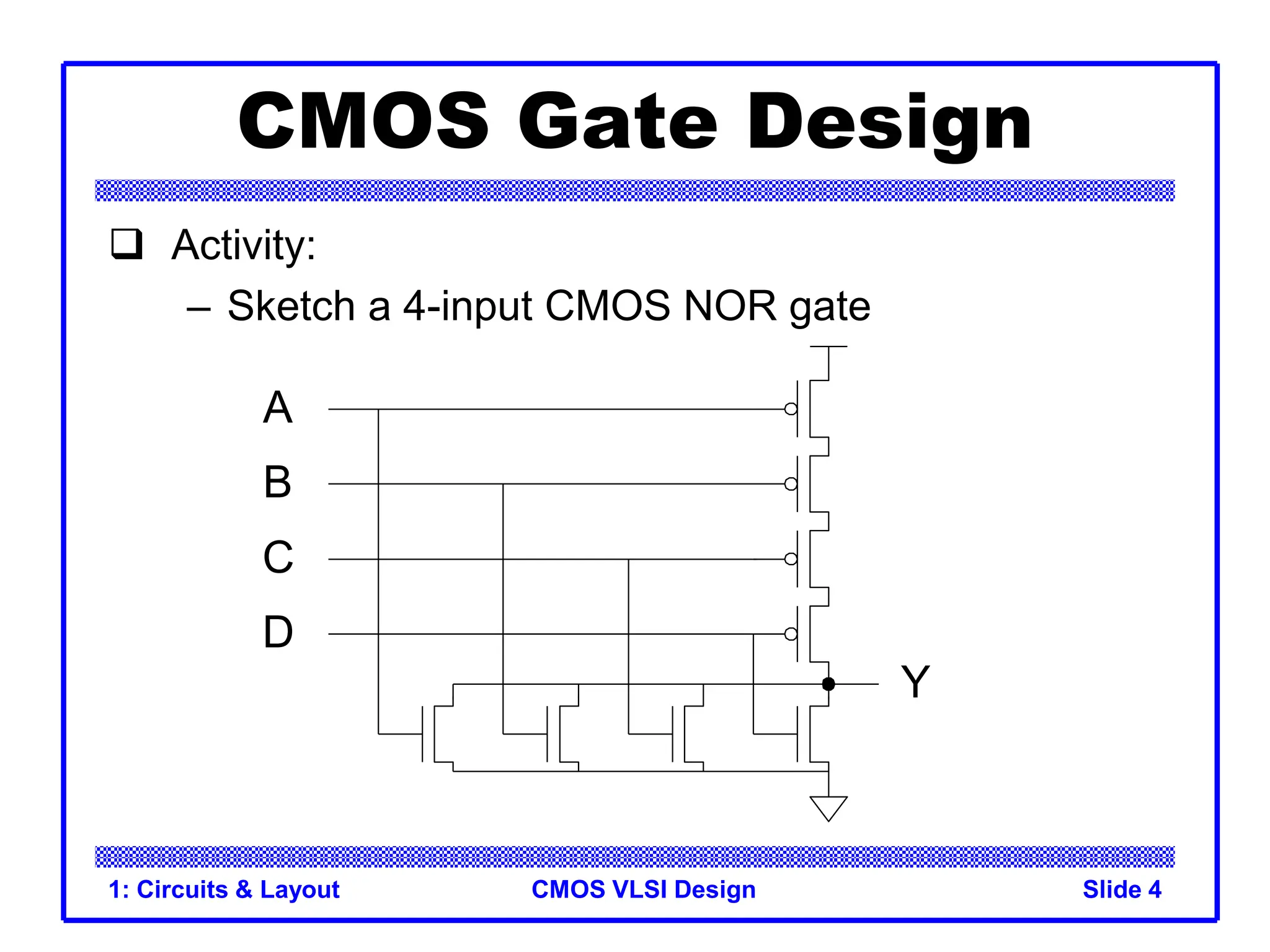
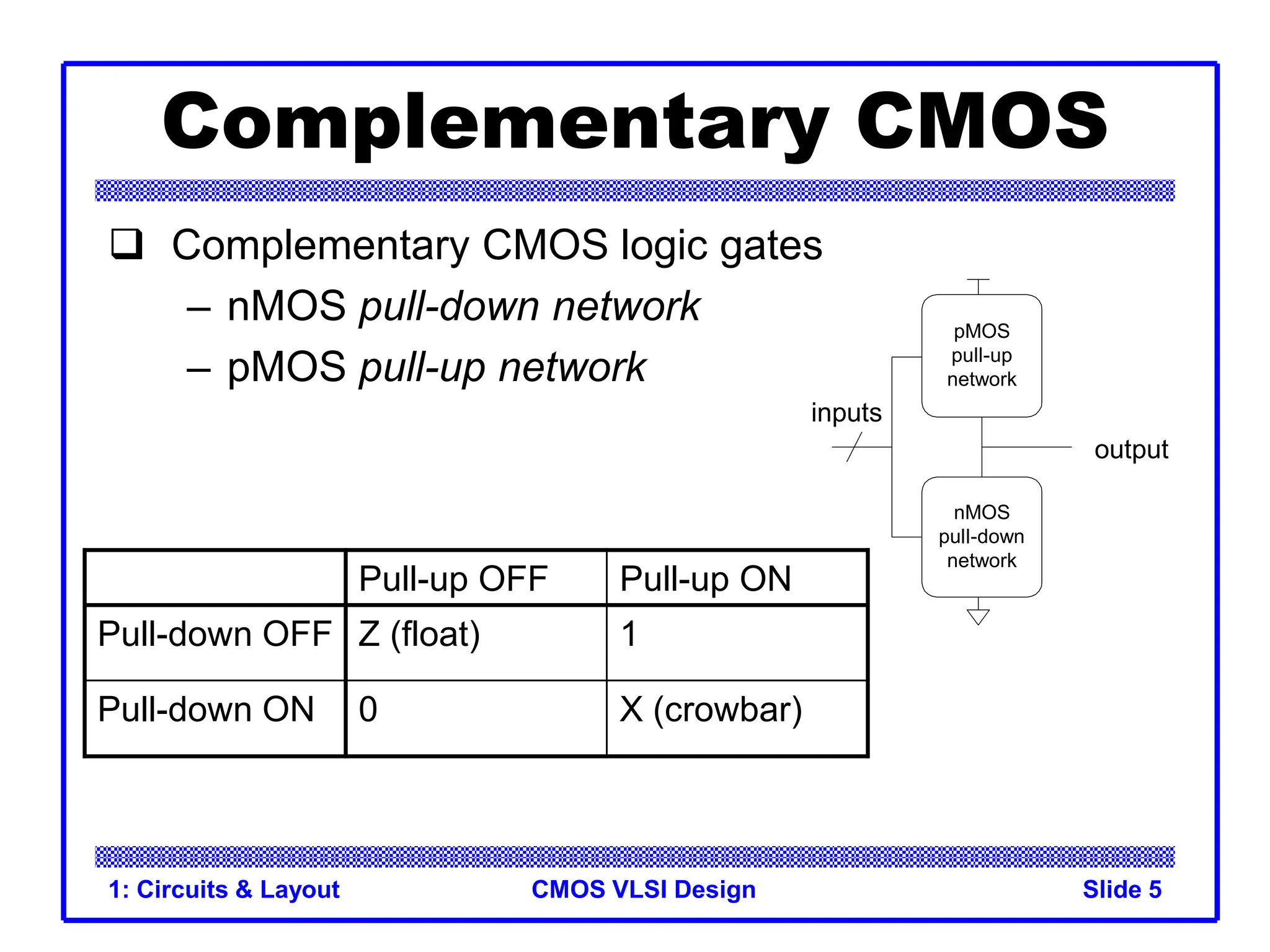
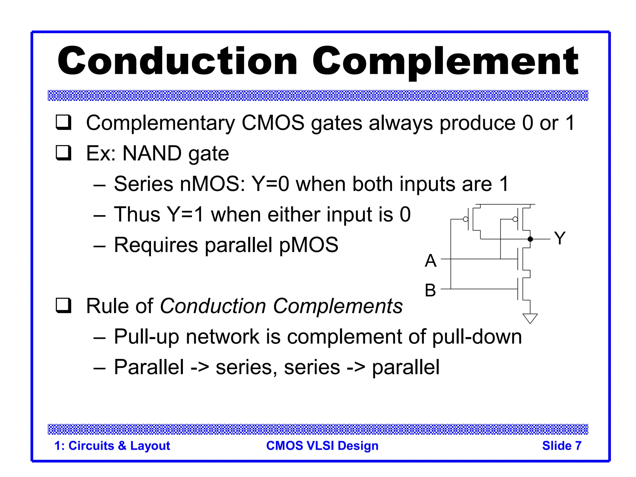
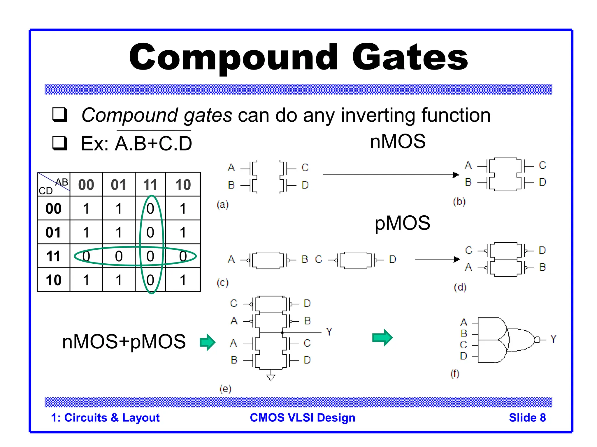
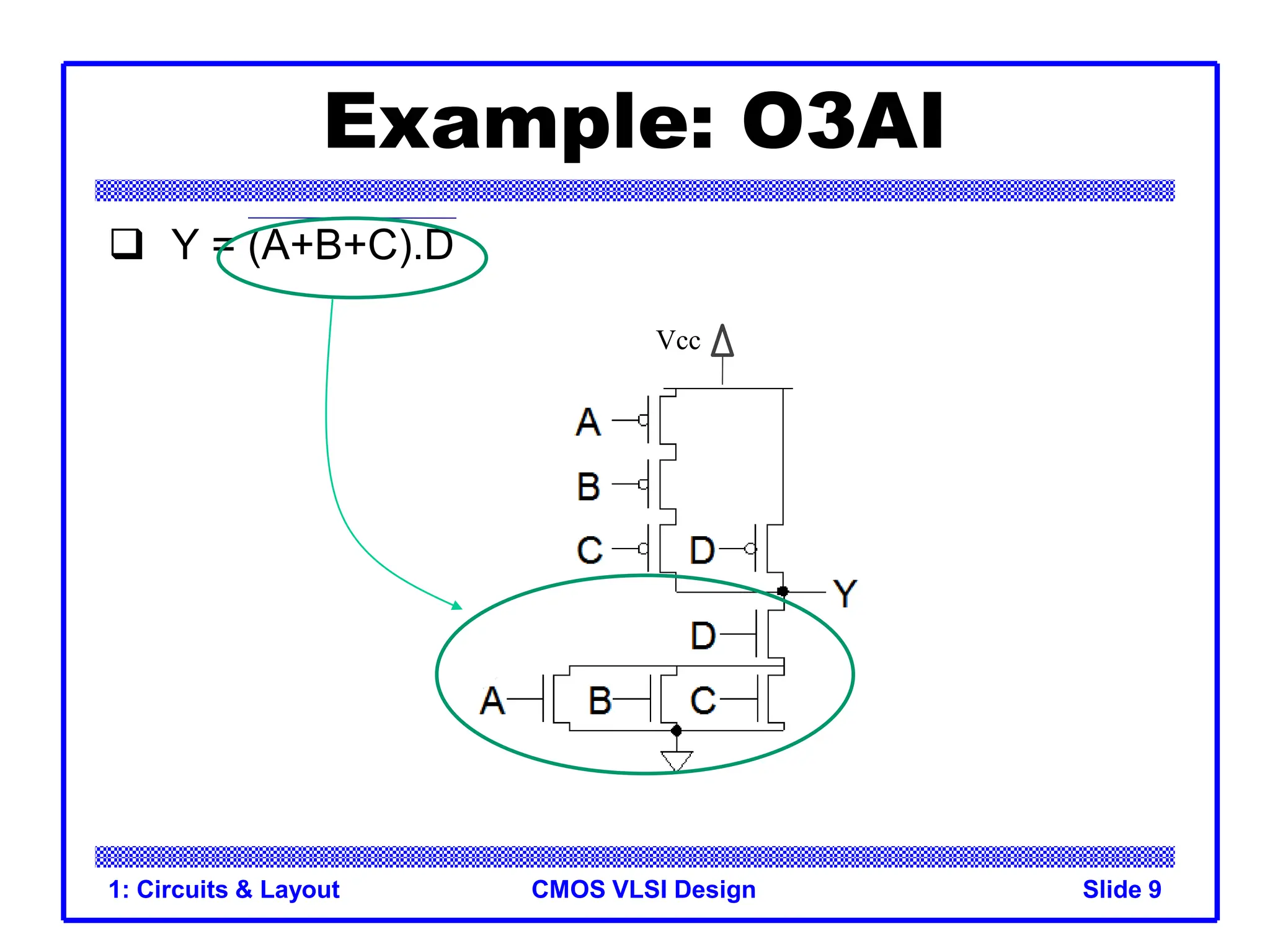
1) The design of basic CMOS logic gates using nMOS pull-down and pMOS pull-up networks along with the concept of conduction complements.
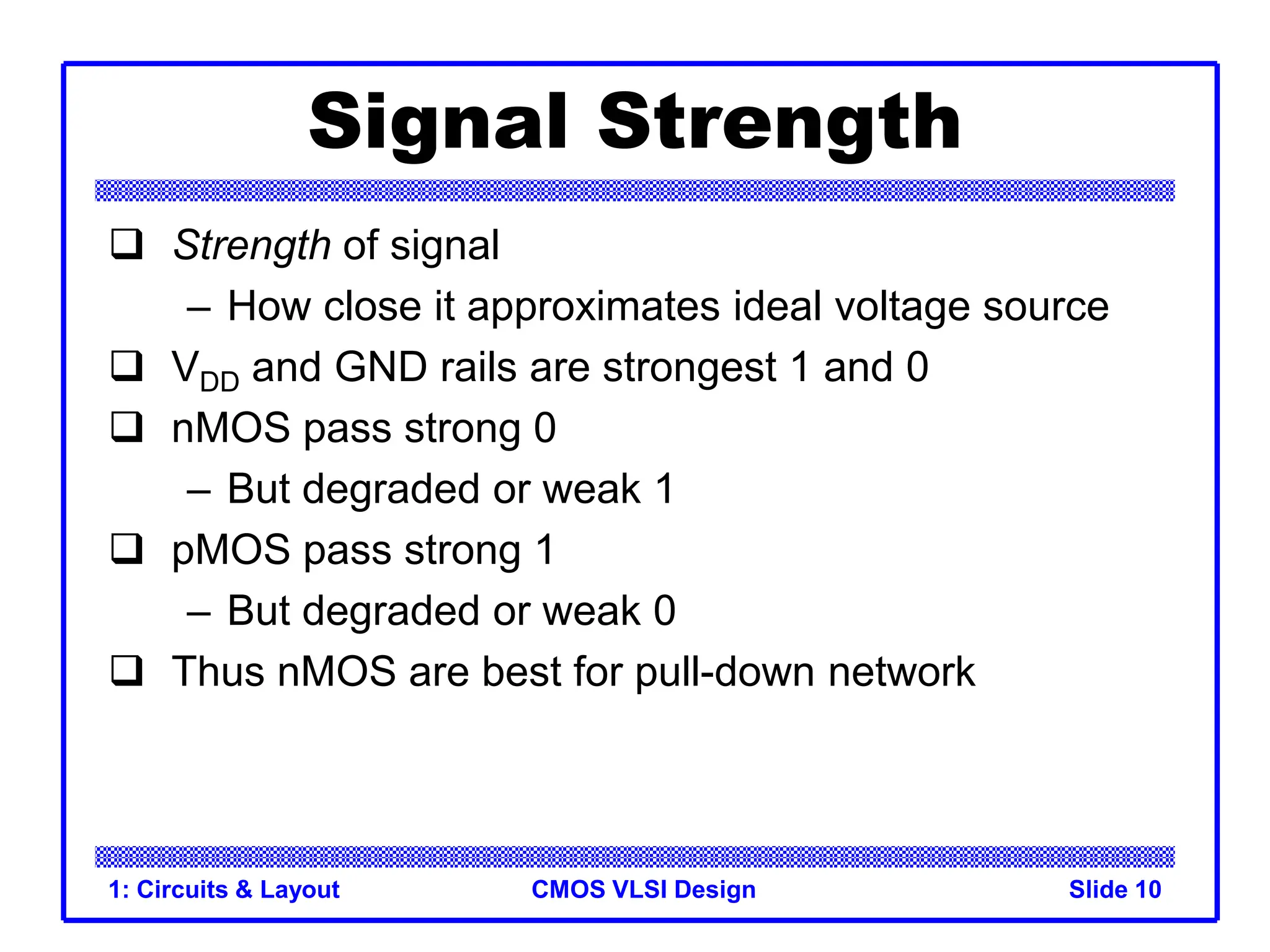
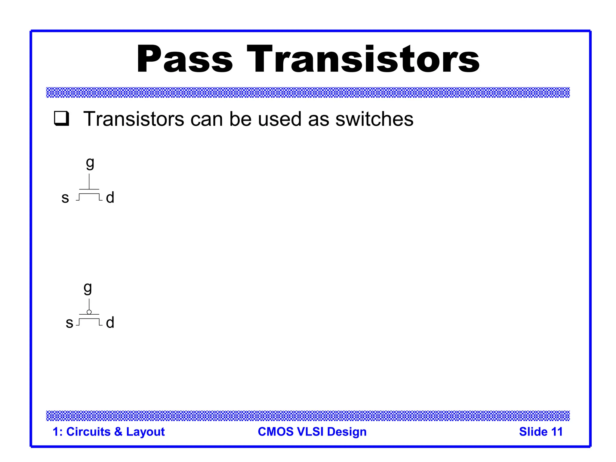
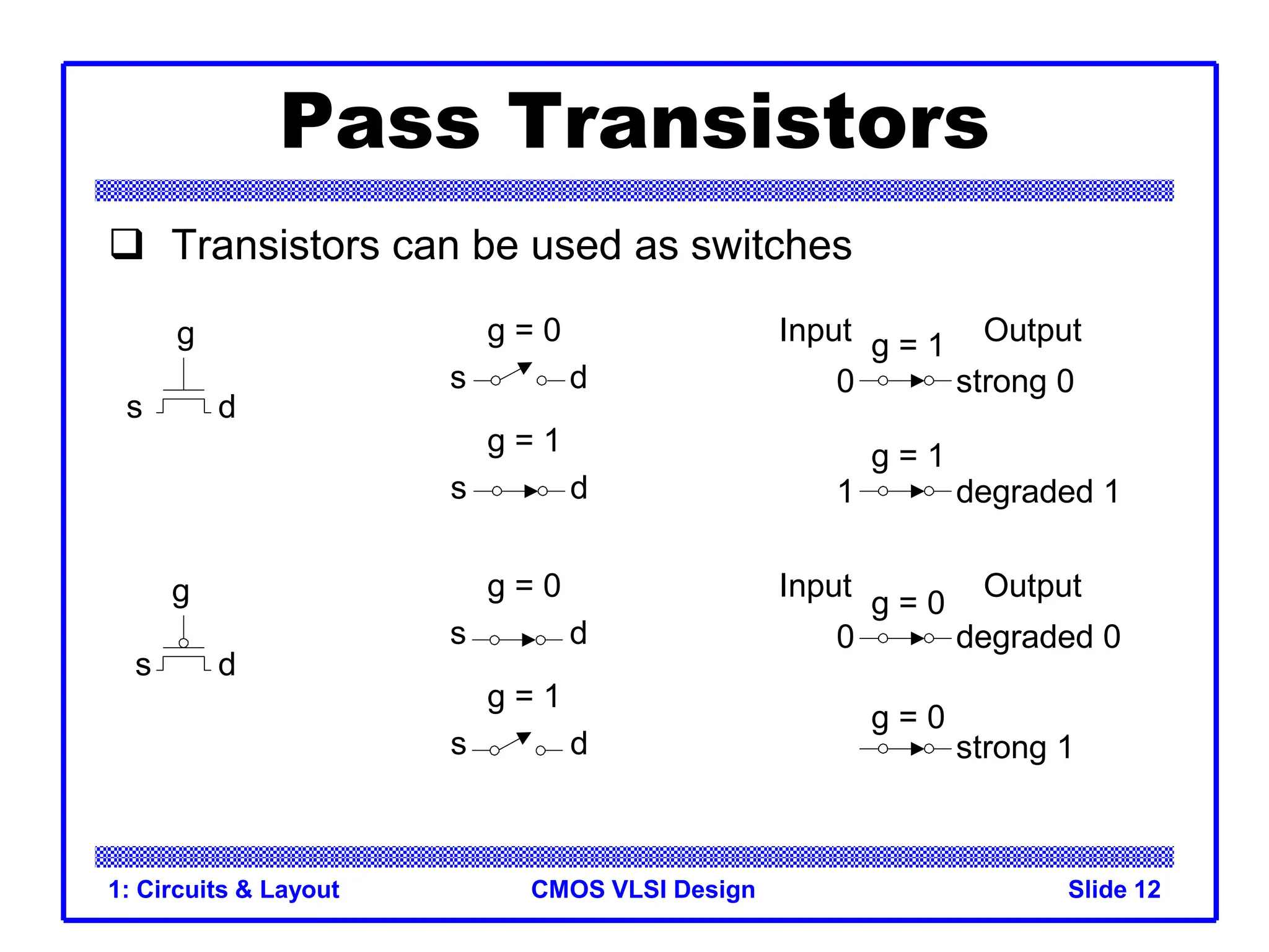
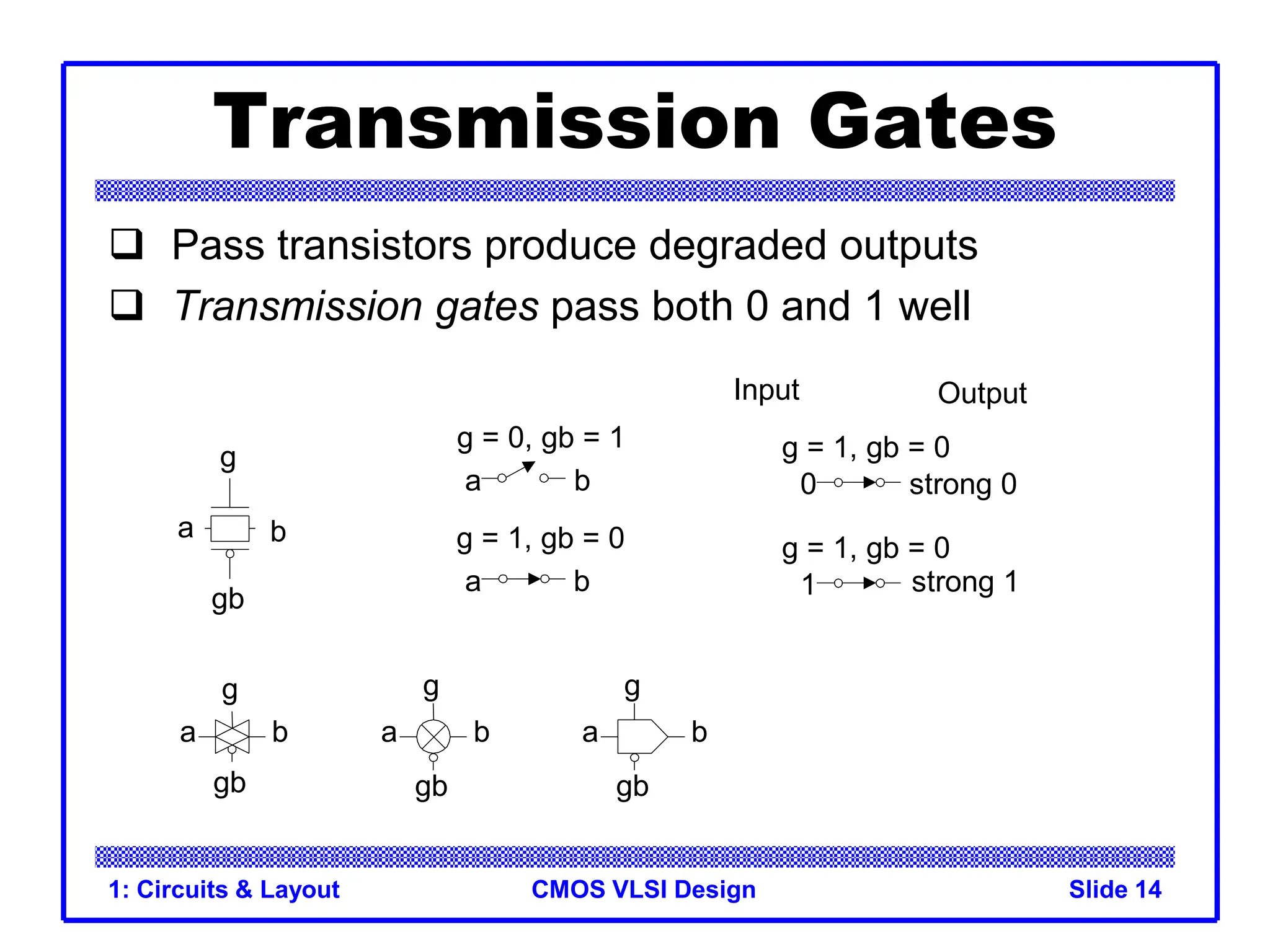
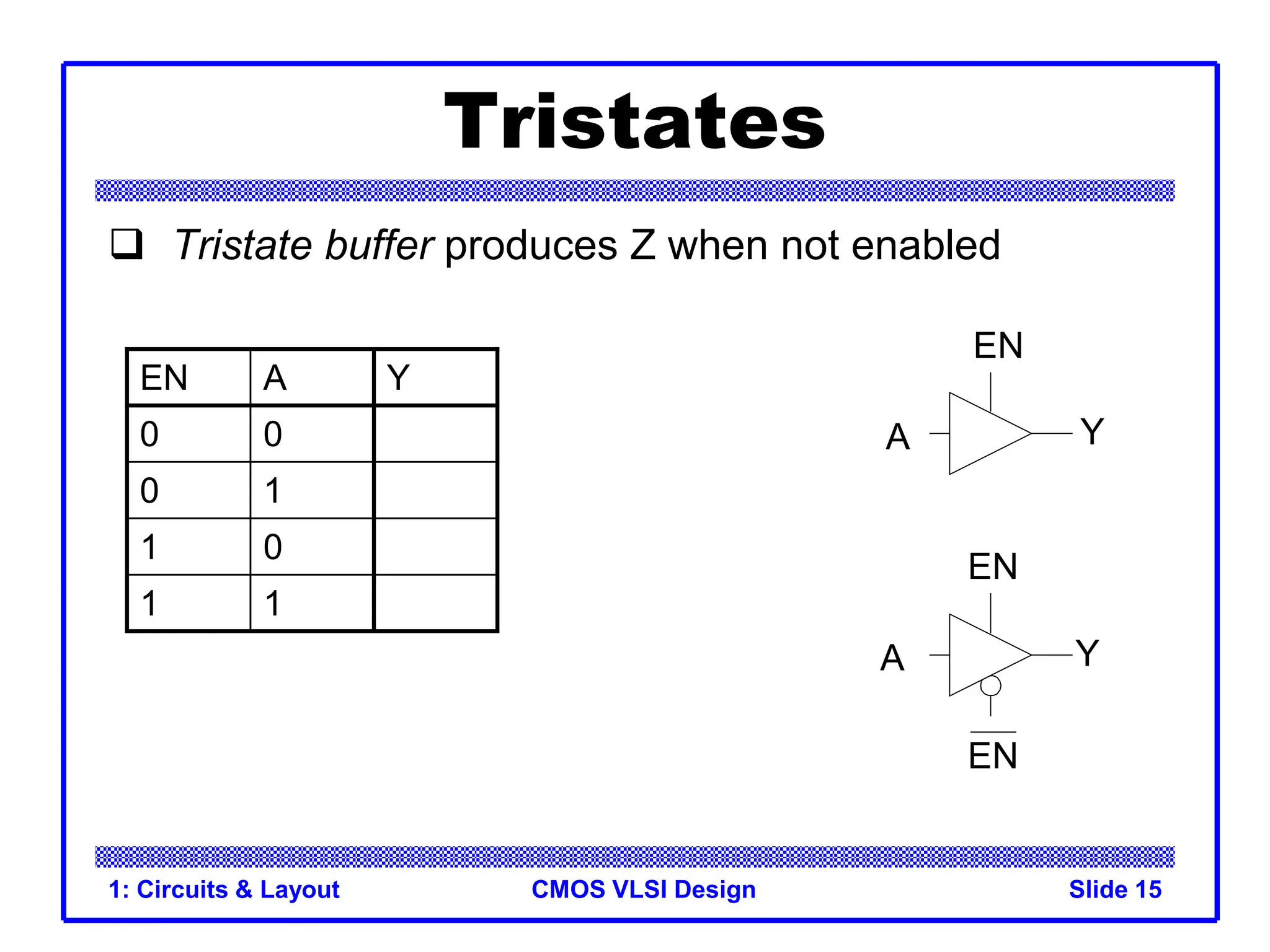
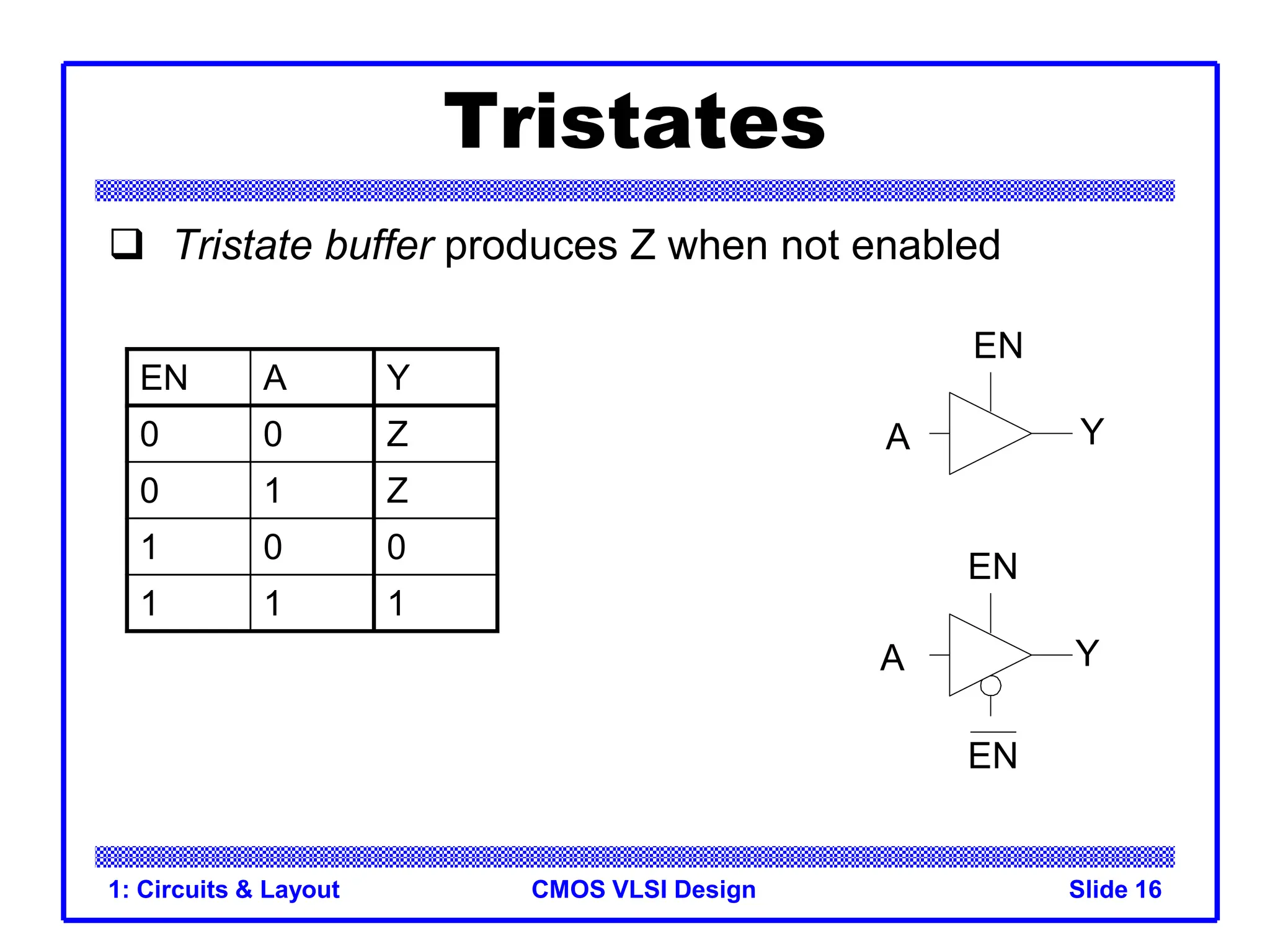
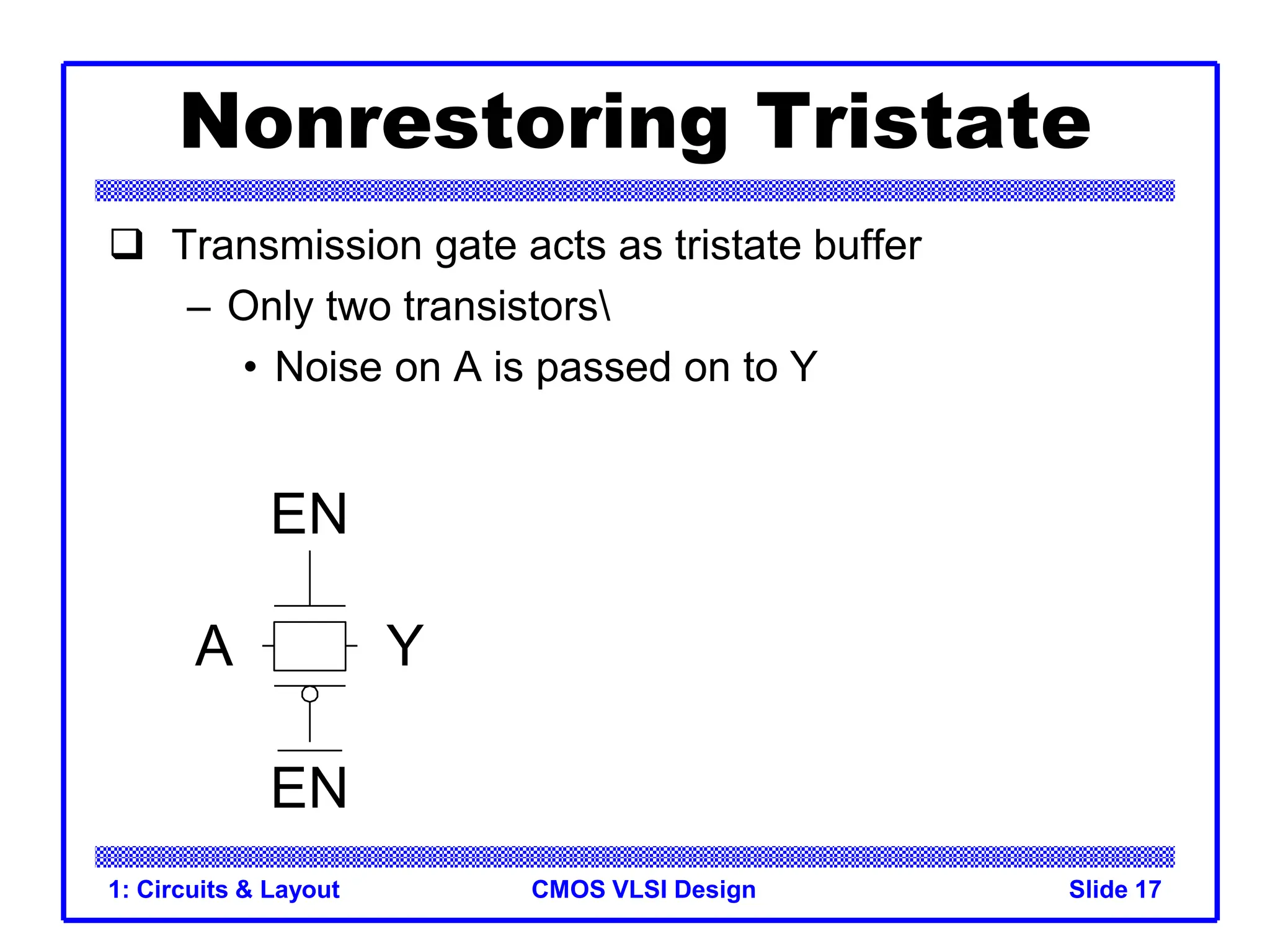
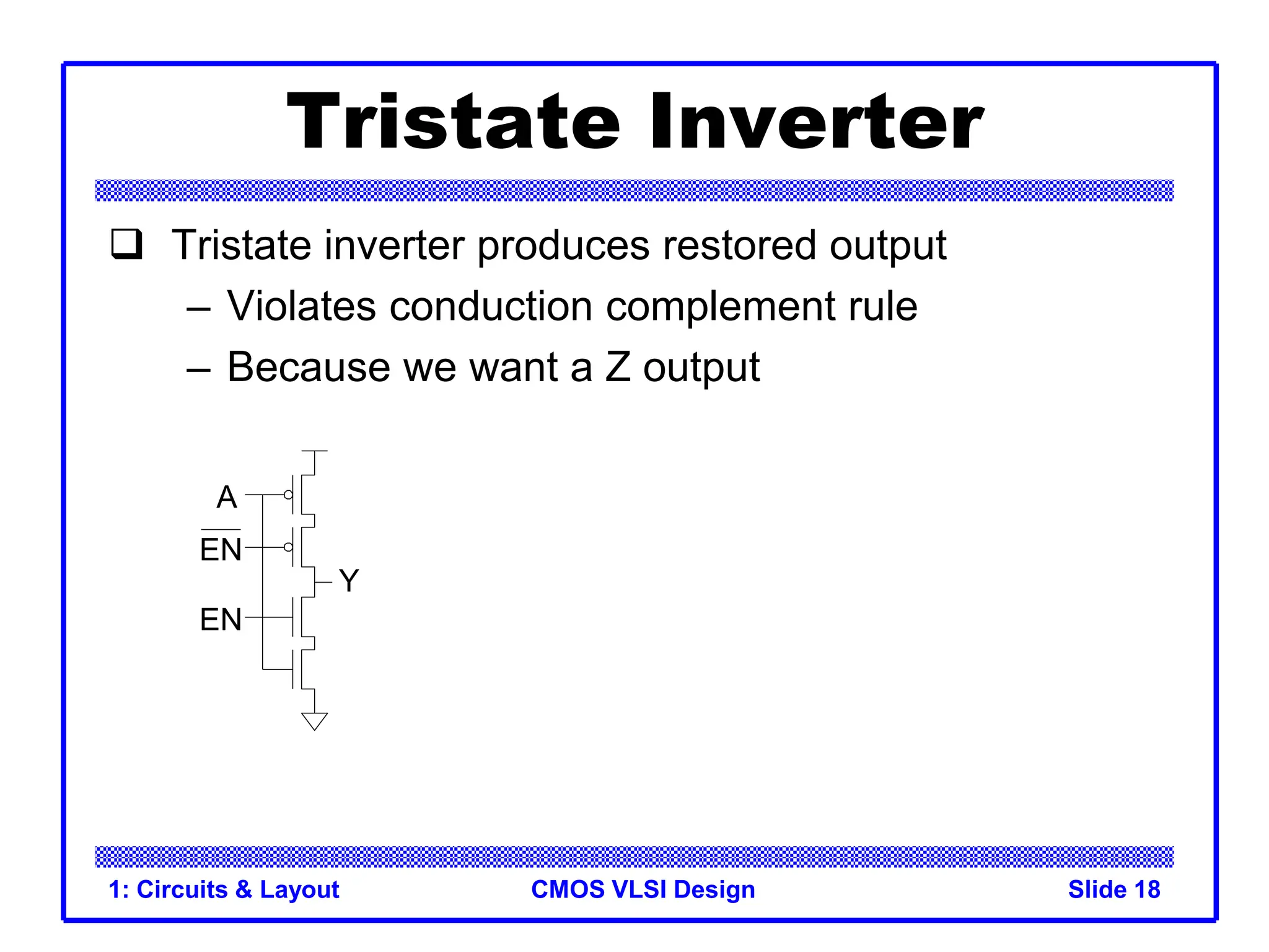
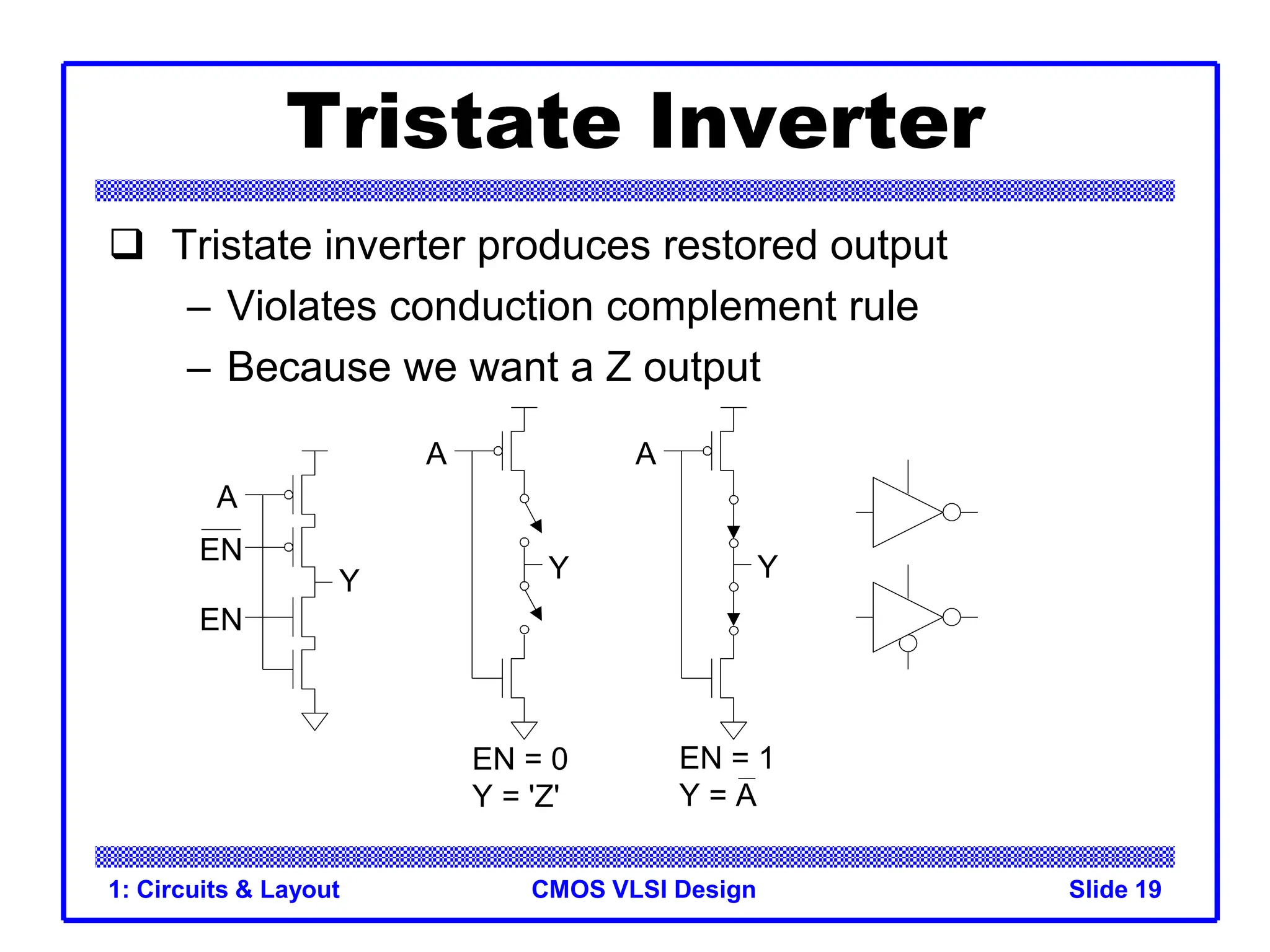
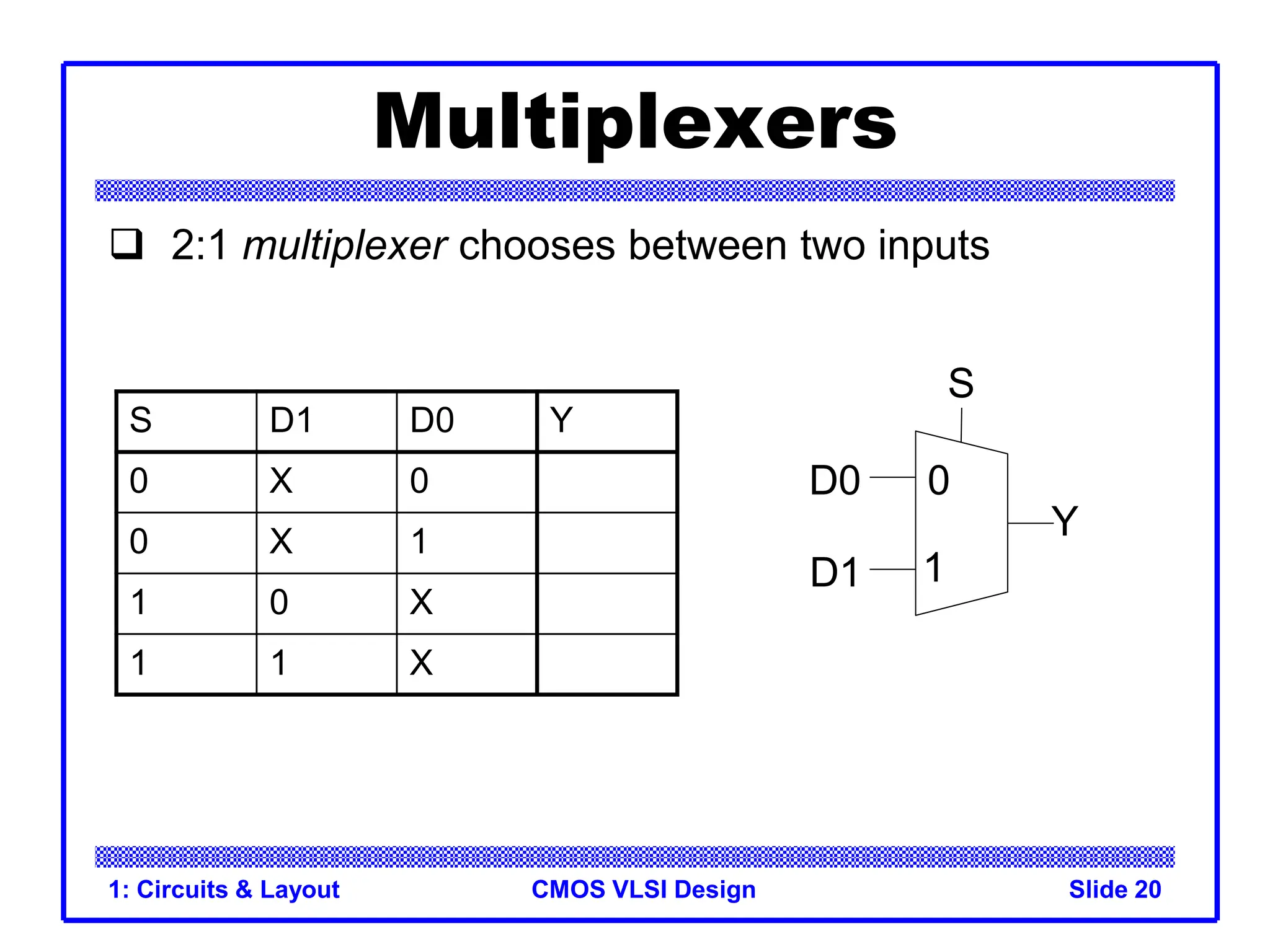
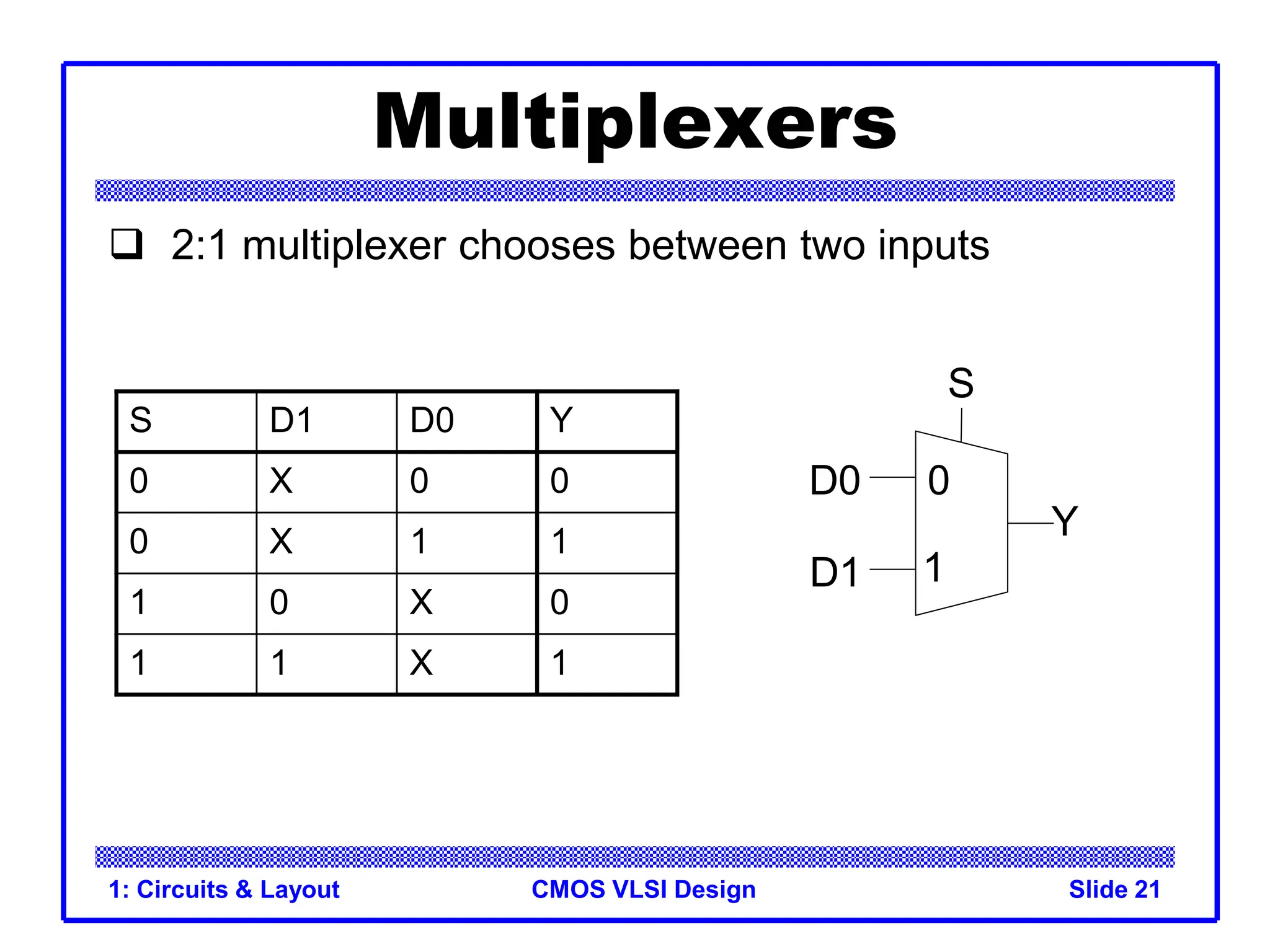
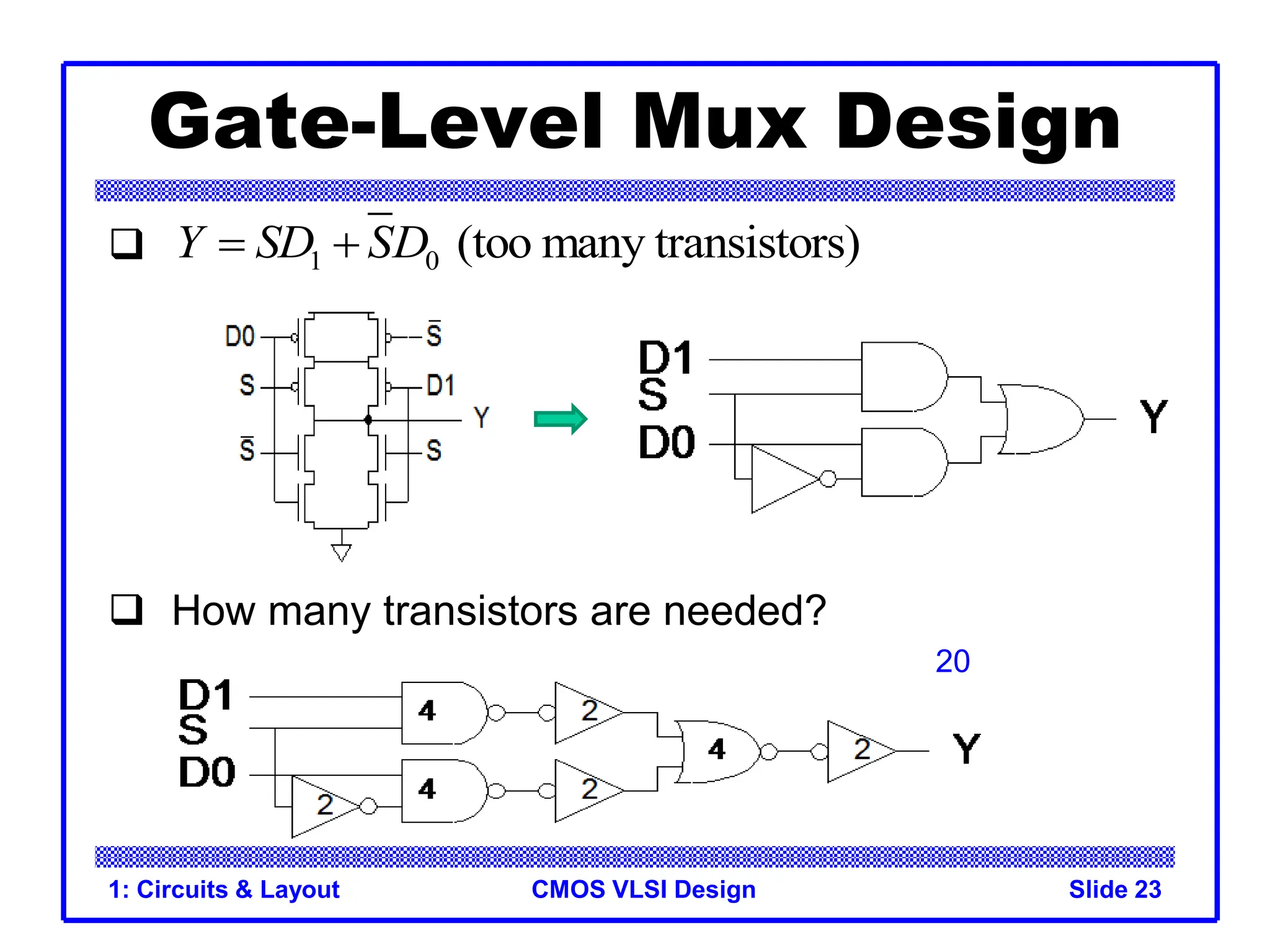
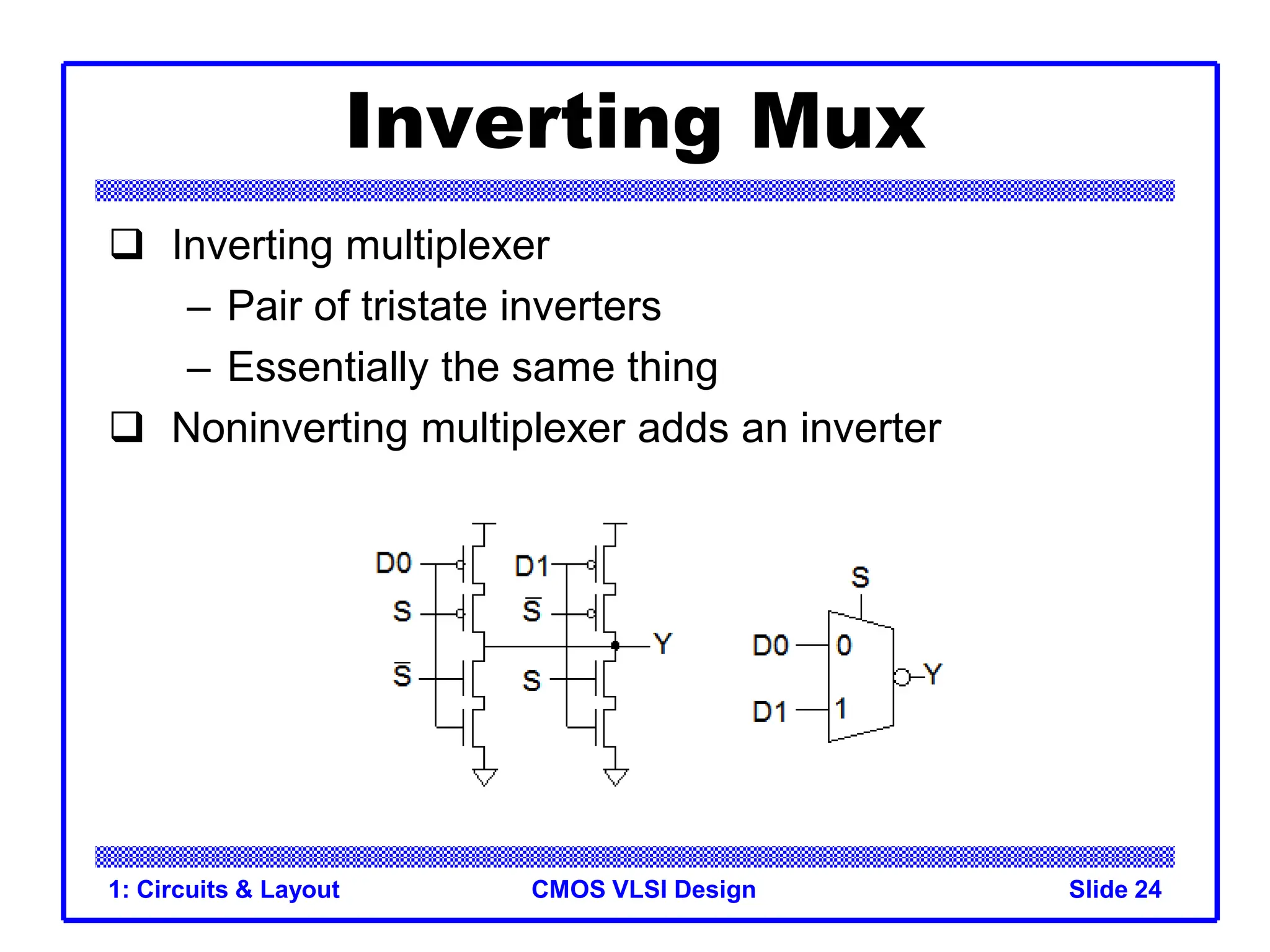
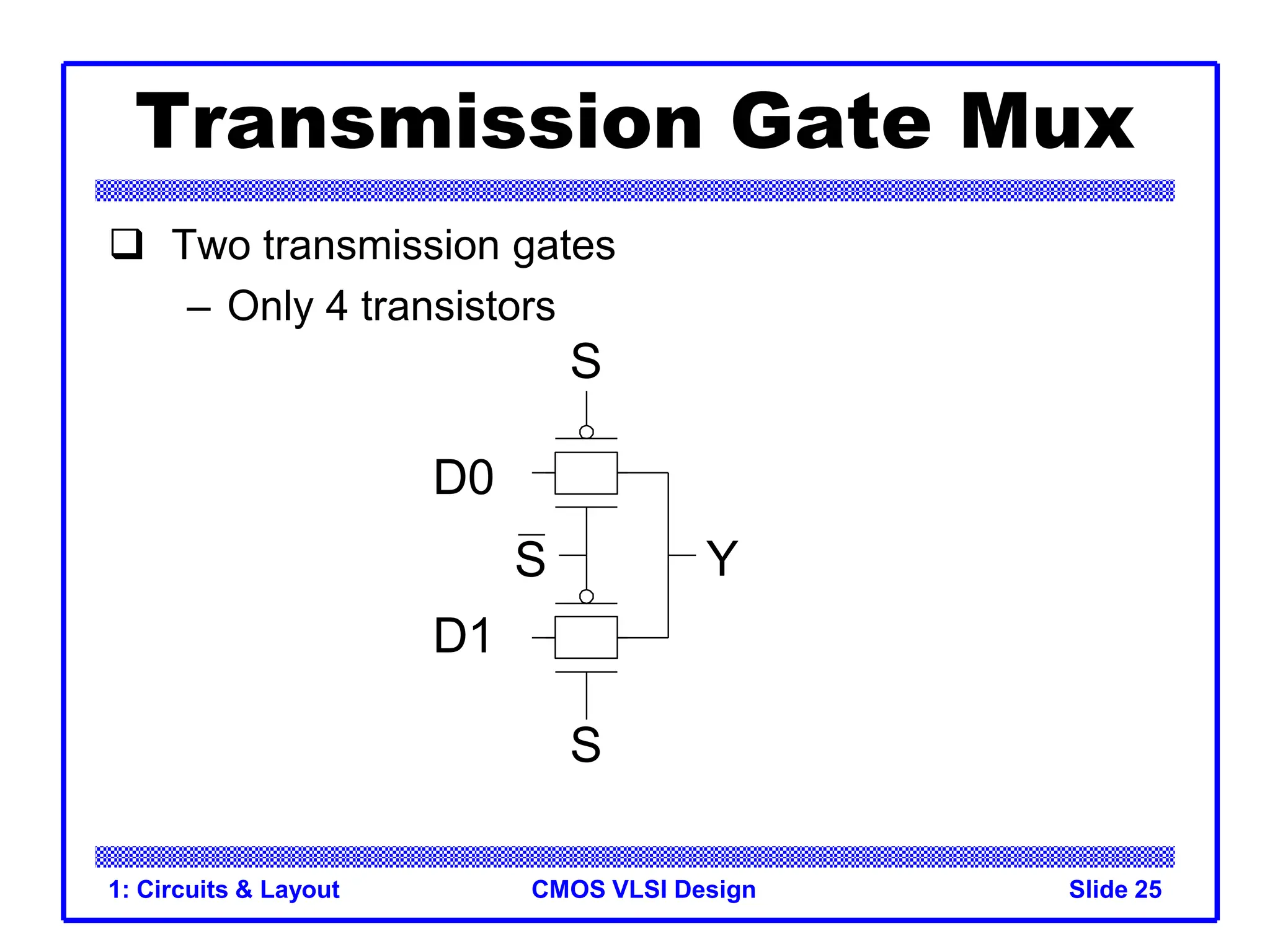
2) The use of pass transistors and transmission gates to implement multiplexers and tristate buffers.
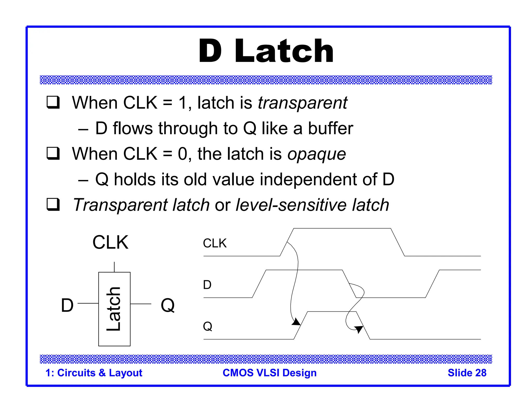
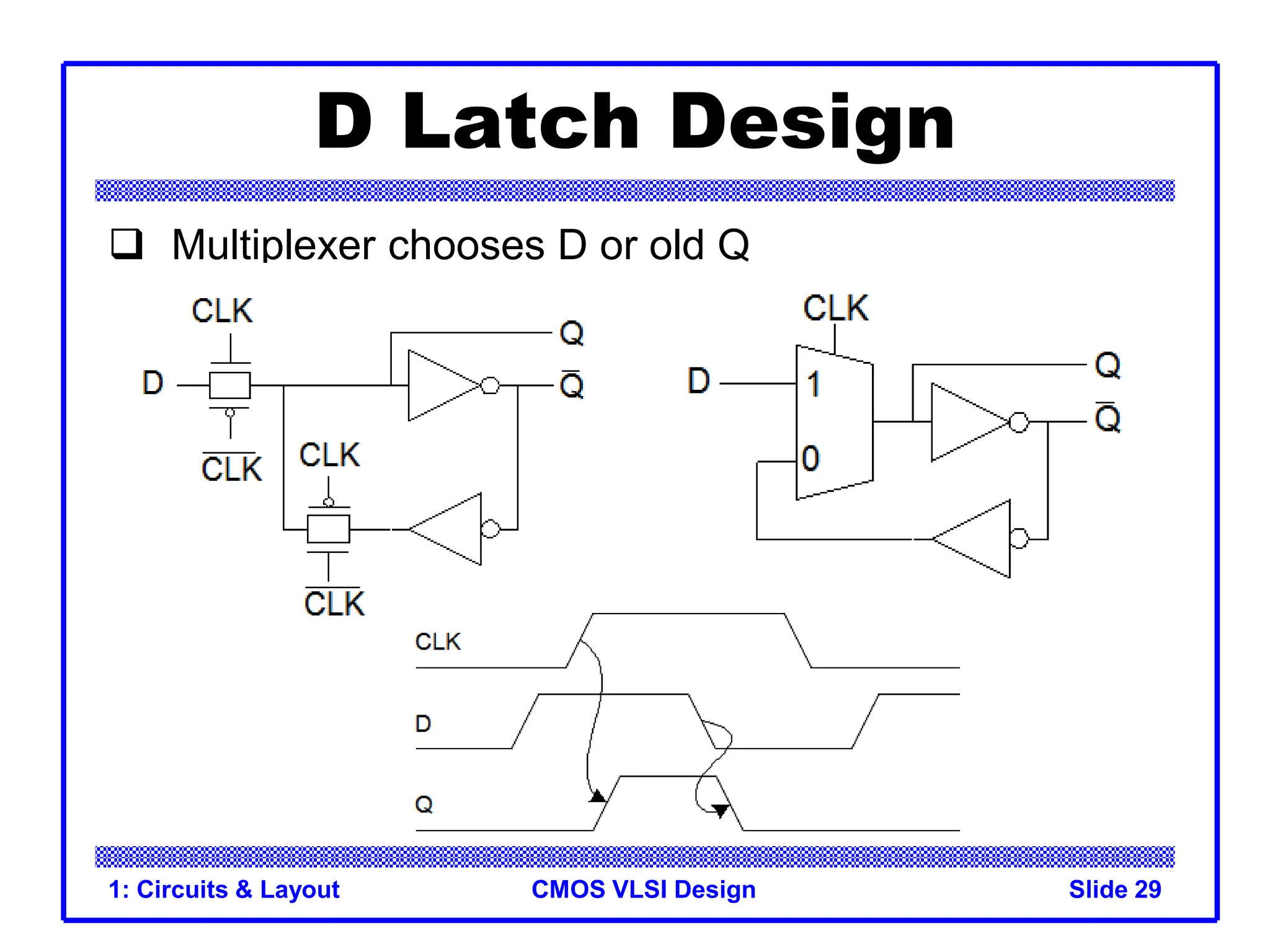
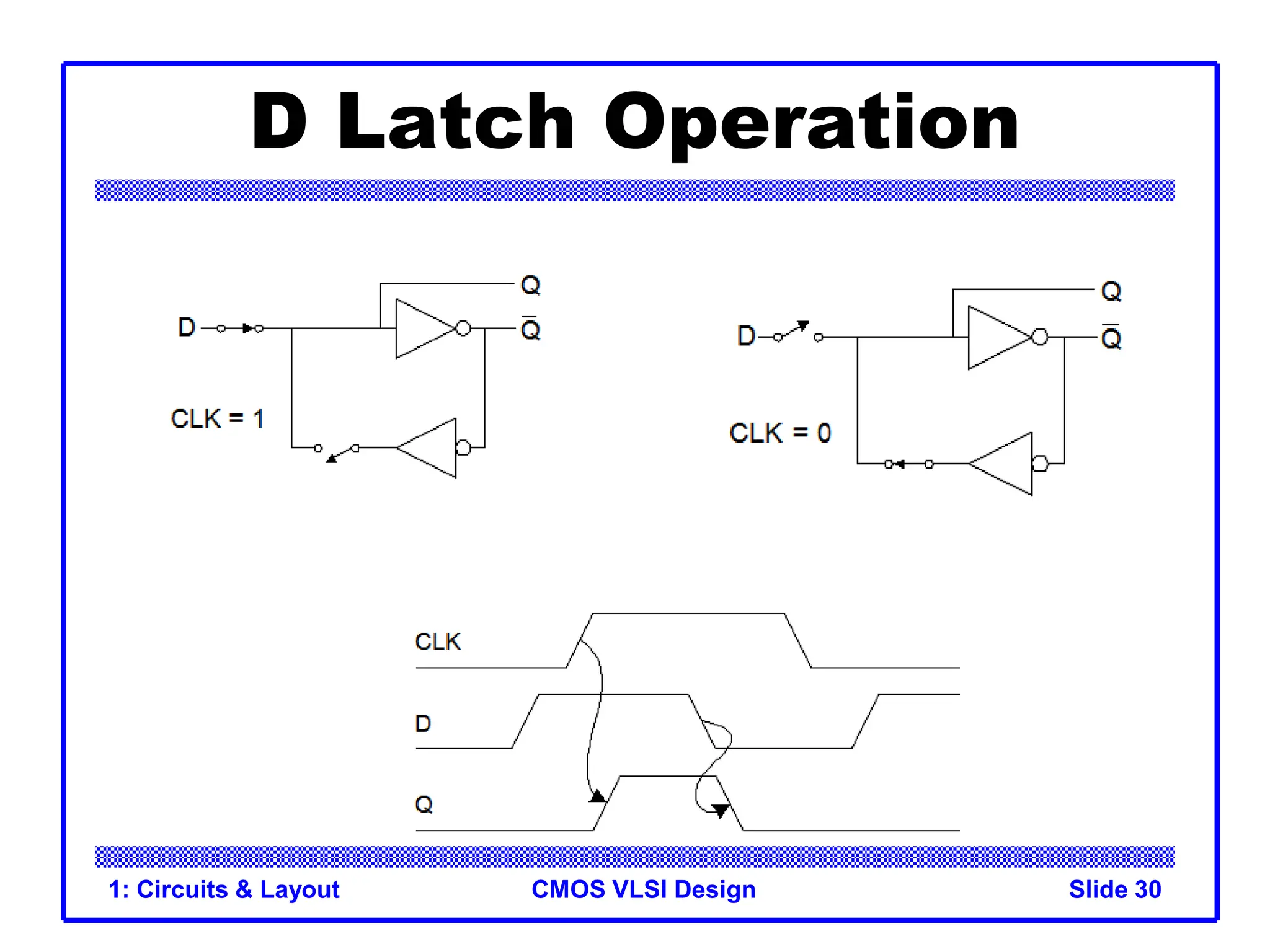
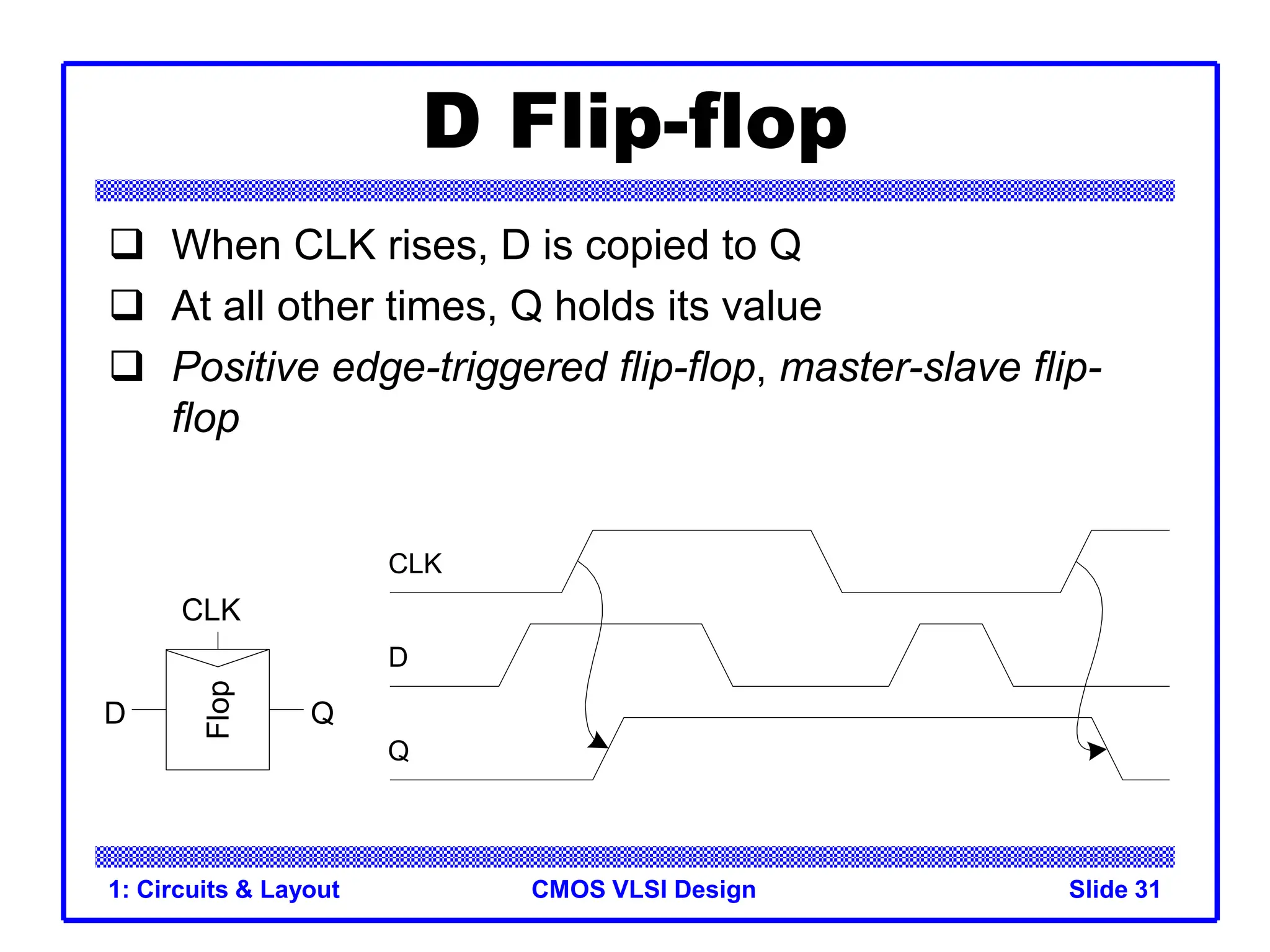
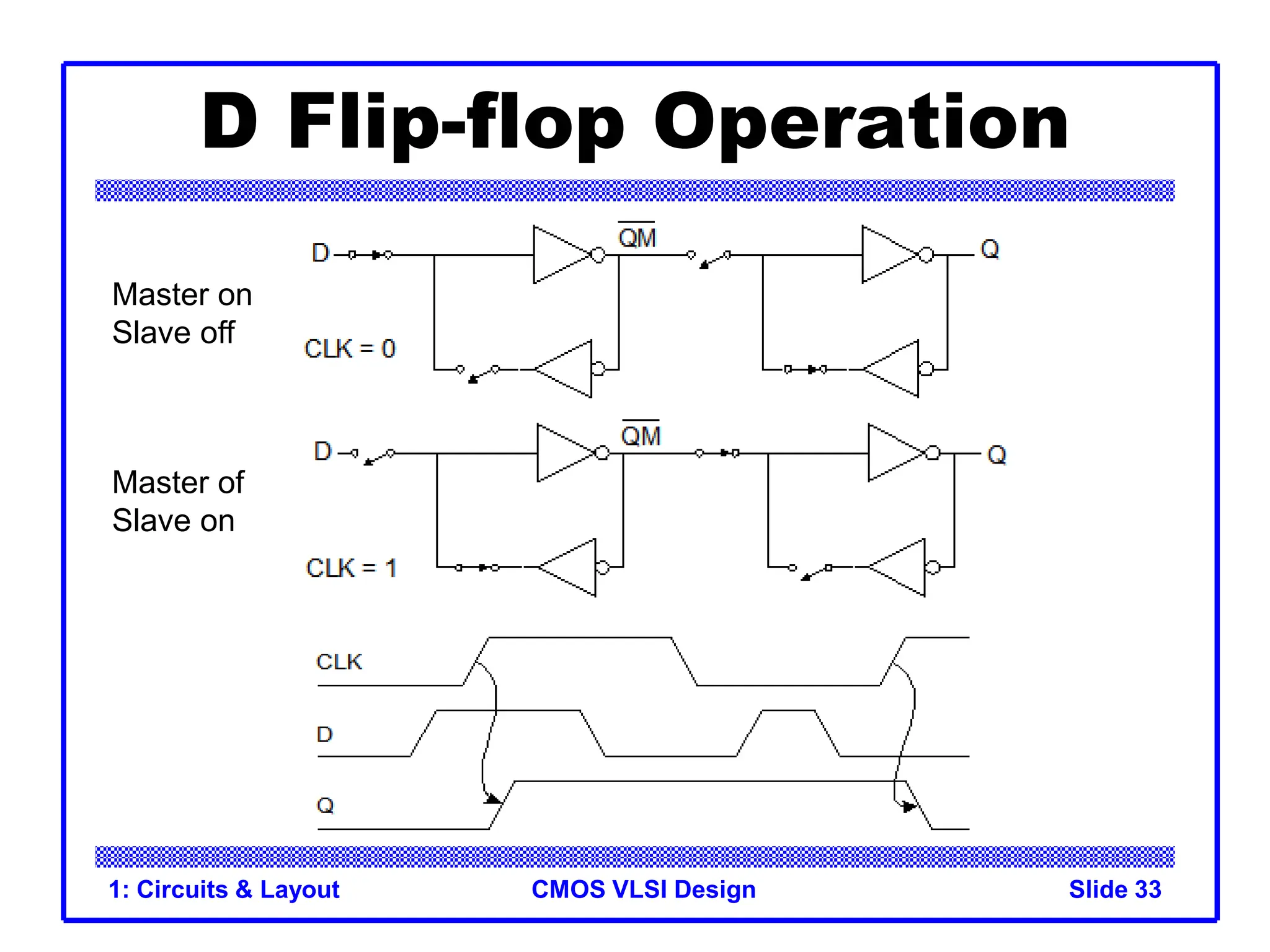
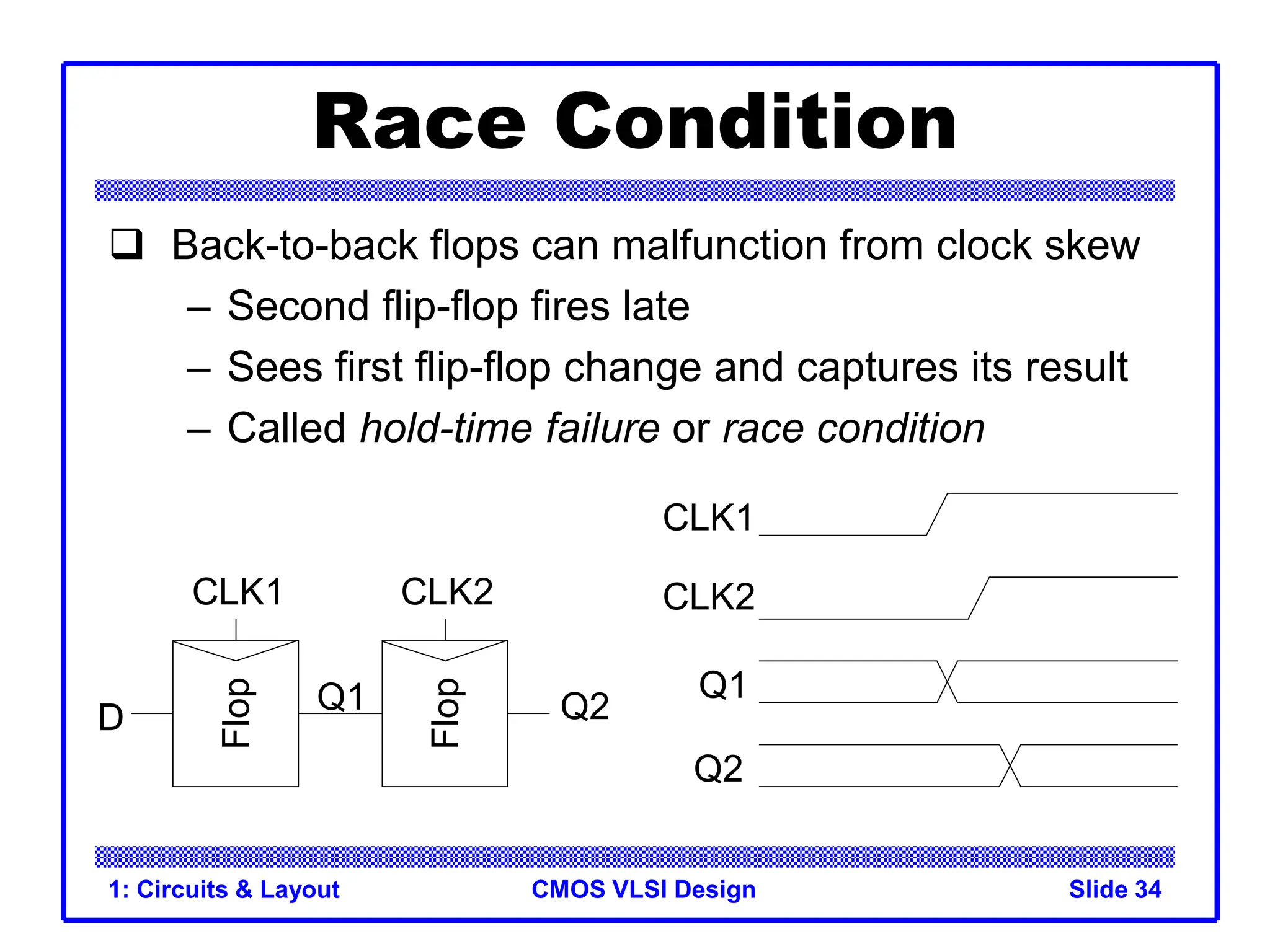
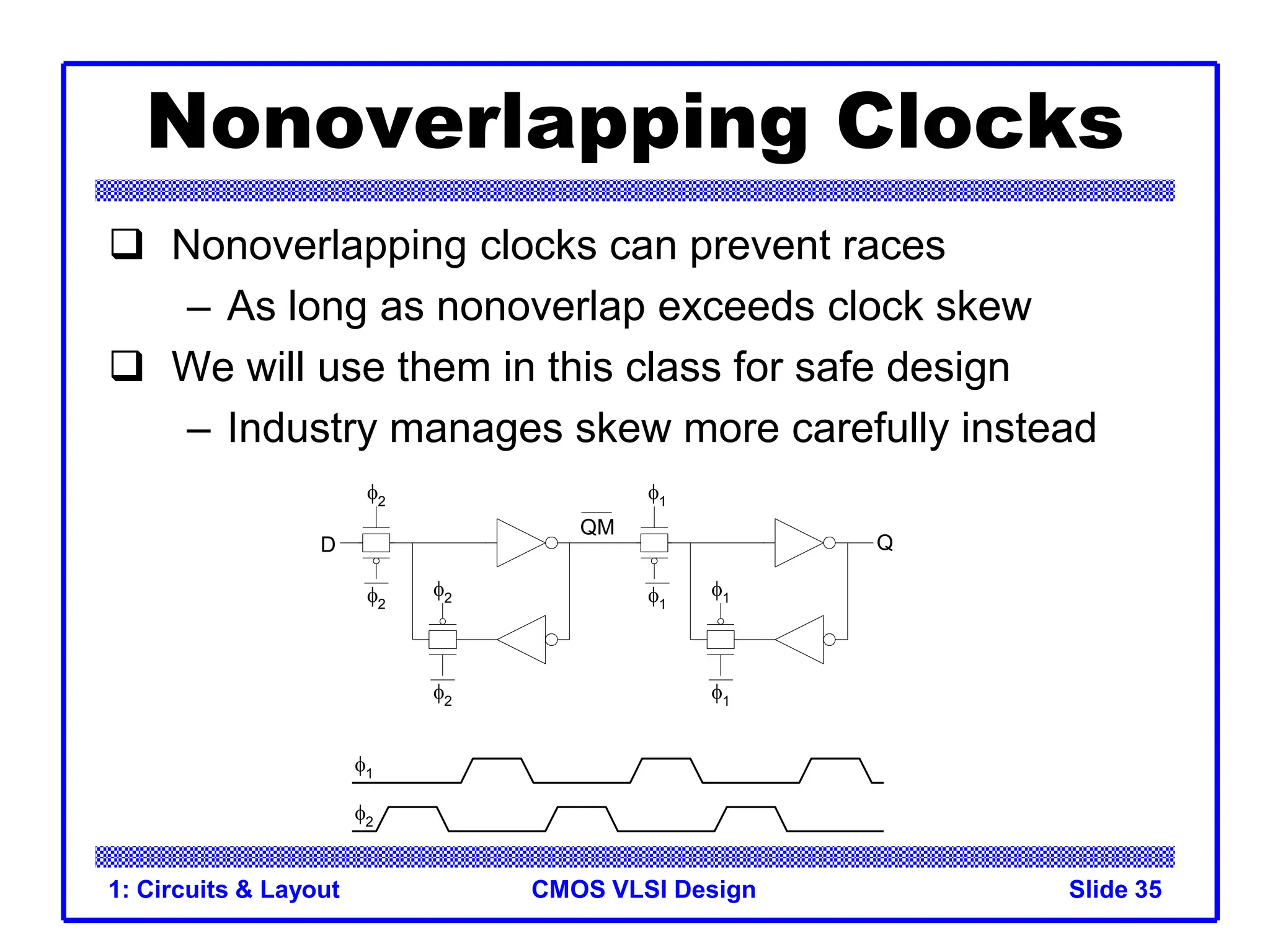
3) The design and operation of basic latches and flip-flops using D latches and a master-slave flip-flop configuration to prevent race conditions between clock signals.


![RF Module Design - [Chapter 4] Transceiver Architecture](https://cdn.slidesharecdn.com/ss_thumbnails/rfch4-150613070346-lva1-app6891-thumbnail.jpg?width=640&height=640&fit=bounds)