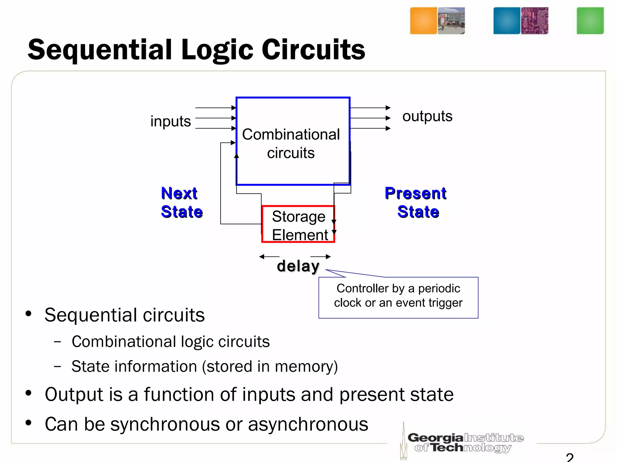
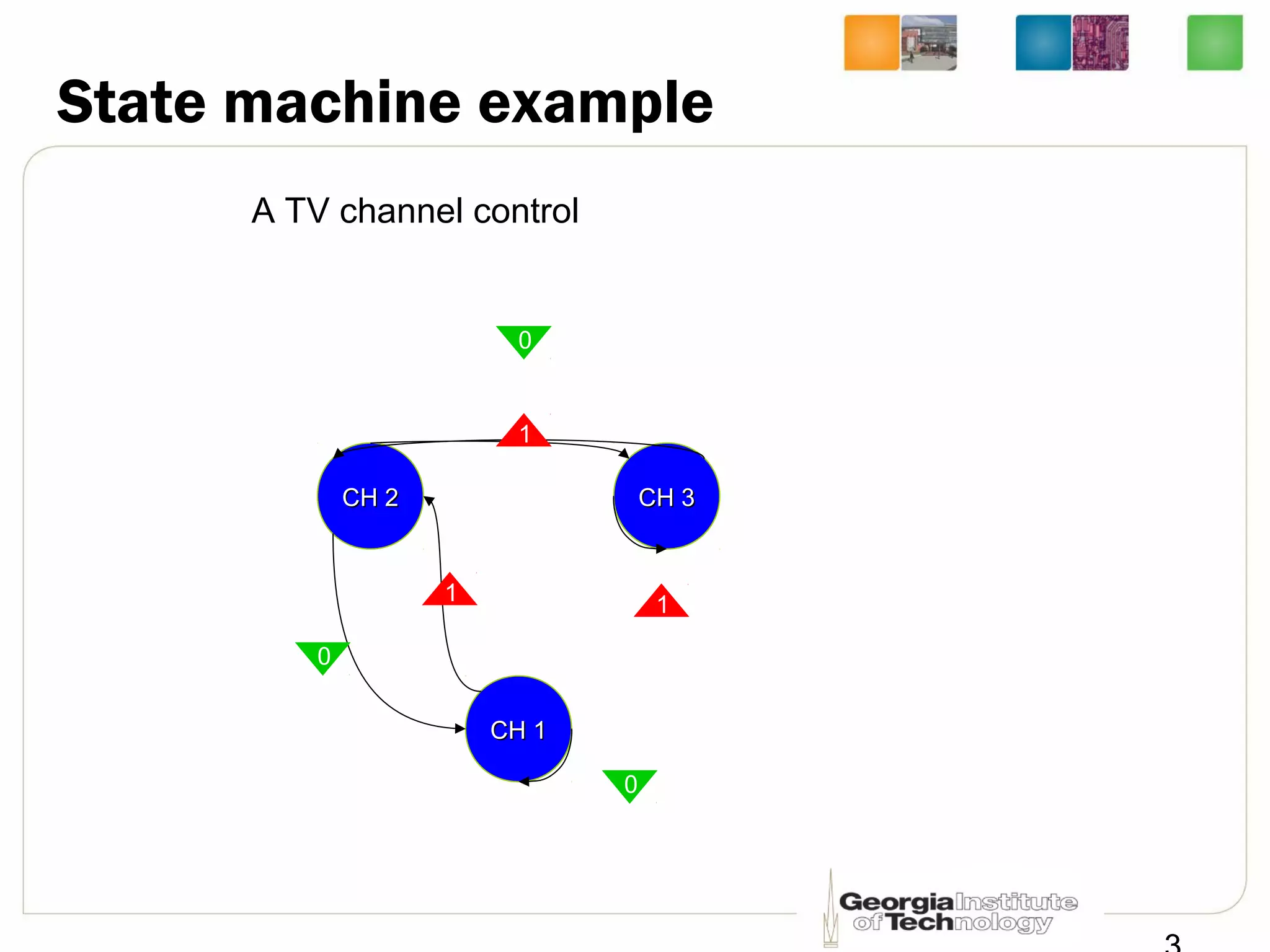
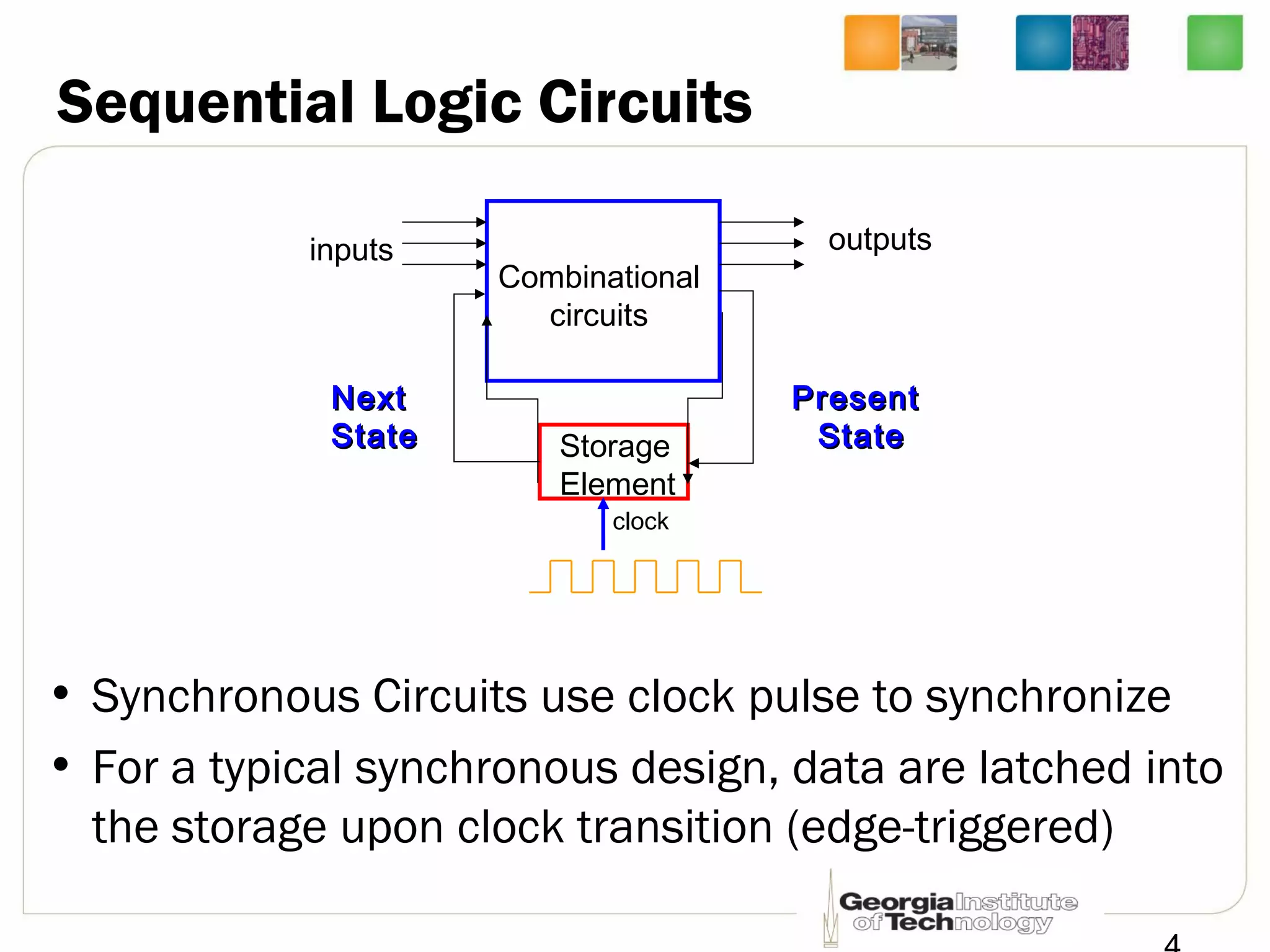
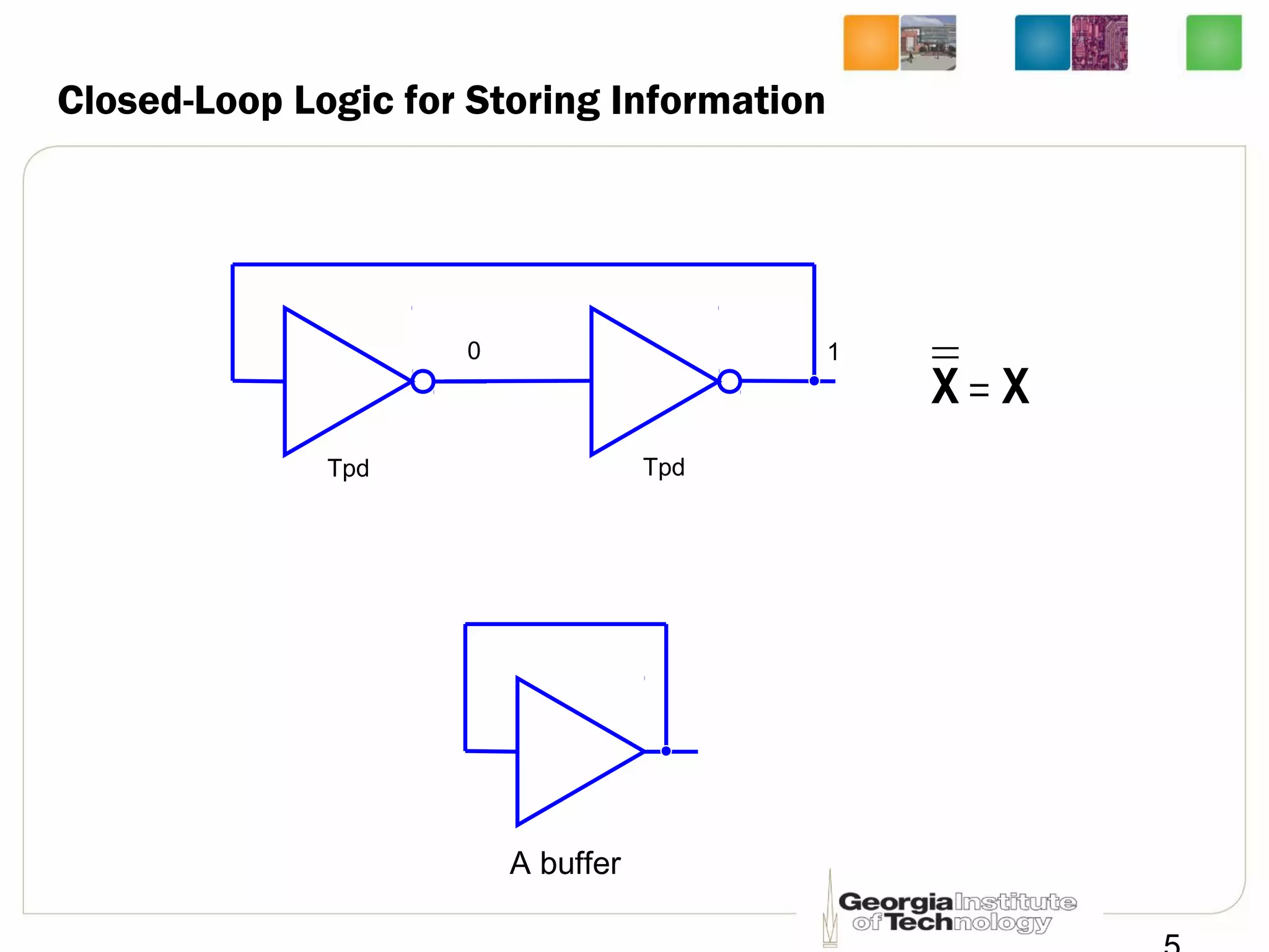
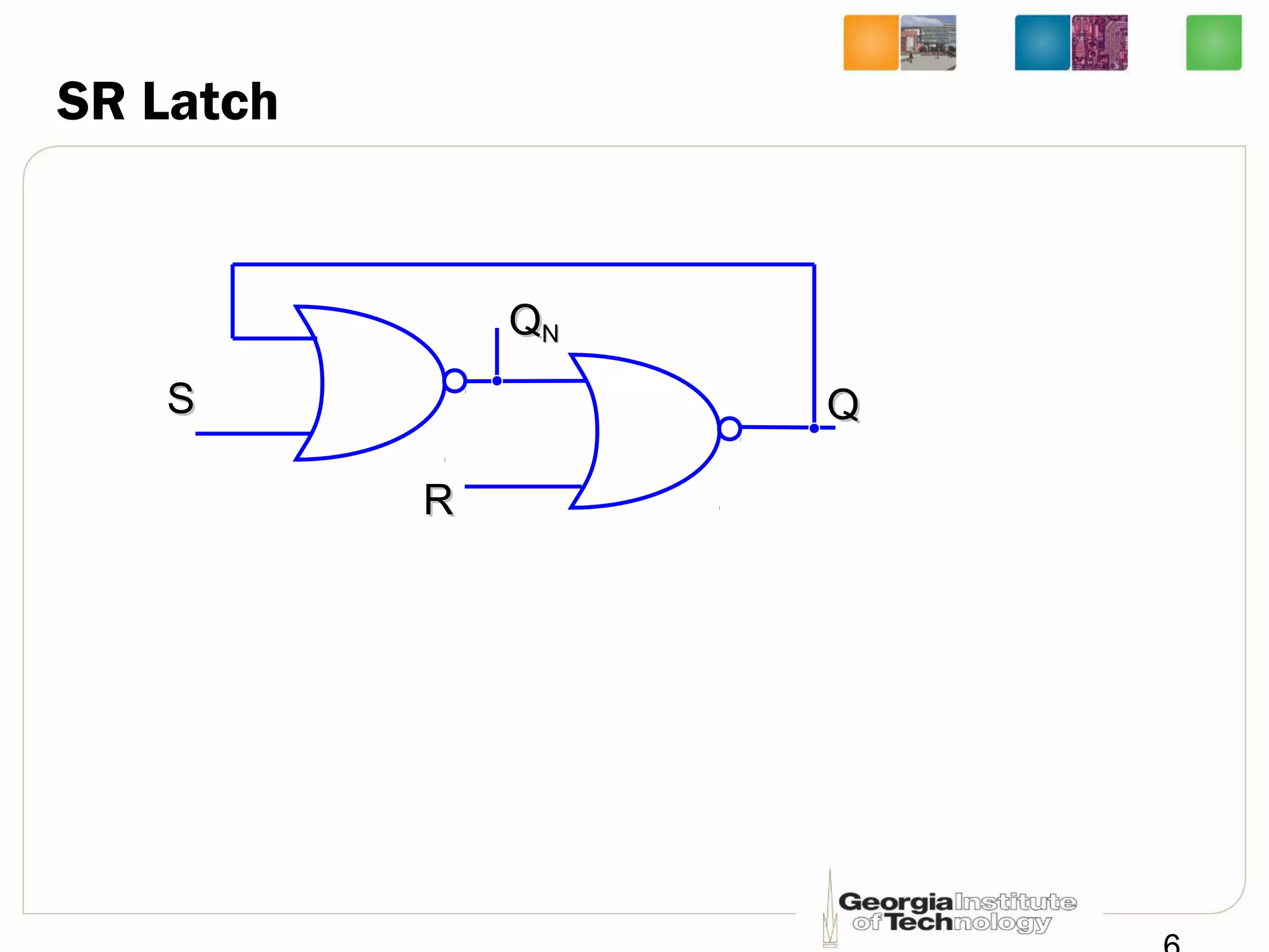
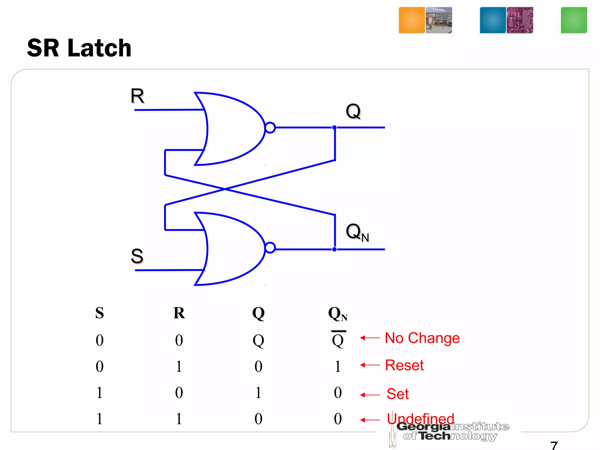
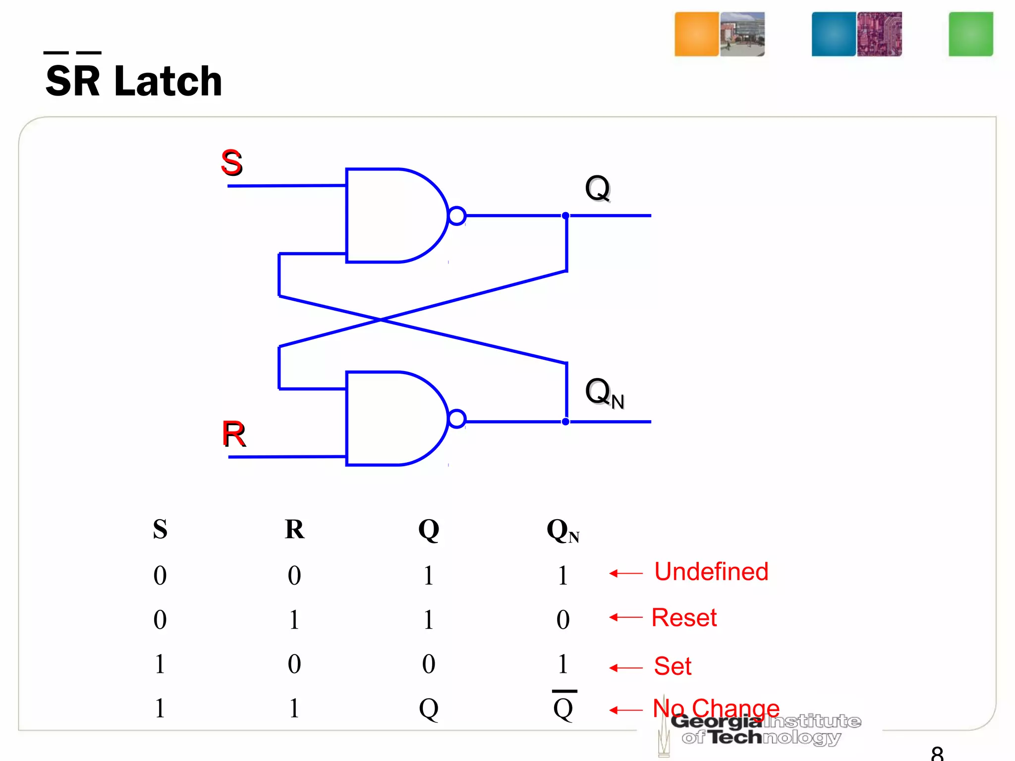
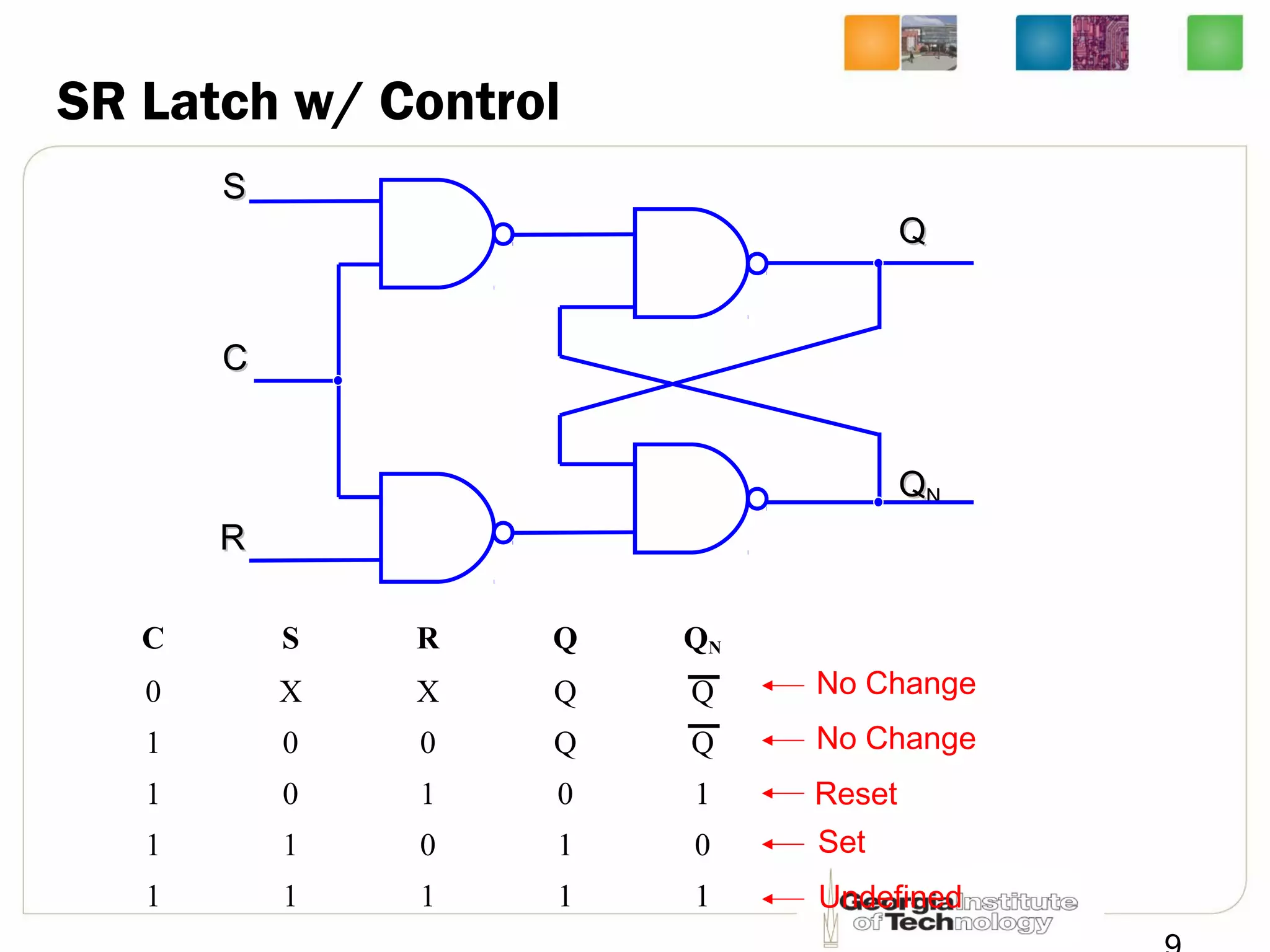
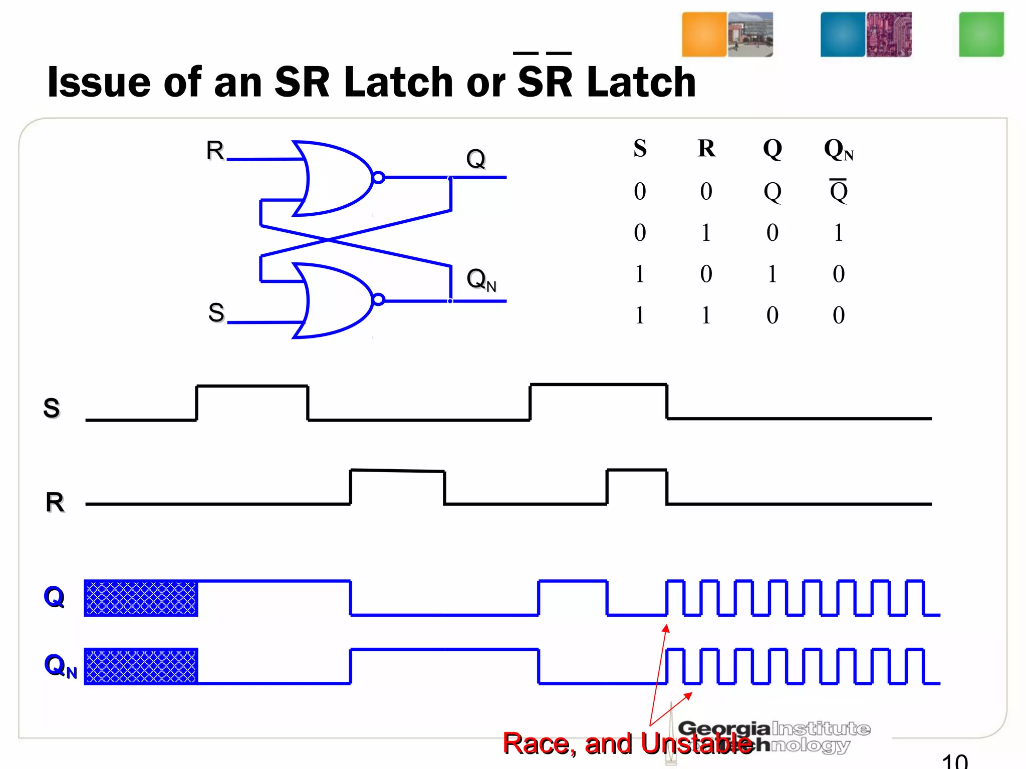
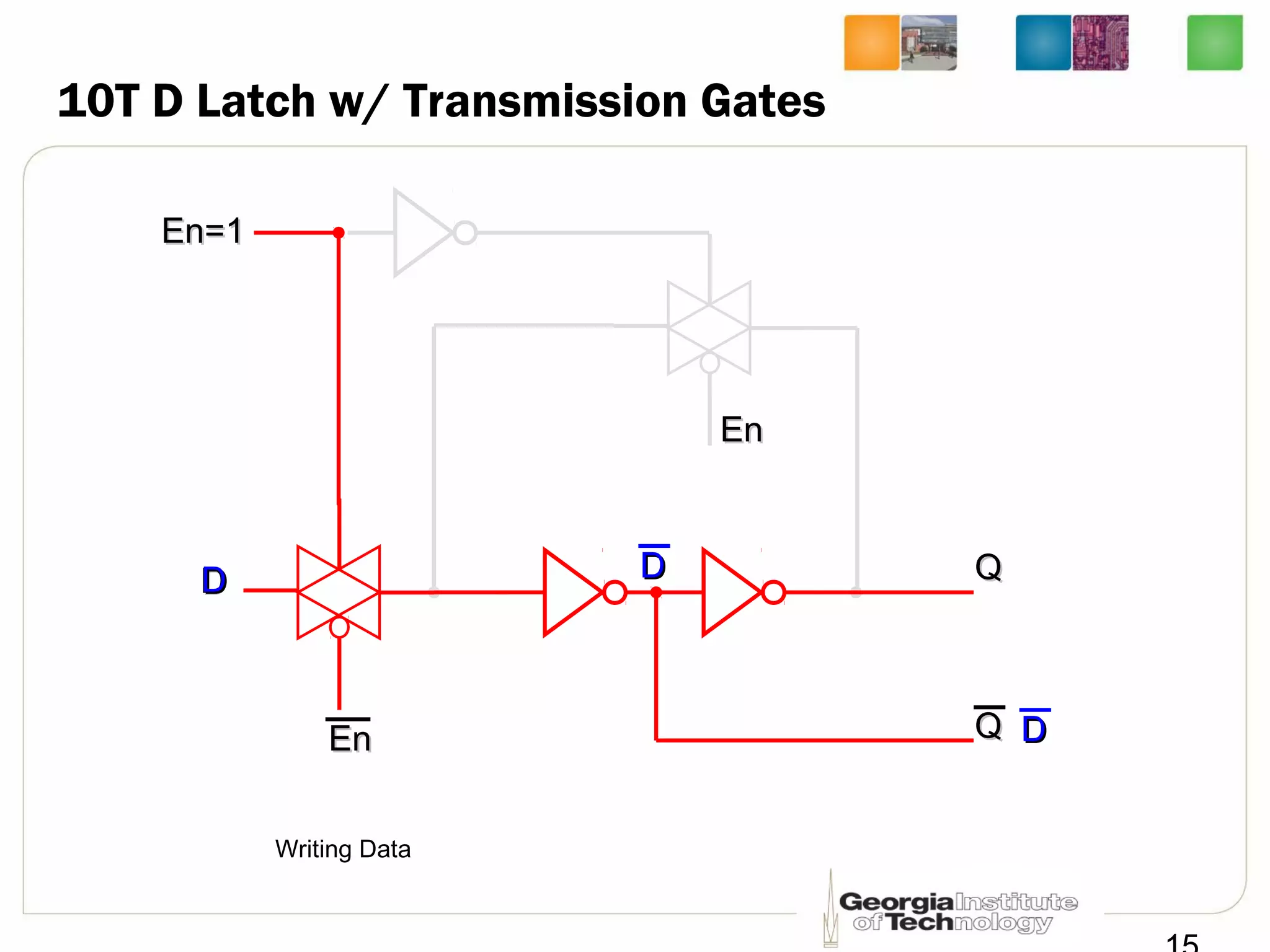
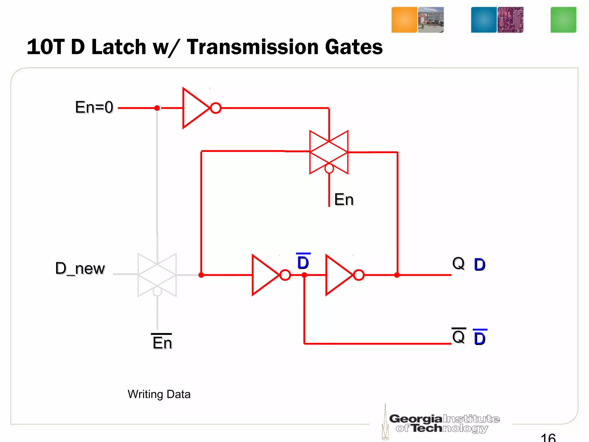
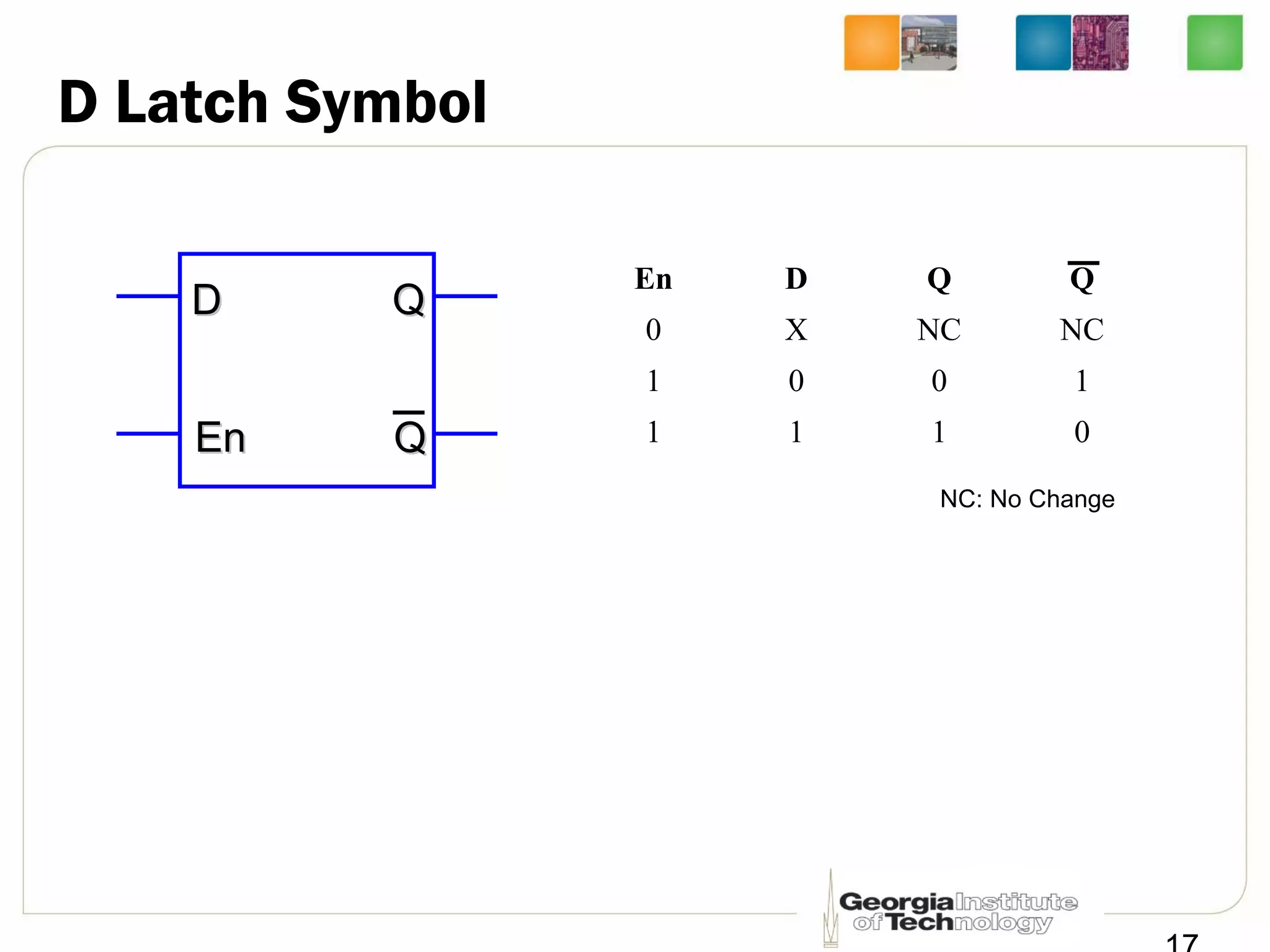
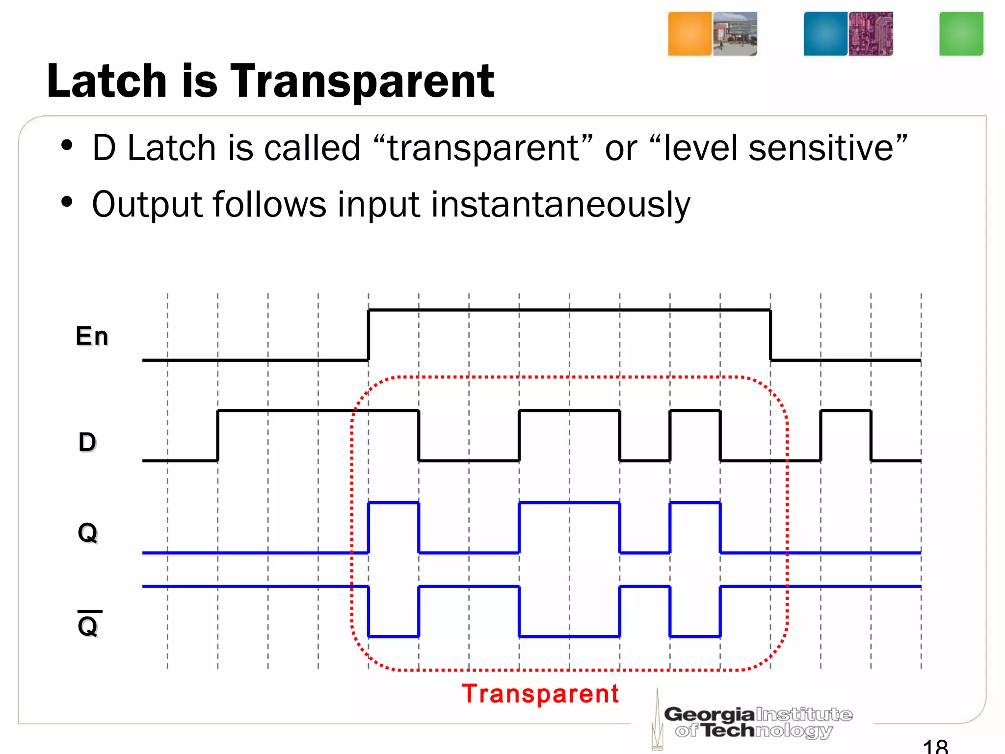
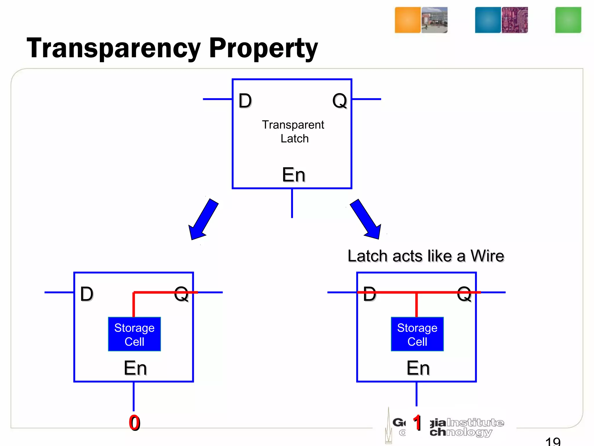
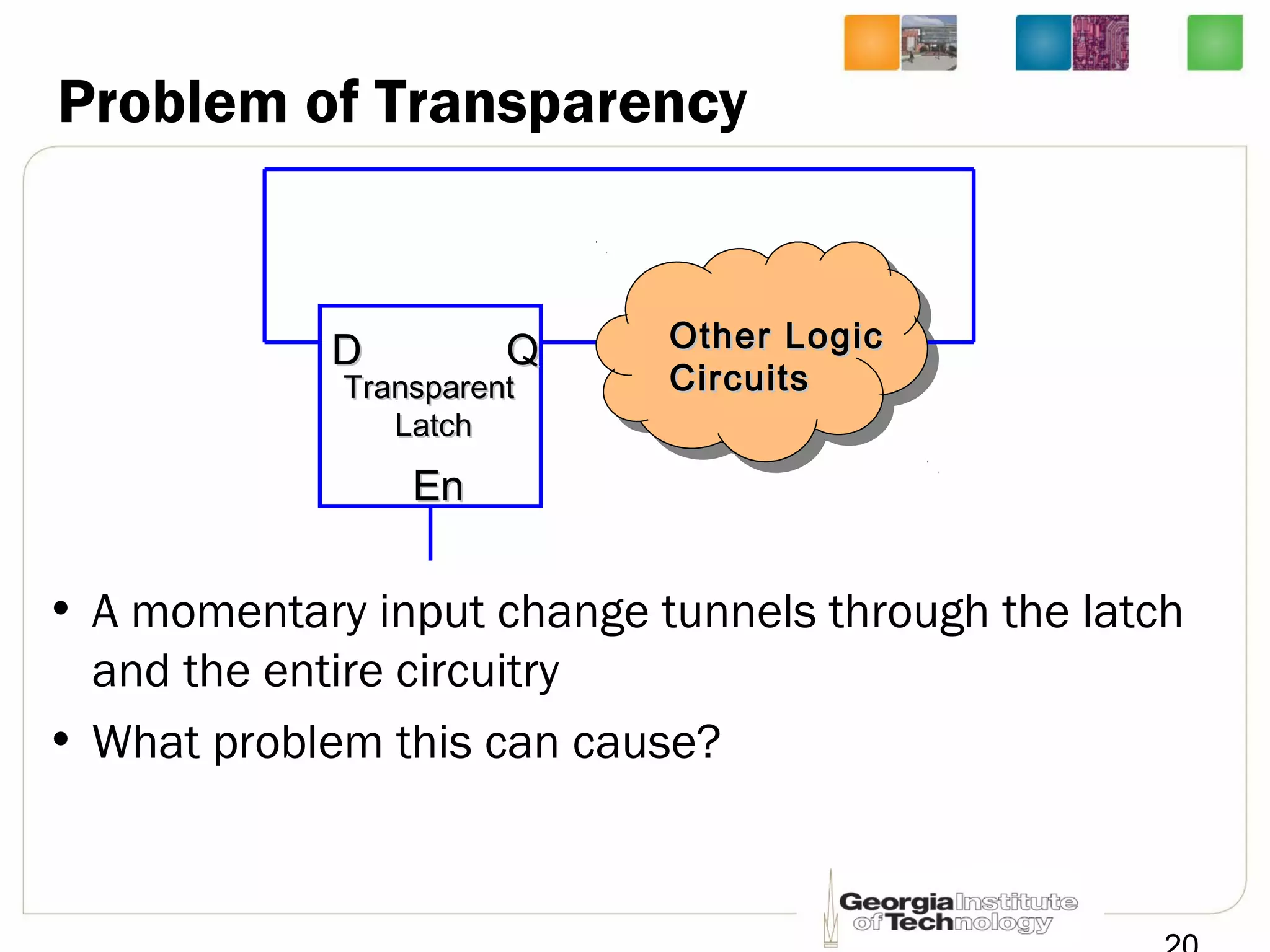
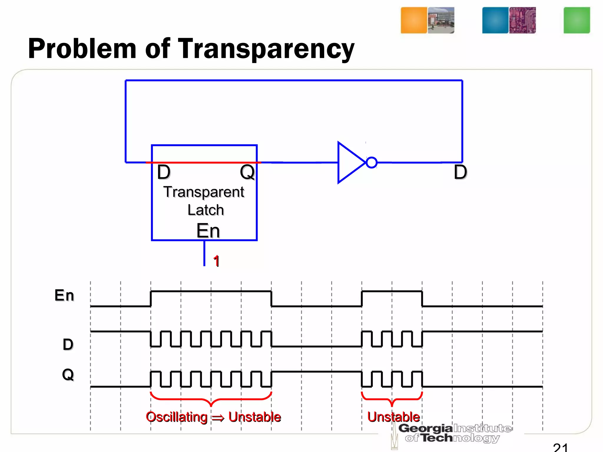
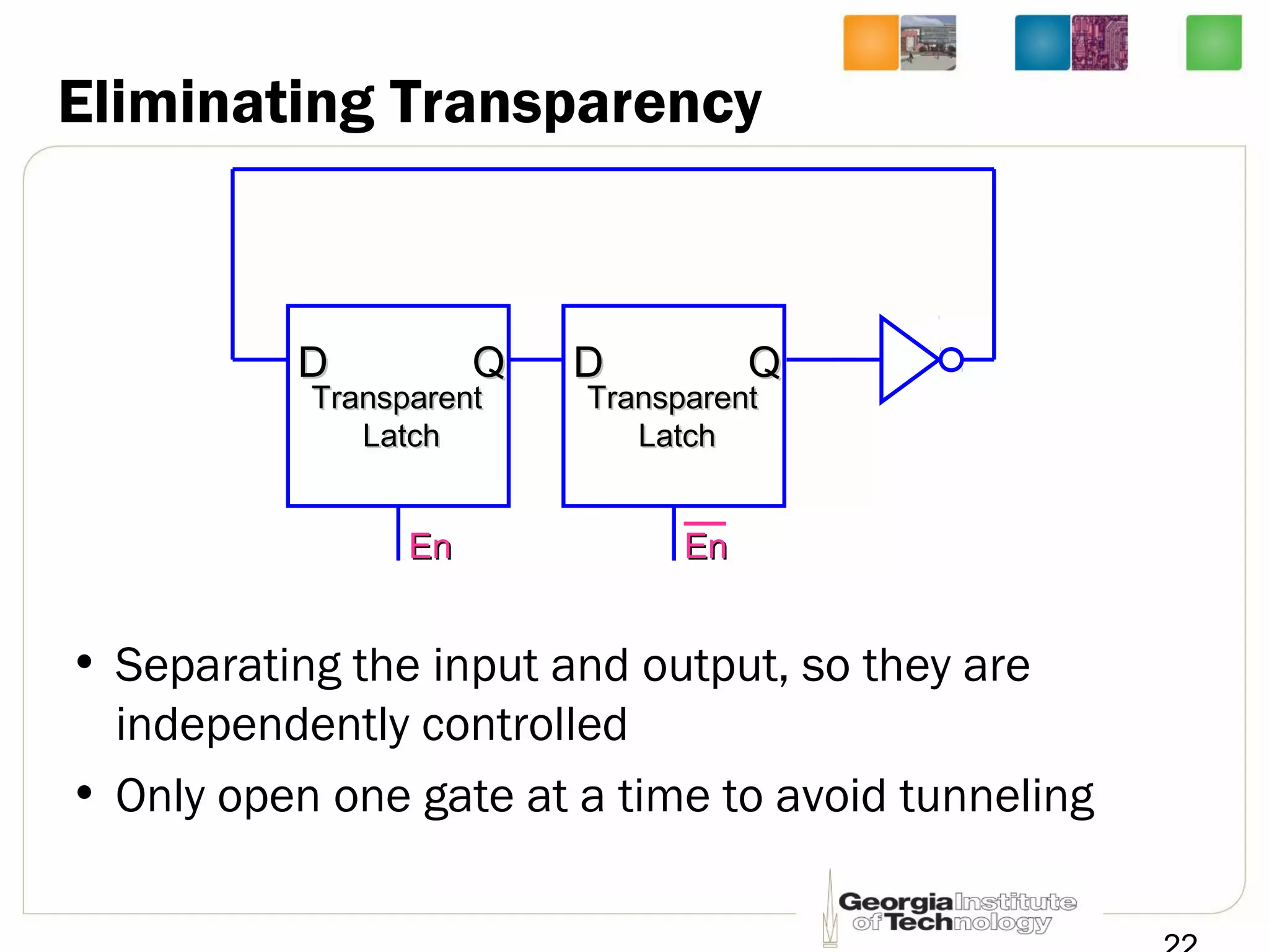
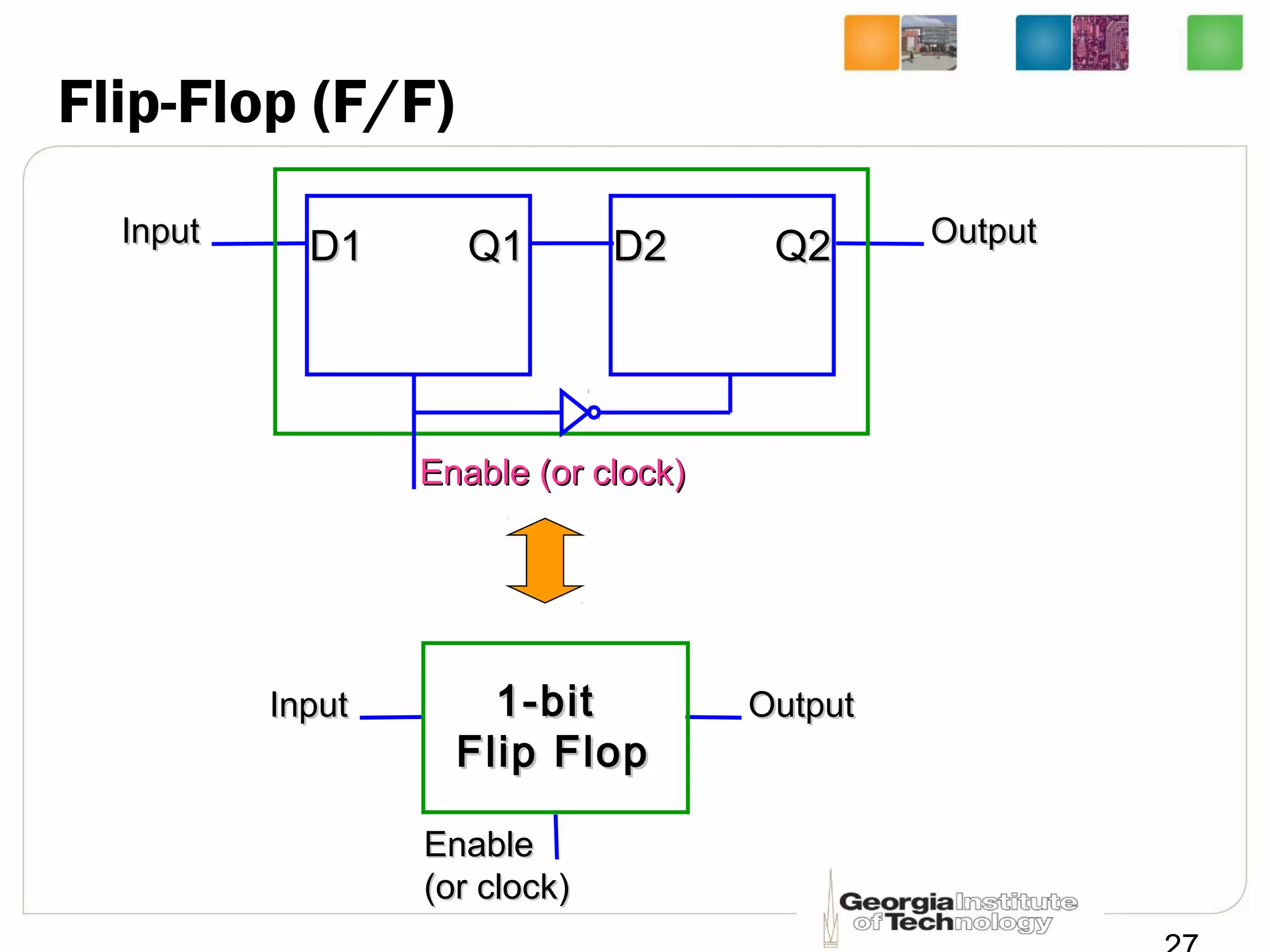
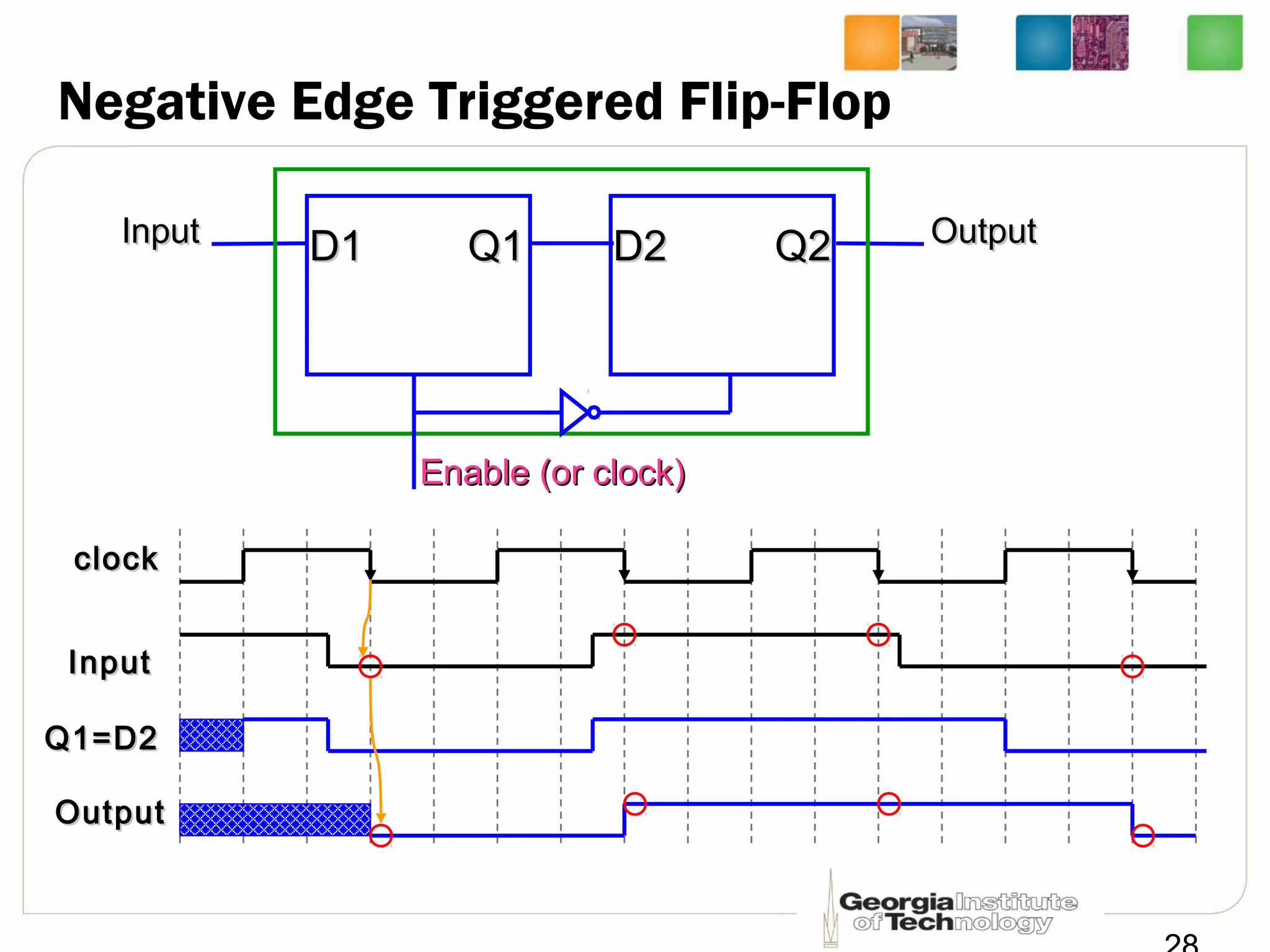
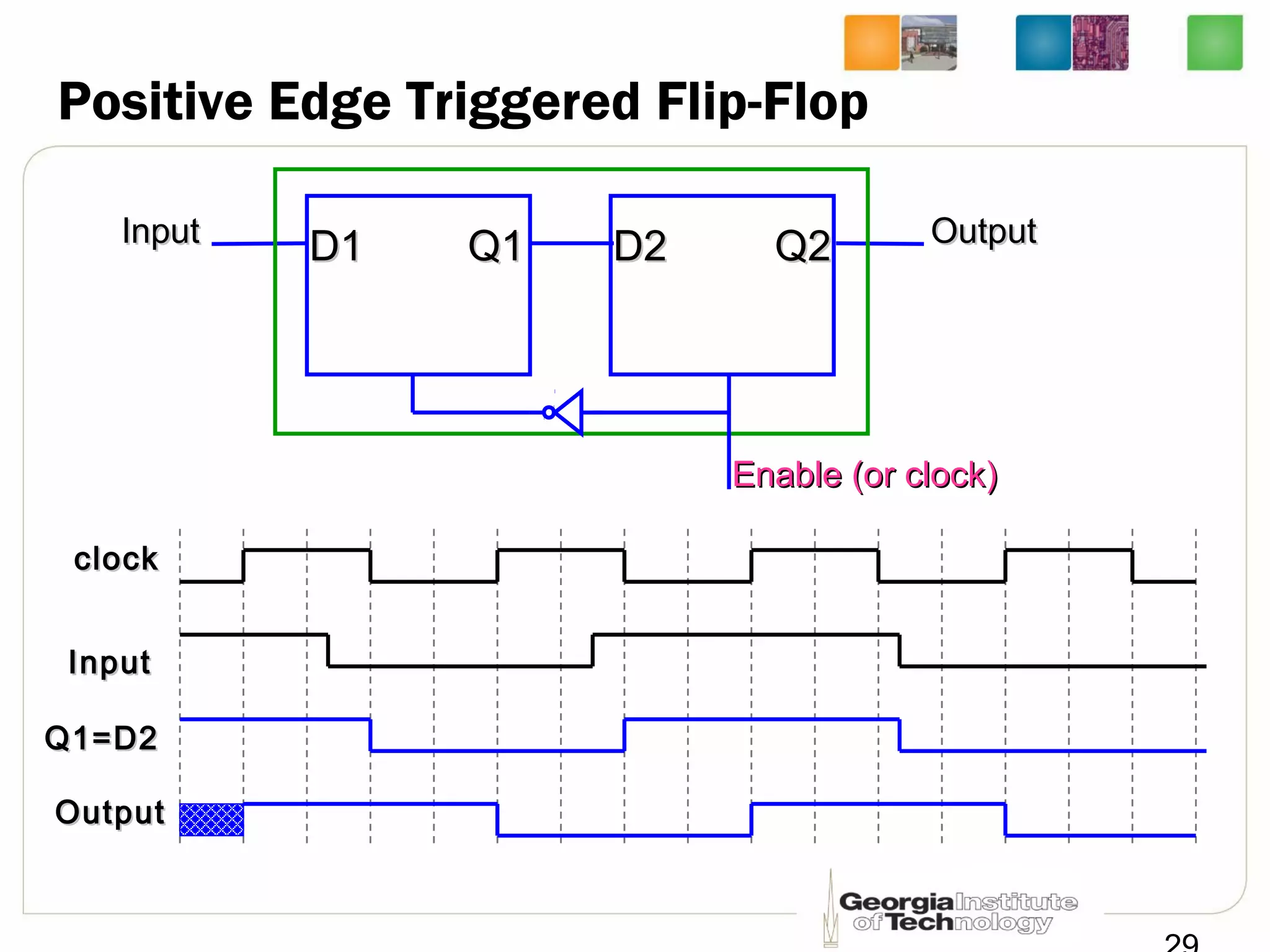
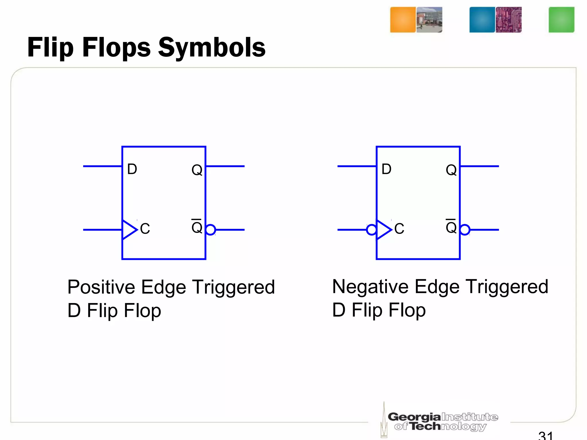
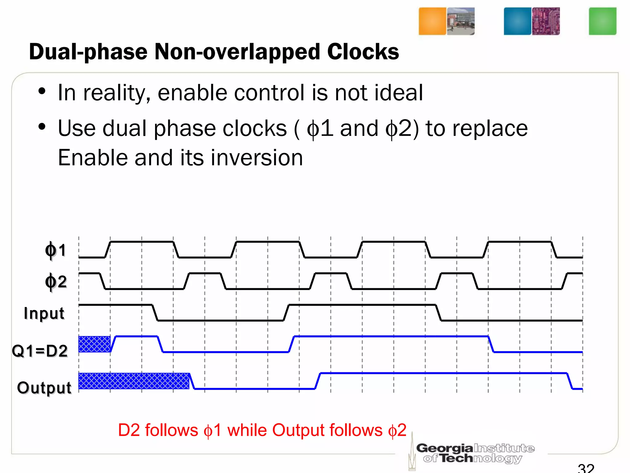
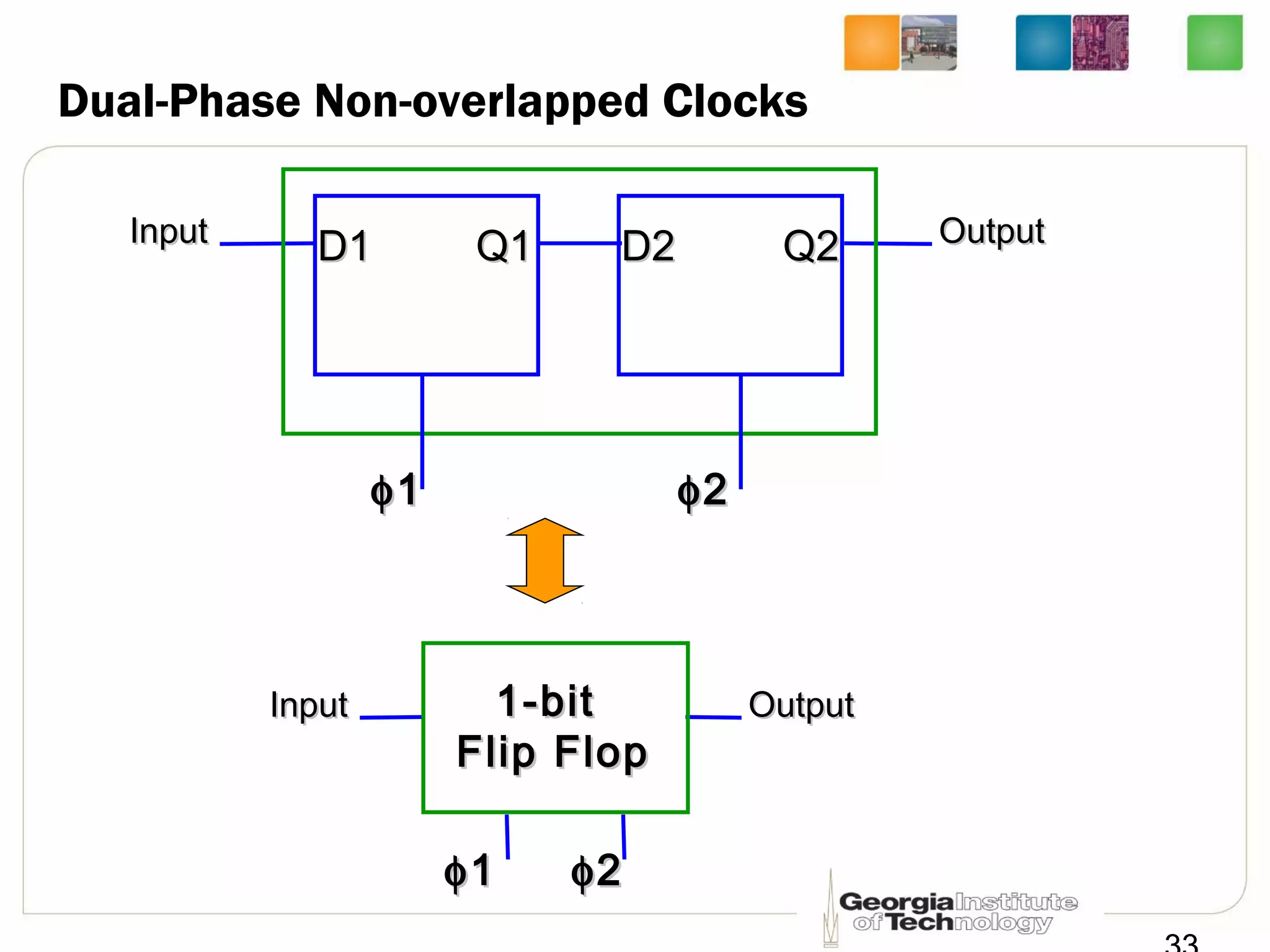
ECE2030
Introduction to Computer Engineering
Lecture 14: Sequential Logic Circuits
Prof. Hsien-Hsin Sean LeeProf. Hsien-Hsin Sean Lee
School of Electrical and Computer EngineeringSchool of Electrical and Computer Engineering
Georgia TechGeorgia Tech
Sequential Logic Circuits
• Sequential circuits
– Combinational logic circuits
– State information (stored in memory)
• Output is a function of inputs and present state
• Can be synchronous or asynchronous
Combinational
circuits
inputs outputs
Storage
Element
delaydelay
PresentPresent
StateState
NextNext
StateState
Controller by a periodic
clock or an event trigger
State machine example
A TV channel control
CH 2CH 2 CH 3CH 3
CH 1CH 1
0
0
1 1
1
0
Sequential Logic Circuits
• Synchronous Circuits use clock pulse to synchronize
• For a typical synchronous design, data are latched into
the storage upon clock transition (edge-triggered)
Combinational
circuits
inputs outputs
Storage
Element
PresentPresent
StateState
NextNext
StateState
clock
Closed-Loop Logic for Storing Information
10
A buffer
Tpd Tpd
XX =
SR Latch
SS
RR
QQ
QQNN
SR Latch
S R Q QN
0 0 Q Q
0 1 0 1
1 0 1 0
1 1 0 0
SS
QQ
QQNN
RR
Reset
Set
Undefined
No Change
SR Latch
S R Q QN
0 0 1 1
0 1 1 0
1 0 0 1
1 1 Q Q
RR
QQ
QQNN
SS
Reset
Set
Undefined
No Change
SR Latch w/ Control
C S R Q QN
0 X X Q Q
1 0 0 Q Q
1 0 1 0 1
1 1 0 1 0
1 1 1 1 1
QQ
QQNN
RR
CC
SS
Reset
Set
Undefined
No Change
No Change
Issue of an SR Latch or SR Latch
SS
QQ
QQNN
RR
SS
RR
S R Q QN
0 0 Q Q
0 1 0 1
1 0 1 0
1 1 0 0
QQ
QQNN
Race, and UnstableRace, and Unstable
D Latch
QQ
QQNN
CC
DD
C D Q QN
0 X Q Q
1 0 0 1
1 1 1 0
D Latch  Keeping Data for Read
QQ
QQ
D Latch  Writing Data DD
DD QQ
QQ
10T D Latch w/ Transmission Gates
DD
EnEn
EnEn
EnEn
QQ
QQ
10T D Latch w/ Transmission Gates
DD
En=1En=1
EnEn
QQ
QQ
DD
Writing Data
DD
DDEnEn
10T D Latch w/ Transmission Gates
D_newD_new
En=0En=0
EnEn
QQ
QQ
Writing Data
DD
DD
DD
EnEn
D Latch Symbol
DD
EnEn
QQ
QQ
En D Q Q
0 X NC NC
1 0 0 1
1 1 1 0
NC: No Change
Latch is Transparent
• D Latch is called “transparent” or “level sensitive”
• Output follows input instantaneously
EnEn
DD
QQ
QQ
Transparent
Transparency Property
DD
EnEn
QQ
Transparent
Latch
DD
EnEn
QQ
Storage
Cell
00
DD
EnEn
QQ
Storage
Cell
11
Latch acts like a WireLatch acts like a Wire
Problem of Transparency
• A momentary input change tunnels through the latch
and the entire circuitry
• What problem this can cause?
DD
EnEn
QQ
TransparentTransparent
LatchLatch
Other LogicOther Logic
CircuitsCircuits
Problem of Transparency
EnEn
TransparentTransparent
LatchLatch
11
DD QQ DD
EnEn
DD
QQ
OscillatingOscillating ⇒⇒ UnstableUnstable UnstableUnstable
Eliminating Transparency
• Separating the input and output, so they are
independently controlled
• Only open one gate at a time to avoid tunneling
EnEn
TransparentTransparent
LatchLatch
DD QQ
EnEn
TransparentTransparent
LatchLatch
DD QQ
Behavior of Master-Slave Latches
EnEn
DD QQ
EnEn
DD QQ
11 00
Storage
Cell
Storage
Cell (00)
EnEn
DD QQ
EnEn
DD QQ
00 11
Storage
Cell (11)
Storage
Cell
Behavior of Master-Slave Latches
EnEn
D1D1 Q1Q1
EnEn
D2D2 Q2Q2
EnEn
D1D1
(initialized to1)(initialized to1)
D1D1
Q1=D2Q1=D2
Q2Q2
A Toggle Cell, will discuss more later
Behavior of Master-Slave Latches
EnEn
D1D1 Q1Q1
EnEn
D2D2 Q2Q2
EnEn
D1D1
(input)(input)
Q1=D2Q1=D2
Q2Q2
Behavior of Master-Slave Latches
EnEn
D1D1 Q1Q1
EnEn
D2D2 Q2Q2
EnEn
Q1=D2Q1=D2
Q2Q2
D1D1
(input)(input)
Flip-Flop (F/F)
D1D1 Q1Q1 D2D2 Q2Q2
Enable (or clock)Enable (or clock)
InputInput OutputOutput
EnableEnable
(or clock)(or clock)
InputInput OutputOutput1-bit1-bit
Flip FlopFlip Flop
Negative Edge Triggered Flip-Flop
D1D1 Q1Q1 D2D2 Q2Q2
clockclock
InputInput
Q1=D2Q1=D2
OutputOutput
Enable (or clock)Enable (or clock)
InputInput OutputOutput
Positive Edge Triggered Flip-Flop
D1D1 Q1Q1 D2D2 Q2Q2
clockclock
Q1=D2Q1=D2
Enable (or clock)Enable (or clock)
InputInput OutputOutput
InputInput
OutputOutput
Positive Edge Triggered Flip-Flop
D1D1 Q1Q1 D2D2 Q2Q2
clockclock
Q1=D2Q1=D2
Enable (or clock)Enable (or clock)
InputInput OutputOutput
InputInput
OutputOutput
Flip Flops Symbols
D
C
Q
Q
D
C
Q
Q
Positive Edge Triggered
D Flip Flop
Negative Edge Triggered
D Flip Flop
Dual-phase Non-overlapped Clocks
• In reality, enable control is not ideal
• Use dual phase clocks ( φ1 and φ2) to replace
Enable and its inversion
φφ11
Q1=D2Q1=D2
InputInput
OutputOutput
φφ22
D2 follows φ1 while Output follows φ2
Dual-Phase Non-overlapped Clocks
D1D1 Q1Q1 D2D2 Q2Q2InputInput OutputOutput
InputInput OutputOutput1-bit1-bit
Flip FlopFlip Flop
φφ11 φφ22
φφ11 φφ22

Lec14 Intro to Computer Engineering by Hsien-Hsin Sean Lee Georgia Tech -- Sequential Logic

  • 1.
    ECE2030 Introduction to ComputerEngineering Lecture 14: Sequential Logic Circuits Prof. Hsien-Hsin Sean LeeProf. Hsien-Hsin Sean Lee School of Electrical and Computer EngineeringSchool of Electrical and Computer Engineering Georgia TechGeorgia Tech
  • 2.
    Sequential Logic Circuits •Sequential circuits – Combinational logic circuits – State information (stored in memory) • Output is a function of inputs and present state • Can be synchronous or asynchronous Combinational circuits inputs outputs Storage Element delaydelay PresentPresent StateState NextNext StateState Controller by a periodic clock or an event trigger
  • 3.
    State machine example ATV channel control CH 2CH 2 CH 3CH 3 CH 1CH 1 0 0 1 1 1 0
  • 4.
    Sequential Logic Circuits •Synchronous Circuits use clock pulse to synchronize • For a typical synchronous design, data are latched into the storage upon clock transition (edge-triggered) Combinational circuits inputs outputs Storage Element PresentPresent StateState NextNext StateState clock
  • 5.
    Closed-Loop Logic forStoring Information 10 A buffer Tpd Tpd XX =
  • 6.
  • 7.
    SR Latch S RQ QN 0 0 Q Q 0 1 0 1 1 0 1 0 1 1 0 0 SS QQ QQNN RR Reset Set Undefined No Change
  • 8.
    SR Latch S RQ QN 0 0 1 1 0 1 1 0 1 0 0 1 1 1 Q Q RR QQ QQNN SS Reset Set Undefined No Change
  • 9.
    SR Latch w/Control C S R Q QN 0 X X Q Q 1 0 0 Q Q 1 0 1 0 1 1 1 0 1 0 1 1 1 1 1 QQ QQNN RR CC SS Reset Set Undefined No Change No Change
  • 10.
    Issue of anSR Latch or SR Latch SS QQ QQNN RR SS RR S R Q QN 0 0 Q Q 0 1 0 1 1 0 1 0 1 1 0 0 QQ QQNN Race, and UnstableRace, and Unstable
  • 11.
    D Latch QQ QQNN CC DD C DQ QN 0 X Q Q 1 0 0 1 1 1 1 0
  • 12.
    D Latch Keeping Data for Read QQ QQ
  • 13.
    D Latch Writing Data DD DD QQ QQ
  • 14.
    10T D Latchw/ Transmission Gates DD EnEn EnEn EnEn QQ QQ
  • 15.
    10T D Latchw/ Transmission Gates DD En=1En=1 EnEn QQ QQ DD Writing Data DD DDEnEn
  • 16.
    10T D Latchw/ Transmission Gates D_newD_new En=0En=0 EnEn QQ QQ Writing Data DD DD DD EnEn
  • 17.
    D Latch Symbol DD EnEn QQ QQ EnD Q Q 0 X NC NC 1 0 0 1 1 1 1 0 NC: No Change
  • 18.
    Latch is Transparent •D Latch is called “transparent” or “level sensitive” • Output follows input instantaneously EnEn DD QQ QQ Transparent
  • 19.
  • 20.
    Problem of Transparency •A momentary input change tunnels through the latch and the entire circuitry • What problem this can cause? DD EnEn QQ TransparentTransparent LatchLatch Other LogicOther Logic CircuitsCircuits
  • 21.
    Problem of Transparency EnEn TransparentTransparent LatchLatch 11 DDQQ DD EnEn DD QQ OscillatingOscillating ⇒⇒ UnstableUnstable UnstableUnstable
  • 22.
    Eliminating Transparency • Separatingthe input and output, so they are independently controlled • Only open one gate at a time to avoid tunneling EnEn TransparentTransparent LatchLatch DD QQ EnEn TransparentTransparent LatchLatch DD QQ
  • 23.
    Behavior of Master-SlaveLatches EnEn DD QQ EnEn DD QQ 11 00 Storage Cell Storage Cell (00) EnEn DD QQ EnEn DD QQ 00 11 Storage Cell (11) Storage Cell
  • 24.
    Behavior of Master-SlaveLatches EnEn D1D1 Q1Q1 EnEn D2D2 Q2Q2 EnEn D1D1 (initialized to1)(initialized to1) D1D1 Q1=D2Q1=D2 Q2Q2 A Toggle Cell, will discuss more later
  • 25.
    Behavior of Master-SlaveLatches EnEn D1D1 Q1Q1 EnEn D2D2 Q2Q2 EnEn D1D1 (input)(input) Q1=D2Q1=D2 Q2Q2
  • 26.
    Behavior of Master-SlaveLatches EnEn D1D1 Q1Q1 EnEn D2D2 Q2Q2 EnEn Q1=D2Q1=D2 Q2Q2 D1D1 (input)(input)
  • 27.
    Flip-Flop (F/F) D1D1 Q1Q1D2D2 Q2Q2 Enable (or clock)Enable (or clock) InputInput OutputOutput EnableEnable (or clock)(or clock) InputInput OutputOutput1-bit1-bit Flip FlopFlip Flop
  • 28.
    Negative Edge TriggeredFlip-Flop D1D1 Q1Q1 D2D2 Q2Q2 clockclock InputInput Q1=D2Q1=D2 OutputOutput Enable (or clock)Enable (or clock) InputInput OutputOutput
  • 29.
    Positive Edge TriggeredFlip-Flop D1D1 Q1Q1 D2D2 Q2Q2 clockclock Q1=D2Q1=D2 Enable (or clock)Enable (or clock) InputInput OutputOutput InputInput OutputOutput
  • 30.
    Positive Edge TriggeredFlip-Flop D1D1 Q1Q1 D2D2 Q2Q2 clockclock Q1=D2Q1=D2 Enable (or clock)Enable (or clock) InputInput OutputOutput InputInput OutputOutput
  • 31.
    Flip Flops Symbols D C Q Q D C Q Q PositiveEdge Triggered D Flip Flop Negative Edge Triggered D Flip Flop
  • 32.
    Dual-phase Non-overlapped Clocks •In reality, enable control is not ideal • Use dual phase clocks ( φ1 and φ2) to replace Enable and its inversion φφ11 Q1=D2Q1=D2 InputInput OutputOutput φφ22 D2 follows φ1 while Output follows φ2
  • 33.
    Dual-Phase Non-overlapped Clocks D1D1Q1Q1 D2D2 Q2Q2InputInput OutputOutput InputInput OutputOutput1-bit1-bit Flip FlopFlip Flop φφ11 φφ22 φφ11 φφ22