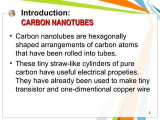
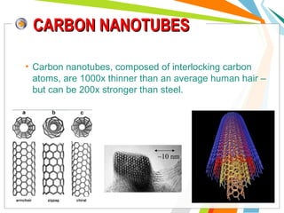
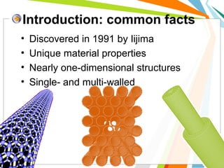
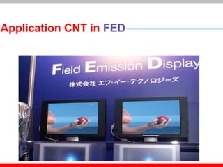
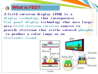
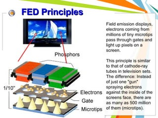
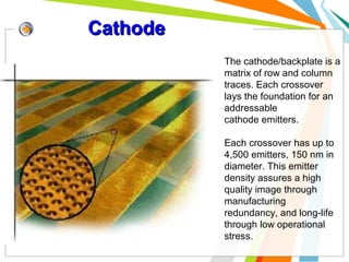
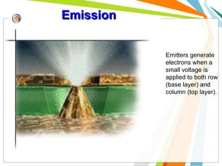
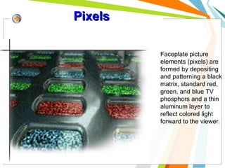
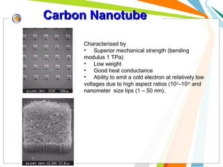
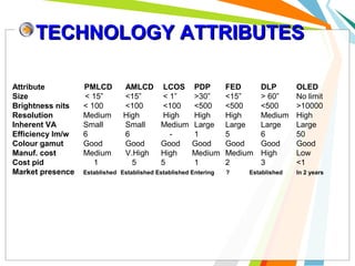
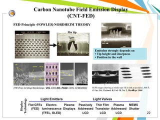
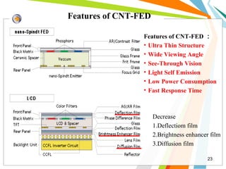
Carbon NanoTube

Applications in FED- Device

Hersh Jalil
MSc. student

L/O/G/O

www.themegallery.com
1
Content
I

What is carbon nanotube (CNT)?

II

Application to field emission display

2
Introduction:
CARBON NANOTUBES
• Carbon nanotubes are hexagonally
shaped arrangements of carbon atoms
that have been rolled into tubes.
• These tiny straw-like cylinders of pure
carbon have useful electrical propeties.
They have already been used to make tiny
transistor and one-dimentional copper wire

3
CARBON NANOTUBES
• Carbon nanotubes, composed of interlocking carbon
atoms, are 1000x thinner than an average human hair –
but can be 200x stronger than steel.

~10 nm
Introduction: common facts
•
•
•
•

Discovered in 1991 by Iijima
Unique material properties
Nearly one-dimensional structures
Single- and multi-walled
Application CNT in FED
What is FED?
A  f i el d em s s i on di s pl ay  ( FED i s a 
i
)
di s pl ay t ec hnol ogy  t hat i nc orporat es  
f l at panel di s pl ay  t ec hnol ogy t hat us es l argearea  f i el d el ec t ron em s s i on  s ourc es t o
i
provi de el ec t rons t hat s t ri ke c ol ored  phos phor
  t o produc e a c ol or i m
age as an 
el ec t roni c vi s ual di s pl ay.  

7
FED Principles
Field emission displays,
electrons coming from
millions of tiny microtips
pass through gates and
light up pixels on a
screen.
This principle is similar
to that of cathode-ray
tubes in television sets.
The difference: Instead
of just one "gun"
spraying electrons
against the inside of the
screens face, there are
as many as 500 million
of them (microtips).
Cathode
The cathode/backplate is a
matrix of row and column
traces. Each crossover
lays the foundation for an
addressable
cathode emitters.
Each crossover has up to
4,500 emitters, 150 nm in
diameter. This emitter
density assures a high
quality image through
manufacturing
redundancy, and long-life
through low operational
stress.
Emission
Emitters generate
electrons when a
small voltage is
applied to both row
(base layer) and
column (top layer).
Pixels
Faceplate picture
elements (pixels) are
formed by depositing
and patterning a black
matrix, standard red,
green, and blue TV
phosphors and a thin
aluminum layer to
reflect colored light
forward to the viewer.
Metal Tips
Theory of CNT-FED
Field Emission Display
Carbon Nanotube
Characterised by
• Superior mechanical strength (bending
modulus 1 TPa)
• Low weight
• Good heat conductance
• Ability to emit a cold electron at relatively low
voltages due to high aspect ratios (102–104) and
nanometer size tips (1 – 50 nm).
ATTRIBUTES
HIGH RESOLUTION
HIGH BRIGHTNESS
LARGE VIEWING ANGLE
HIGH WRITING SPEEDS
LARGE COLOUR GAMUT
HIGH CONTRAST
LESS WEIGHT AND SIZE
LOW POWER CONSUMPTION
LOW COST
The development of Display

FED

PDP

LCD

CRT
Cathode Ray Tube

Liquid Crystal
Display

Field Emission
Display

Plasma Display
Panel

The LCD is the major display technology, and
focused in Japan, Korea and Taiwan.
Then, the others nations want to catch this
market, the FED is more popular in next five
17
years.
FED advantages
Inherently high luminous efficiency
• high contrast levels
• very fast response times
• Lower Power Consumption
• about half that of an LCD system
– Cold Cathode Emission
– Distance between cathode and screen
~0.2–5mm

Technology

CRT (at
30KV)

Luminous
Efficiency
(Lm/W)
3

PDP

0.8

LCD

3

OLED / PLED

5

FED at 8 KV
• Capital investment for
manufacturing VLS TV with
printable CNT FEDs - 1/10th of LCD
• Cost advantage over LCD could be
40%

7
FED Technology Roadblocks
• Spindt type FED
– Yield problems – Tip wear off, high vacuum
– High cost of submicron technology for Spindt
type emitters
– High Voltage Breakdown due to electron
bombardment and spacer charging
– Phosphor decay in case anode is at low
voltage to counter the above problem
– Backscatter from anodes at high anode
voltages leading to cross talk
TECHNOLOGY ATTRIBUTES
Attribute
Size
Brightness nits
Resolution
Inherent VA
Efficiency lm/w
Colour gamut
Manuf. cost
Cost pid
Market presence

PMLCD
< 15”
< 100
Medium
Small
6
Good
Medium
1

AMLCD
<15”
<100
High
Small
6
Good
V.High
5

LCOS
< 1”
<100
High
Medium
Good
High
5

PDP
>30”
<500
High
Large
1
Good
Medium
1

Established Established Established Entering

FED
<15”
<500
High
Large
5
Good
Medium
2
?

DLP
> 60”
<500
Medium
Large
6
Good
High
3

Established

OLED
No limit
>10000
High
Large
50
Good
Low
<1
In 2 years
The SEM image of CNT-FED

Zoom in

21
Carbon Nanotube Field Emission Display
(CNT-FED)
FED Principle -FOWLER-NORDHEIM THEORY
Mo tip
1μm

Emission strongly depends on
• Tip height and sharpness
• Position in the well

Display
Technology

ITRI Proc Int Disp Workshops VOL.10th;NO.;PAGE.1195-1198(2003)

SEM images showing a triode type FEA with a tip radius ,400 Å
J. Vac. Sci. Technol. B, Vol. 18, No. 2, MarÕApr 2000

22
Features of CNT-FED
Features of CNT-FED :
• Ultra Thin Structure
• Wide Viewing Angle
• See-Through Vision
• Light Self Emission
• Low Power Consumption
• Fast Response Time

Decrease
1.Deflectiom film
2.Brightness enhancer film
3.Diffusion film
23
Thanks for you

!!

Cnt application in fed

  • 1.
    Carbon NanoTube Applications inFED- Device Hersh Jalil MSc. student L/O/G/O www.themegallery.com 1
  • 2.
    Content I What is carbonnanotube (CNT)? II Application to field emission display 2
  • 3.
    Introduction: CARBON NANOTUBES • Carbonnanotubes are hexagonally shaped arrangements of carbon atoms that have been rolled into tubes. • These tiny straw-like cylinders of pure carbon have useful electrical propeties. They have already been used to make tiny transistor and one-dimentional copper wire 3
  • 4.
    CARBON NANOTUBES • Carbonnanotubes, composed of interlocking carbon atoms, are 1000x thinner than an average human hair – but can be 200x stronger than steel. ~10 nm
  • 5.
    Introduction: common facts • • • • Discoveredin 1991 by Iijima Unique material properties Nearly one-dimensional structures Single- and multi-walled
  • 6.
  • 7.
    What is FED? A f i el d em s s i on di s pl ay  ( FED i s a  i ) di s pl ay t ec hnol ogy  t hat i nc orporat es   f l at panel di s pl ay  t ec hnol ogy t hat us es l argearea  f i el d el ec t ron em s s i on  s ourc es t o i provi de el ec t rons t hat s t ri ke c ol ored  phos phor   t o produc e a c ol or i m age as an  el ec t roni c vi s ual di s pl ay.   7
  • 8.
    FED Principles Field emissiondisplays, electrons coming from millions of tiny microtips pass through gates and light up pixels on a screen. This principle is similar to that of cathode-ray tubes in television sets. The difference: Instead of just one "gun" spraying electrons against the inside of the screens face, there are as many as 500 million of them (microtips).
  • 9.
    Cathode The cathode/backplate isa matrix of row and column traces. Each crossover lays the foundation for an addressable cathode emitters. Each crossover has up to 4,500 emitters, 150 nm in diameter. This emitter density assures a high quality image through manufacturing redundancy, and long-life through low operational stress.
  • 10.
    Emission Emitters generate electrons whena small voltage is applied to both row (base layer) and column (top layer).
  • 11.
    Pixels Faceplate picture elements (pixels)are formed by depositing and patterning a black matrix, standard red, green, and blue TV phosphors and a thin aluminum layer to reflect colored light forward to the viewer.
  • 12.
  • 13.
  • 14.
  • 15.
    Carbon Nanotube Characterised by •Superior mechanical strength (bending modulus 1 TPa) • Low weight • Good heat conductance • Ability to emit a cold electron at relatively low voltages due to high aspect ratios (102–104) and nanometer size tips (1 – 50 nm).
  • 16.
    ATTRIBUTES HIGH RESOLUTION HIGH BRIGHTNESS LARGEVIEWING ANGLE HIGH WRITING SPEEDS LARGE COLOUR GAMUT HIGH CONTRAST LESS WEIGHT AND SIZE LOW POWER CONSUMPTION LOW COST
  • 17.
    The development ofDisplay FED PDP LCD CRT Cathode Ray Tube Liquid Crystal Display Field Emission Display Plasma Display Panel The LCD is the major display technology, and focused in Japan, Korea and Taiwan. Then, the others nations want to catch this market, the FED is more popular in next five 17 years.
  • 18.
    FED advantages Inherently highluminous efficiency • high contrast levels • very fast response times • Lower Power Consumption • about half that of an LCD system – Cold Cathode Emission – Distance between cathode and screen ~0.2–5mm Technology CRT (at 30KV) Luminous Efficiency (Lm/W) 3 PDP 0.8 LCD 3 OLED / PLED 5 FED at 8 KV • Capital investment for manufacturing VLS TV with printable CNT FEDs - 1/10th of LCD • Cost advantage over LCD could be 40% 7
  • 19.
    FED Technology Roadblocks •Spindt type FED – Yield problems – Tip wear off, high vacuum – High cost of submicron technology for Spindt type emitters – High Voltage Breakdown due to electron bombardment and spacer charging – Phosphor decay in case anode is at low voltage to counter the above problem – Backscatter from anodes at high anode voltages leading to cross talk
  • 20.
    TECHNOLOGY ATTRIBUTES Attribute Size Brightness nits Resolution InherentVA Efficiency lm/w Colour gamut Manuf. cost Cost pid Market presence PMLCD < 15” < 100 Medium Small 6 Good Medium 1 AMLCD <15” <100 High Small 6 Good V.High 5 LCOS < 1” <100 High Medium Good High 5 PDP >30” <500 High Large 1 Good Medium 1 Established Established Established Entering FED <15” <500 High Large 5 Good Medium 2 ? DLP > 60” <500 Medium Large 6 Good High 3 Established OLED No limit >10000 High Large 50 Good Low <1 In 2 years
  • 21.
    The SEM imageof CNT-FED Zoom in 21
  • 22.
    Carbon Nanotube FieldEmission Display (CNT-FED) FED Principle -FOWLER-NORDHEIM THEORY Mo tip 1μm Emission strongly depends on • Tip height and sharpness • Position in the well Display Technology ITRI Proc Int Disp Workshops VOL.10th;NO.;PAGE.1195-1198(2003) SEM images showing a triode type FEA with a tip radius ,400 Å J. Vac. Sci. Technol. B, Vol. 18, No. 2, MarÕApr 2000 22
  • 23.
    Features of CNT-FED Featuresof CNT-FED : • Ultra Thin Structure • Wide Viewing Angle • See-Through Vision • Light Self Emission • Low Power Consumption • Fast Response Time Decrease 1.Deflectiom film 2.Brightness enhancer film 3.Diffusion film 23
  • 24.

Editor's Notes