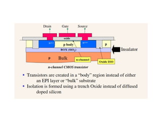
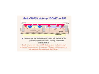
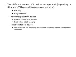
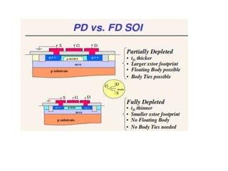
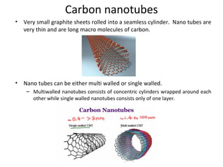
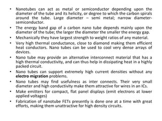
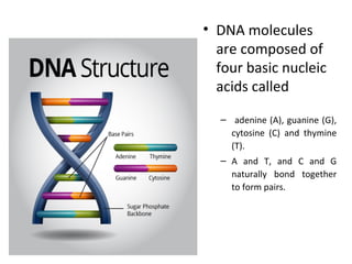
SlideShare a Scribd company logo
Beyond CMOS
Mr.Narayana Swamy.R
Assoc.Prof,Dept of ECE
T.John Institute of Technology, Bangalore
Evolutionary advances beyond CMOS
• Evolutionary approaches-Silicon on Insulator, Dual gate FETs and SiGe
structures.
• SOI
– Consists of thin SiFET structure grown on a buried SiO2 layer which is in turn grown on a
Si substrate.
– Complete electrical isolation,
– Eliminating latch up between adjacent devices (electrical behavior (electrical
interaction can occur between neighboring tubs and/or the substrate) of one
device affects that of a neighboring device),
– Rad-hard or radiation hardness-Highly immune to radiation induced failure,
such as soft errors (change in logic state of a device due to the accumulation
of charge resulting from carrier generation following the transit of a high
energy particle or ionizing radiation through the device),
– Immune to short channel effects than standard CMOS,
• Two different manner SOI devices are operated (depending on
thickness of Si layer and its doping concentration)
• Partially
• Fully depleted
– Partially depleted SOI devices
• Made with thicker Si active layers
• Disadvantage is body charging
– Fully Depleted SOI devices
• Thin active layer and the doping concentration sufficiently low that it is depleted of
free carriers.
• Dual gate FET
– Short channel effects are reduced
– Reduce the drain-induced barrier lowering and minimize threshold sensitivity to the
channel
– Relative Scaling advantage of about a factor of 2 over conventional CMOS devices
– Disadvantage presence of two si-sio2 interfaces from two gates increases the surface
roughness scattering. As a result the carrier mobility is reduced thus lowering the
frequency of operation of the device.
– Two different types of dual gate MOSFET structures -Symmetric and asymmetric gated
devices
• Surface channels turn on at same gate voltages -Same work function
• Surface channels turn on at different gate voltages - different work function
– Three different ways in which dual gate MOSFET can be made
• With top and bottom gates formed parallel to the plane of the substrate. In this configuration the source and
drain regions straddle the two gates and the current flow in the channel runs parallel to the substrate.
• Vertical dual gate FETs the gates are perpendicular to the substrate and the current runs parallel to the
substrate- FinFET
• Si and Si-Ge together to form heterostructure.The enhanced electron mobility within the strained Si acts to
increase the speed of the SiGe MOSFET. Therefore, strained Si-SiGe MOSFETs have an intrinsically higher
transconductance and thus higher frequency of operation than conventional MOSFETs.
WHAT IS SHORT CHANNEL
• Channel length ~= depletion width of source and drain
• Short channel MOS has good processing speed, requires low operating potential and
increases transistor density on the chip.
• Although the performance degrades with decrease in channel length.
• It faces some serious issues like DIBL, surface scattering, velocity saturation, impact
ionisation, hot electron effect
DRAIN INDUCED BARRIER
LOWERING(DIBL)
SURFACE SCATTERING
• In long channel Ex>>Ey, but in short channel Ex is not negligible.
• Ex and Ey field makes electron to travel in zig-zag path, reducing their mobility.
• As the channel length becomes shorter electric field Ey increases causing surface
mobility to become field dependent.
Carbon nanotubes
• Very small graphite sheets rolled into a seamless cylinder. Nano tubes are
very thin and are long macro molecules of carbon.
• Nano tubes can be either multi walled or single walled.
– Multiwalled nanotubes consists of concentric cylinders wrapped around each
other while single walled nanotubes consists only of one layer.
• Nanotubes can act as metal or semiconductor depending upon the
diameter of the tube and its helicity, or degree to which the carbon spirals
around the tube. Large diameter – semi metal; narrow diameter-
semiconductor.
• The energy band gap of a carbon nano tube depends mainly upon the
diameter of the tube; the larger the diameter the smaller the energy gap.
• Mechanically they have largest strength to weight ratios of any material.
• Very high thermal conductance, close to diamond making them efficient
heat conductors. Nano tubes can be used to cool very dense arrays of
devices.
• Nano tube may provide an alternative interconnect material that has a
high thermal conductivity, and can thus help in dissipating heat in a highly
packed circuit.
• Nano tubes can support extremely high current densities without any
electro migration problems.
• Nano tubes may find usefulness as inter connects. Their very small
diameter and high conductivity make them attractive for wires in an ICs.
• Make emitters for compact, flat panel displays (emit electrons at lower
applied voltages)
• Fabrication of nanotube FETs presently is done one at a time with great
efforts, making them unattractive for high density circuits.
• Nano tube FET device
In this structure a single SWCNT was used to bridge two noble metal electrodes
prefabricated by lithography on an oxidized silicon wafer. Here the SWCNT plays the
role of channel and the metal electrodes act as source and drain. The heavily doped
silicon wafer itself behaves as the back gate. These CNTFETs behaved as p-type
FETs with an I (on)/I(off) ratio~105. This suffers from some of the limitations like high
parasitic contact resistance (=1Mohm), low drive currents (a few Nanoamperes), and
low transconductance. To reduce these limitations the next generation CNTFET
developed which is known as top gate CNTFET.
Conventional vs tactile computing, molecular
and biological computing
Conventional Computers
• Conventional computers are machines that follow a well
described set of instructions to process data.
• Basically, a set of instructions is read into the machine and it
works sequentially in an ordered way to execute a task.
• often referred to as Von Neumann computers or classical
machines.
• major components are
– memory,
– processing, and
– bandwidth.
Continued…..
• Can be thought of as structurally programmable machines.
This means that the program controls the behavior of the
machine.
• A compiler translates the input code into machine language
that is expressed in terms of the states of simple switching
devices and their connections.
• The machine computes symbolically and the result depends
to some extent upon the human input.
 Well suited to number crunching, communication, and data
manipulation.
19
Problems
• pattern recognition
– Specifically, it is very difficult to program a classical computer to recognize
a complicated molecule or distinguish between different microorganisms.
• In the chemical and biological world pattern recognition is highly
efficient and readily accomplished.
– For example, the immune system in the human body. This behavior is an
example of a different type of computing, which we will refer to as tactile
computing.
20
Tactile Computing
• These machines are not structurally programmable.
• In Bio molecular computing, pattern processing is physical and
dynamic as opposed to the symbolic and passive processing in a
conventional machine.
• Programming depends upon evolution by variation and
selection. Such a molecular computer is called a tactile
processor.
• A tactile processor can be thought of as a computer driven by
enzymes; the inputs are converted into molecular shapes that
the enzymes can recognize.
• Enzyme thus performs sophisticated pattern recognition since it
scans the molecular objects within its environment, interacting
with only those molecules that have a complementary shape
• Recognition is thus a tactile procedure.21
Examples
1) An example of tactile computer-
– A variety of bacteria bred to dissolve oil spills.
– the bacteria would be “programmed” by altering its DNA.
– the unique and powerful information processing capabilities of life,
pattern and object recognition, self-organization and learning, and
effective use of parallelism are harnessed.
2) sensing bioagents or toxins.
– Molecules can be used to perform complicated pattern recognition of
dangerous toxins released into the air or water.
– Even Very dilute amounts can be identified readily.
– Can be used to fight terrorist bioattacks, or chemical warfare.
• The “program” is in the molecule itself; the computation occurs
by the recognition of one molecule by an enzyme and their
subsequent chemical reaction.
• Next we will examine tactile computing using biological systems,
DNA, and molecules.
22
Biomolecular Computing
• Biological systems are a special case of molecular computing(broader
context).
• Major qualities of molecules that make their potential usage in future
applications attractive are that they offer simplified fabrication, low cost
and relatively unlimited availability, and devices made from molecules are
very much smaller and compact than existing CMOS structures.
• For example
– A CMOS OR gate requires any where from 4-6 orders of magnitude more
surface area than a comparable molecular logic gate.
– Molecular electronic offers extremely compact computing capability,i.e
Microprocessor on a pinhead. Coupled with their expected lower power
consumption and relatively inexpensive to fabricate and mass produce.
23
key advantages of molecular materials
• Size: on average they are about 4 nm. These device dimensions are about
two orders of magnitude smaller than that which can be obtained using
SiCMOStechnology.
• Three-dimensional structures: In contrast, in Si based technology, much
fabrication effort and cost is required to produce three-dimensional
geometries.
• High packing density: the combined features of small size and three-
dimensionality make very high packing densities possible. It is estimated
that the packing density can be increased by 6–9 orders of magnitude
over CMOS.
• Bistability and nonlinearity: bistability and nonlinearity can be utilized to
perform switching functions. Both of these properties are commonly
available in molecules.
• Anisotropy: the electronic and optical properties of a molecule are
inherent in the molecular structure instead of being fabricated by the
processing technologies as in CMOS.
24
Continued…..
• Upward construction: organic synthesis enables growth of
microstructures from the small upward. In standard CMOS, device and
circuit functionality is sculpted from a relatively large piece of material.
• Self-organization: self-organization, self-synthesis, and redundancy
factors well known in organic and biological molecules that could
potentially be applied to molecular electronic devices.
• Low power dissipation: Estimates are that the total power requirements
for molecular switches will be about five orders of magnitude lower than
for CMOS switches.
• Molecular engineering: it is possible that molecules can be tailored or
engineered(can be selectively grown and made to inherently possess
desired qualities to perform a task.) to perform specific tasks or have
specific properties.
The above features of molecules also apply to biomolecules.
25
Bio molecules
• Bio molecules provide parallel environment for computation, they occur
abundantly in nature and their implementation due to self organization and
upward construction is relatively simple compared with the difficult and costly
fabrication of CMOS circuitry.
• As mentioned size is a key advantage of molecules.
– The entire genetic code for humans is contained in the nucleus of most cells.
– The DNA Code consists of over three billion nucleotide pairs and fits into a few double helices about
3.4nm in width and measuring micrometers in length.
26
DNA-an overview
• The entire genetic code for humans is contained in the
nucleus of most cells.
• The DNA code consists of over three billion nucleotide pairs
and fits into a few double helices about 3.4 nm in width and
measuring micrometers in length.
27
• Researchers are developing what are called applets for biological
systems.
• These applets enable the system to respond to an external event,
“program” a cell to produce a desired chemical or enzyme, or
enable a cell to identify a reagent.
• Some potential applications of biological applets:
– In gene therapy for treating diseases such as hemophilia,
anemia, etc.
– in the treatment of diabetes( A genetic applet can be used
that senses the glucose level in the blood and another applet
can then direct the production and release of insulin if
needed.).
28
• DNA molecules
are composed of
four basic nucleic
acids called
– adenine (A), guanine (G),
cytosine (C) and thymine
(T).
– A and T, and C and G
naturally bond together
to form pairs.
29
Computation with DNA
• To compute with DNA there are three basic steps.
– encoding that maps the problem onto DNA strands,
– basic processing using a chemical process called
hybridization that connects two complementary DNA
strands into a double strand,
– and outputting the results.
 Programming DNA involves the usage of DNA tiles.
• These tiles consist of multiple strands of DNA knotted
together.
• The ends of each tile are created such that the tile will
recognize and attach to other pre-designed tiles to make self-
assembled structures.
• These tiles can be used to add or multiply numbers30
Drawbacks
• These are basically related to the difficulty encountered in
regulating or controlling the basic chemistry.
– Reliability means the degree of confidence in correctly
solving a problem.
– Efficiency is related to the effective manipulation of the
molecules used to perform the computation.
– Scalability is the successful reproduction of the desired
event many times.
31
Moletronics-molecular diodes and diode-diode logic
• Both conducting and insulating molecules are needed to form
devices.
• Two most conducting molecular species are polyphenylenes
and carbon nanotubes.
• Polyphenylenes are chain like molecules formed by linking a
basic molecular unit, C6H4 , phenylene, which is a derivative of
the benzene ring but with two free binding sites
• Molecules can also be used to build devices that mimic CMOS
functionality.
• Molecular diodes and other quantum based devices have
been designed.
• The primary components of these molecular structures are
conducting groups called polyphenylenes and insulating
groups called aliphatic molecules.
• By arranging these molecules in various orders similar device
action to that found in semiconductors can be attained.
• These structures can be combined to make various logic gates
such as NOR and NAND gates.
33
Defect tolerant computing
• Wherein the operation of a computer can be maintained even if part of its
hardware is defective.
• Yield of the chips, defined as the percentage of perfectly operating chips vs the
total number made on the die, decreases with increasing chip complexity.
• The ability to configure a chip to operate around defects and imperfections would
greatly improve the manufacturing yield and consequently the cost of the chips.
• Existing computing hardware paradigm is that the chip must function in all
applications perfectly ( perfect performance).
• The perfectly operating chip paradigm is not the only possibility for computing
hardware. It is conceivable that flawed chips can still be used provided that the
defective components in the chip are known in advance and are thereby avoided
during chip’s operation. Such an approach is called defect tolerant computing.
• Teramac 10^12 operations per second-many defective chips could be connected12 operations per second-many defective chips could be connected
to produce a powerful yet very inexpensive parallel computer.to produce a powerful yet very inexpensive parallel computer.
• Family tree like branching architecture and fat-tree architecture.Family tree like branching architecture and fat-tree architecture.
• Teramac utilizes Fat-tree architecture.Teramac utilizes Fat-tree architecture.

More Related Content

What's hot

Energy band diagram
Energy band diagramEnergy band diagram
Energy band diagram
Bkannan2
 
Nmi Presentation Sept 2007
Nmi Presentation Sept 2007Nmi Presentation Sept 2007
Nmi Presentation Sept 2007
AdrianOShaughnessy
 
Semiconductor overview
Semiconductor overviewSemiconductor overview
Semiconductor overview
Nabil Chouba
 
Cmos process flow
Cmos process flowCmos process flow
Cmos process flow
Bhargav Veepuri
 
Metallization
Metallization Metallization
Metallization
GKGanesh2
 
Optical network architecture
Optical network architectureOptical network architecture
Optical network architecture
Siddharth Singh
 
MOSFET, SOI-FET and FIN-FET-ABU SYED KUET
MOSFET, SOI-FET and FIN-FET-ABU SYED KUETMOSFET, SOI-FET and FIN-FET-ABU SYED KUET
MOSFET, SOI-FET and FIN-FET-ABU SYED KUET
A. S. M. Jannatul Islam
 
Public Presentation, ASML DB Conference Singapore
Public Presentation, ASML DB Conference SingaporePublic Presentation, ASML DB Conference Singapore
Public Presentation, ASML DB Conference Singapore
JVervoort
 
CMOS LOGIC STRUCTURES
CMOS LOGIC STRUCTURESCMOS LOGIC STRUCTURES
CMOS LOGIC STRUCTURES
VaishaliVaishali14
 
VLSI Design(Fabrication)
VLSI Design(Fabrication)VLSI Design(Fabrication)
VLSI Design(Fabrication)
Trijit Mallick
 
Epitaxial growth - Fabrication
Epitaxial growth - FabricationEpitaxial growth - Fabrication
Epitaxial growth - Fabrication
Md. Rayid Hasan Mojumder
 
Device isolation Techniques
Device isolation TechniquesDevice isolation Techniques
Device isolation Techniques
Sudhanshu Janwadkar
 
1. Massive Machine-Type Communication.pptx
1. Massive Machine-Type Communication.pptx1. Massive Machine-Type Communication.pptx
1. Massive Machine-Type Communication.pptx
Sri Manakula Vinayagar Engineering College
 
Fully depleted silicon insulator
Fully depleted silicon insulatorFully depleted silicon insulator
Fully depleted silicon insulator
sandeep sandy
 
MOS as Diode, Switch and Active Resistor
MOS as Diode, Switch and Active ResistorMOS as Diode, Switch and Active Resistor
MOS as Diode, Switch and Active Resistor
Sudhanshu Janwadkar
 
CMOS Logic
CMOS LogicCMOS Logic
Junctionless transistors
Junctionless transistorsJunctionless transistors
Junctionless transistors
Pratishtha Agnihotri
 
MRAM & Its Applications
MRAM & Its ApplicationsMRAM & Its Applications
MRAM & Its Applications
Tariq Tauheed
 
microwave integrated circuit
microwave integrated circuitmicrowave integrated circuit
microwave integrated circuit
Radha Mahalle
 
faults in digital systems
faults in digital systemsfaults in digital systems
faults in digital systems
dennis gookyi
 

What's hot (20)

Energy band diagram
Energy band diagramEnergy band diagram
Energy band diagram
 
Nmi Presentation Sept 2007
Nmi Presentation Sept 2007Nmi Presentation Sept 2007
Nmi Presentation Sept 2007
 
Semiconductor overview
Semiconductor overviewSemiconductor overview
Semiconductor overview
 
Cmos process flow
Cmos process flowCmos process flow
Cmos process flow
 
Metallization
Metallization Metallization
Metallization
 
Optical network architecture
Optical network architectureOptical network architecture
Optical network architecture
 
MOSFET, SOI-FET and FIN-FET-ABU SYED KUET
MOSFET, SOI-FET and FIN-FET-ABU SYED KUETMOSFET, SOI-FET and FIN-FET-ABU SYED KUET
MOSFET, SOI-FET and FIN-FET-ABU SYED KUET
 
Public Presentation, ASML DB Conference Singapore
Public Presentation, ASML DB Conference SingaporePublic Presentation, ASML DB Conference Singapore
Public Presentation, ASML DB Conference Singapore
 
CMOS LOGIC STRUCTURES
CMOS LOGIC STRUCTURESCMOS LOGIC STRUCTURES
CMOS LOGIC STRUCTURES
 
VLSI Design(Fabrication)
VLSI Design(Fabrication)VLSI Design(Fabrication)
VLSI Design(Fabrication)
 
Epitaxial growth - Fabrication
Epitaxial growth - FabricationEpitaxial growth - Fabrication
Epitaxial growth - Fabrication
 
Device isolation Techniques
Device isolation TechniquesDevice isolation Techniques
Device isolation Techniques
 
1. Massive Machine-Type Communication.pptx
1. Massive Machine-Type Communication.pptx1. Massive Machine-Type Communication.pptx
1. Massive Machine-Type Communication.pptx
 
Fully depleted silicon insulator
Fully depleted silicon insulatorFully depleted silicon insulator
Fully depleted silicon insulator
 
MOS as Diode, Switch and Active Resistor
MOS as Diode, Switch and Active ResistorMOS as Diode, Switch and Active Resistor
MOS as Diode, Switch and Active Resistor
 
CMOS Logic
CMOS LogicCMOS Logic
CMOS Logic
 
Junctionless transistors
Junctionless transistorsJunctionless transistors
Junctionless transistors
 
MRAM & Its Applications
MRAM & Its ApplicationsMRAM & Its Applications
MRAM & Its Applications
 
microwave integrated circuit
microwave integrated circuitmicrowave integrated circuit
microwave integrated circuit
 
faults in digital systems
faults in digital systemsfaults in digital systems
faults in digital systems
 

Viewers also liked

Soi cmos device technology
Soi cmos device technologySoi cmos device technology
Soi cmos device technology
Đình Khanh Nguyễn
 
Ultra Thin Body SOI FETs
Ultra Thin Body SOI FETsUltra Thin Body SOI FETs
Ultra Thin Body SOI FETs
sindhu reddy
 
Ultra-thin body SOI MOSFETs: Term Paper_class presentation on Advanced topics...
Ultra-thin body SOI MOSFETs: Term Paper_class presentation on Advanced topics...Ultra-thin body SOI MOSFETs: Term Paper_class presentation on Advanced topics...
Ultra-thin body SOI MOSFETs: Term Paper_class presentation on Advanced topics...
prajon
 
CMOS N P Twin Tub Well Formation
CMOS N P Twin Tub Well FormationCMOS N P Twin Tub Well Formation
CMOS N P Twin Tub Well Formation
azmathmoosa
 
Fabrication of silicon on insulator (soi)
Fabrication of silicon on insulator (soi)Fabrication of silicon on insulator (soi)
Fabrication of silicon on insulator (soi)
Pooja Shukla
 
Twin well process
Twin well processTwin well process
Twin well process
dragonpradeep
 
SOI
SOISOI
twin well cmos fabrication steps using Synopsys TCAD
twin well cmos fabrication steps using Synopsys TCADtwin well cmos fabrication steps using Synopsys TCAD
twin well cmos fabrication steps using Synopsys TCAD
Team-VLSI-ITMU
 
CMOS SOI Technology
CMOS SOI TechnologyCMOS SOI Technology
CMOS SOI Technology
mehdisimoussa
 
CMOS VLSI design
CMOS VLSI designCMOS VLSI design
CMOS VLSI design
Rajan Kumar
 

Viewers also liked (10)

Soi cmos device technology
Soi cmos device technologySoi cmos device technology
Soi cmos device technology
 
Ultra Thin Body SOI FETs
Ultra Thin Body SOI FETsUltra Thin Body SOI FETs
Ultra Thin Body SOI FETs
 
Ultra-thin body SOI MOSFETs: Term Paper_class presentation on Advanced topics...
Ultra-thin body SOI MOSFETs: Term Paper_class presentation on Advanced topics...Ultra-thin body SOI MOSFETs: Term Paper_class presentation on Advanced topics...
Ultra-thin body SOI MOSFETs: Term Paper_class presentation on Advanced topics...
 
CMOS N P Twin Tub Well Formation
CMOS N P Twin Tub Well FormationCMOS N P Twin Tub Well Formation
CMOS N P Twin Tub Well Formation
 
Fabrication of silicon on insulator (soi)
Fabrication of silicon on insulator (soi)Fabrication of silicon on insulator (soi)
Fabrication of silicon on insulator (soi)
 
Twin well process
Twin well processTwin well process
Twin well process
 
SOI
SOISOI
SOI
 
twin well cmos fabrication steps using Synopsys TCAD
twin well cmos fabrication steps using Synopsys TCADtwin well cmos fabrication steps using Synopsys TCAD
twin well cmos fabrication steps using Synopsys TCAD
 
CMOS SOI Technology
CMOS SOI TechnologyCMOS SOI Technology
CMOS SOI Technology
 
CMOS VLSI design
CMOS VLSI designCMOS VLSI design
CMOS VLSI design
 

Similar to Beyond cmos

Nanotechnology
NanotechnologyNanotechnology
Nanotechnology
Techef In
 
Nanoscale Based Digital VLSI Circuits (1) - NEHA PATEL.pptx.pdf
Nanoscale Based Digital VLSI Circuits (1) - NEHA PATEL.pptx.pdfNanoscale Based Digital VLSI Circuits (1) - NEHA PATEL.pptx.pdf
Nanoscale Based Digital VLSI Circuits (1) - NEHA PATEL.pptx.pdf
batpad
 
Viii. molecular electronics and nanoscience
Viii. molecular electronics and nanoscienceViii. molecular electronics and nanoscience
Viii. molecular electronics and nanoscience
AllenHermann
 
Nano devices- resonant tunneling diode, resonant tunneling transistor, SET, F...
Nano devices- resonant tunneling diode, resonant tunneling transistor, SET, F...Nano devices- resonant tunneling diode, resonant tunneling transistor, SET, F...
Nano devices- resonant tunneling diode, resonant tunneling transistor, SET, F...
pondicherry university
 
VLSI-Design.pdf
VLSI-Design.pdfVLSI-Design.pdf
VLSI-Design.pdf
AcademicICECE
 
Epitaxial Growth
Epitaxial GrowthEpitaxial Growth
Rosh ppt
Rosh pptRosh ppt
Rosh ppt
Rosh Mani
 
Nano electronics Technology and its Application
Nano electronics Technology and its ApplicationNano electronics Technology and its Application
Nano electronics Technology and its Application
Seelam Vasavi Sai Viswanada Prabhu Deva Kumar
 
Carbon nanotube based Field Effect Transistor
Carbon nanotube based Field Effect TransistorCarbon nanotube based Field Effect Transistor
Carbon nanotube based Field Effect Transistor
Sushmita Dandeliya
 
Please read the following IEEE Spectrum articles and answer the quest.pdf
Please read the following IEEE Spectrum articles and answer the quest.pdfPlease read the following IEEE Spectrum articles and answer the quest.pdf
Please read the following IEEE Spectrum articles and answer the quest.pdf
fasttrackcomputersol
 
18EC655_Module-1.pptx
18EC655_Module-1.pptx18EC655_Module-1.pptx
18EC655_Module-1.pptx
JazzSameer
 
UNIT-1 VLSID-MREC-ECE-Dr.TM.pptx
UNIT-1 VLSID-MREC-ECE-Dr.TM.pptxUNIT-1 VLSID-MREC-ECE-Dr.TM.pptx
UNIT-1 VLSID-MREC-ECE-Dr.TM.pptx
8885684828
 
Carbon nanotubes ppt
Carbon nanotubes pptCarbon nanotubes ppt
Carbon nanotubes ppt
Amal Ray
 
Ele cproject final
Ele cproject finalEle cproject final
Ele cproject final
CHETHANA JOHANS
 
Moletronics
MoletronicsMoletronics
Moletronics
maddyz03
 
My VLSI.pptx
My VLSI.pptxMy VLSI.pptx
My VLSI.pptx
chiranjeevimuppala2
 
MESOSCOPIC STRUCTURE.pptx
MESOSCOPIC STRUCTURE.pptxMESOSCOPIC STRUCTURE.pptx
MESOSCOPIC STRUCTURE.pptx
AstronautKennedy
 
Nanotechnology.Opport.Dev
Nanotechnology.Opport.DevNanotechnology.Opport.Dev
Nanotechnology.Opport.Dev
lusik
 
PLASMONICS
PLASMONICSPLASMONICS
PLASMONICS
Vijitha J
 
Nanoelectronics
NanoelectronicsNanoelectronics
Nanoelectronics
Viju Jigajinni
 

Similar to Beyond cmos (20)

Nanotechnology
NanotechnologyNanotechnology
Nanotechnology
 
Nanoscale Based Digital VLSI Circuits (1) - NEHA PATEL.pptx.pdf
Nanoscale Based Digital VLSI Circuits (1) - NEHA PATEL.pptx.pdfNanoscale Based Digital VLSI Circuits (1) - NEHA PATEL.pptx.pdf
Nanoscale Based Digital VLSI Circuits (1) - NEHA PATEL.pptx.pdf
 
Viii. molecular electronics and nanoscience
Viii. molecular electronics and nanoscienceViii. molecular electronics and nanoscience
Viii. molecular electronics and nanoscience
 
Nano devices- resonant tunneling diode, resonant tunneling transistor, SET, F...
Nano devices- resonant tunneling diode, resonant tunneling transistor, SET, F...Nano devices- resonant tunneling diode, resonant tunneling transistor, SET, F...
Nano devices- resonant tunneling diode, resonant tunneling transistor, SET, F...
 
VLSI-Design.pdf
VLSI-Design.pdfVLSI-Design.pdf
VLSI-Design.pdf
 
Epitaxial Growth
Epitaxial GrowthEpitaxial Growth
Epitaxial Growth
 
Rosh ppt
Rosh pptRosh ppt
Rosh ppt
 
Nano electronics Technology and its Application
Nano electronics Technology and its ApplicationNano electronics Technology and its Application
Nano electronics Technology and its Application
 
Carbon nanotube based Field Effect Transistor
Carbon nanotube based Field Effect TransistorCarbon nanotube based Field Effect Transistor
Carbon nanotube based Field Effect Transistor
 
Please read the following IEEE Spectrum articles and answer the quest.pdf
Please read the following IEEE Spectrum articles and answer the quest.pdfPlease read the following IEEE Spectrum articles and answer the quest.pdf
Please read the following IEEE Spectrum articles and answer the quest.pdf
 
18EC655_Module-1.pptx
18EC655_Module-1.pptx18EC655_Module-1.pptx
18EC655_Module-1.pptx
 
UNIT-1 VLSID-MREC-ECE-Dr.TM.pptx
UNIT-1 VLSID-MREC-ECE-Dr.TM.pptxUNIT-1 VLSID-MREC-ECE-Dr.TM.pptx
UNIT-1 VLSID-MREC-ECE-Dr.TM.pptx
 
Carbon nanotubes ppt
Carbon nanotubes pptCarbon nanotubes ppt
Carbon nanotubes ppt
 
Ele cproject final
Ele cproject finalEle cproject final
Ele cproject final
 
Moletronics
MoletronicsMoletronics
Moletronics
 
My VLSI.pptx
My VLSI.pptxMy VLSI.pptx
My VLSI.pptx
 
MESOSCOPIC STRUCTURE.pptx
MESOSCOPIC STRUCTURE.pptxMESOSCOPIC STRUCTURE.pptx
MESOSCOPIC STRUCTURE.pptx
 
Nanotechnology.Opport.Dev
Nanotechnology.Opport.DevNanotechnology.Opport.Dev
Nanotechnology.Opport.Dev
 
PLASMONICS
PLASMONICSPLASMONICS
PLASMONICS
 
Nanoelectronics
NanoelectronicsNanoelectronics
Nanoelectronics
 

Recently uploaded

2. Operations Strategy in a Global Environment.ppt
2. Operations Strategy in a Global Environment.ppt2. Operations Strategy in a Global Environment.ppt
2. Operations Strategy in a Global Environment.ppt
PuktoonEngr
 
sieving analysis and results interpretation
sieving analysis and results interpretationsieving analysis and results interpretation
sieving analysis and results interpretation
ssuser36d3051
 
哪里办理(csu毕业证书)查尔斯特大学毕业证硕士学历原版一模一样
哪里办理(csu毕业证书)查尔斯特大学毕业证硕士学历原版一模一样哪里办理(csu毕业证书)查尔斯特大学毕业证硕士学历原版一模一样
哪里办理(csu毕业证书)查尔斯特大学毕业证硕士学历原版一模一样
insn4465
 
ML Based Model for NIDS MSc Updated Presentation.v2.pptx
ML Based Model for NIDS MSc Updated Presentation.v2.pptxML Based Model for NIDS MSc Updated Presentation.v2.pptx
ML Based Model for NIDS MSc Updated Presentation.v2.pptx
JamalHussainArman
 
DEEP LEARNING FOR SMART GRID INTRUSION DETECTION: A HYBRID CNN-LSTM-BASED MODEL
DEEP LEARNING FOR SMART GRID INTRUSION DETECTION: A HYBRID CNN-LSTM-BASED MODELDEEP LEARNING FOR SMART GRID INTRUSION DETECTION: A HYBRID CNN-LSTM-BASED MODEL
DEEP LEARNING FOR SMART GRID INTRUSION DETECTION: A HYBRID CNN-LSTM-BASED MODEL
gerogepatton
 
ACEP Magazine edition 4th launched on 05.06.2024
ACEP Magazine edition 4th launched on 05.06.2024ACEP Magazine edition 4th launched on 05.06.2024
ACEP Magazine edition 4th launched on 05.06.2024
Rahul
 
6th International Conference on Machine Learning & Applications (CMLA 2024)
6th International Conference on Machine Learning & Applications (CMLA 2024)6th International Conference on Machine Learning & Applications (CMLA 2024)
6th International Conference on Machine Learning & Applications (CMLA 2024)
ClaraZara1
 
International Conference on NLP, Artificial Intelligence, Machine Learning an...
International Conference on NLP, Artificial Intelligence, Machine Learning an...International Conference on NLP, Artificial Intelligence, Machine Learning an...
International Conference on NLP, Artificial Intelligence, Machine Learning an...
gerogepatton
 
Literature Review Basics and Understanding Reference Management.pptx
Literature Review Basics and Understanding Reference Management.pptxLiterature Review Basics and Understanding Reference Management.pptx
Literature Review Basics and Understanding Reference Management.pptx
Dr Ramhari Poudyal
 
Embedded machine learning-based road conditions and driving behavior monitoring
Embedded machine learning-based road conditions and driving behavior monitoringEmbedded machine learning-based road conditions and driving behavior monitoring
Embedded machine learning-based road conditions and driving behavior monitoring
IJECEIAES
 
Technical Drawings introduction to drawing of prisms
Technical Drawings introduction to drawing of prismsTechnical Drawings introduction to drawing of prisms
Technical Drawings introduction to drawing of prisms
heavyhaig
 
spirit beverages ppt without graphics.pptx
spirit beverages ppt without graphics.pptxspirit beverages ppt without graphics.pptx
spirit beverages ppt without graphics.pptx
Madan Karki
 
Properties Railway Sleepers and Test.pptx
Properties Railway Sleepers and Test.pptxProperties Railway Sleepers and Test.pptx
Properties Railway Sleepers and Test.pptx
MDSABBIROJJAMANPAYEL
 
Question paper of renewable energy sources
Question paper of renewable energy sourcesQuestion paper of renewable energy sources
Question paper of renewable energy sources
mahammadsalmanmech
 
Heat Resistant Concrete Presentation ppt
Heat Resistant Concrete Presentation pptHeat Resistant Concrete Presentation ppt
Heat Resistant Concrete Presentation ppt
mamunhossenbd75
 
digital fundamental by Thomas L.floydl.pdf
digital fundamental by Thomas L.floydl.pdfdigital fundamental by Thomas L.floydl.pdf
digital fundamental by Thomas L.floydl.pdf
drwaing
 
Harnessing WebAssembly for Real-time Stateless Streaming Pipelines
Harnessing WebAssembly for Real-time Stateless Streaming PipelinesHarnessing WebAssembly for Real-time Stateless Streaming Pipelines
Harnessing WebAssembly for Real-time Stateless Streaming Pipelines
Christina Lin
 
bank management system in java and mysql report1.pdf
bank management system in java and mysql report1.pdfbank management system in java and mysql report1.pdf
bank management system in java and mysql report1.pdf
Divyam548318
 
[JPP-1] - (JEE 3.0) - Kinematics 1D - 14th May..pdf
[JPP-1] - (JEE 3.0) - Kinematics 1D - 14th May..pdf[JPP-1] - (JEE 3.0) - Kinematics 1D - 14th May..pdf
[JPP-1] - (JEE 3.0) - Kinematics 1D - 14th May..pdf
awadeshbabu
 
Generative AI leverages algorithms to create various forms of content
Generative AI leverages algorithms to create various forms of contentGenerative AI leverages algorithms to create various forms of content
Generative AI leverages algorithms to create various forms of content
Hitesh Mohapatra
 

Recently uploaded (20)

2. Operations Strategy in a Global Environment.ppt
2. Operations Strategy in a Global Environment.ppt2. Operations Strategy in a Global Environment.ppt
2. Operations Strategy in a Global Environment.ppt
 
sieving analysis and results interpretation
sieving analysis and results interpretationsieving analysis and results interpretation
sieving analysis and results interpretation
 
哪里办理(csu毕业证书)查尔斯特大学毕业证硕士学历原版一模一样
哪里办理(csu毕业证书)查尔斯特大学毕业证硕士学历原版一模一样哪里办理(csu毕业证书)查尔斯特大学毕业证硕士学历原版一模一样
哪里办理(csu毕业证书)查尔斯特大学毕业证硕士学历原版一模一样
 
ML Based Model for NIDS MSc Updated Presentation.v2.pptx
ML Based Model for NIDS MSc Updated Presentation.v2.pptxML Based Model for NIDS MSc Updated Presentation.v2.pptx
ML Based Model for NIDS MSc Updated Presentation.v2.pptx
 
DEEP LEARNING FOR SMART GRID INTRUSION DETECTION: A HYBRID CNN-LSTM-BASED MODEL
DEEP LEARNING FOR SMART GRID INTRUSION DETECTION: A HYBRID CNN-LSTM-BASED MODELDEEP LEARNING FOR SMART GRID INTRUSION DETECTION: A HYBRID CNN-LSTM-BASED MODEL
DEEP LEARNING FOR SMART GRID INTRUSION DETECTION: A HYBRID CNN-LSTM-BASED MODEL
 
ACEP Magazine edition 4th launched on 05.06.2024
ACEP Magazine edition 4th launched on 05.06.2024ACEP Magazine edition 4th launched on 05.06.2024
ACEP Magazine edition 4th launched on 05.06.2024
 
6th International Conference on Machine Learning & Applications (CMLA 2024)
6th International Conference on Machine Learning & Applications (CMLA 2024)6th International Conference on Machine Learning & Applications (CMLA 2024)
6th International Conference on Machine Learning & Applications (CMLA 2024)
 
International Conference on NLP, Artificial Intelligence, Machine Learning an...
International Conference on NLP, Artificial Intelligence, Machine Learning an...International Conference on NLP, Artificial Intelligence, Machine Learning an...
International Conference on NLP, Artificial Intelligence, Machine Learning an...
 
Literature Review Basics and Understanding Reference Management.pptx
Literature Review Basics and Understanding Reference Management.pptxLiterature Review Basics and Understanding Reference Management.pptx
Literature Review Basics and Understanding Reference Management.pptx
 
Embedded machine learning-based road conditions and driving behavior monitoring
Embedded machine learning-based road conditions and driving behavior monitoringEmbedded machine learning-based road conditions and driving behavior monitoring
Embedded machine learning-based road conditions and driving behavior monitoring
 
Technical Drawings introduction to drawing of prisms
Technical Drawings introduction to drawing of prismsTechnical Drawings introduction to drawing of prisms
Technical Drawings introduction to drawing of prisms
 
spirit beverages ppt without graphics.pptx
spirit beverages ppt without graphics.pptxspirit beverages ppt without graphics.pptx
spirit beverages ppt without graphics.pptx
 
Properties Railway Sleepers and Test.pptx
Properties Railway Sleepers and Test.pptxProperties Railway Sleepers and Test.pptx
Properties Railway Sleepers and Test.pptx
 
Question paper of renewable energy sources
Question paper of renewable energy sourcesQuestion paper of renewable energy sources
Question paper of renewable energy sources
 
Heat Resistant Concrete Presentation ppt
Heat Resistant Concrete Presentation pptHeat Resistant Concrete Presentation ppt
Heat Resistant Concrete Presentation ppt
 
digital fundamental by Thomas L.floydl.pdf
digital fundamental by Thomas L.floydl.pdfdigital fundamental by Thomas L.floydl.pdf
digital fundamental by Thomas L.floydl.pdf
 
Harnessing WebAssembly for Real-time Stateless Streaming Pipelines
Harnessing WebAssembly for Real-time Stateless Streaming PipelinesHarnessing WebAssembly for Real-time Stateless Streaming Pipelines
Harnessing WebAssembly for Real-time Stateless Streaming Pipelines
 
bank management system in java and mysql report1.pdf
bank management system in java and mysql report1.pdfbank management system in java and mysql report1.pdf
bank management system in java and mysql report1.pdf
 
[JPP-1] - (JEE 3.0) - Kinematics 1D - 14th May..pdf
[JPP-1] - (JEE 3.0) - Kinematics 1D - 14th May..pdf[JPP-1] - (JEE 3.0) - Kinematics 1D - 14th May..pdf
[JPP-1] - (JEE 3.0) - Kinematics 1D - 14th May..pdf
 
Generative AI leverages algorithms to create various forms of content
Generative AI leverages algorithms to create various forms of contentGenerative AI leverages algorithms to create various forms of content
Generative AI leverages algorithms to create various forms of content
 

Beyond cmos

  • 1. Beyond CMOS Mr.Narayana Swamy.R Assoc.Prof,Dept of ECE T.John Institute of Technology, Bangalore
  • 2. Evolutionary advances beyond CMOS • Evolutionary approaches-Silicon on Insulator, Dual gate FETs and SiGe structures. • SOI – Consists of thin SiFET structure grown on a buried SiO2 layer which is in turn grown on a Si substrate. – Complete electrical isolation, – Eliminating latch up between adjacent devices (electrical behavior (electrical interaction can occur between neighboring tubs and/or the substrate) of one device affects that of a neighboring device), – Rad-hard or radiation hardness-Highly immune to radiation induced failure, such as soft errors (change in logic state of a device due to the accumulation of charge resulting from carrier generation following the transit of a high energy particle or ionizing radiation through the device), – Immune to short channel effects than standard CMOS,
  • 3.
  • 4.
  • 5.
  • 6. • Two different manner SOI devices are operated (depending on thickness of Si layer and its doping concentration) • Partially • Fully depleted – Partially depleted SOI devices • Made with thicker Si active layers • Disadvantage is body charging – Fully Depleted SOI devices • Thin active layer and the doping concentration sufficiently low that it is depleted of free carriers.
  • 7.
  • 8.
  • 9. • Dual gate FET – Short channel effects are reduced – Reduce the drain-induced barrier lowering and minimize threshold sensitivity to the channel – Relative Scaling advantage of about a factor of 2 over conventional CMOS devices – Disadvantage presence of two si-sio2 interfaces from two gates increases the surface roughness scattering. As a result the carrier mobility is reduced thus lowering the frequency of operation of the device. – Two different types of dual gate MOSFET structures -Symmetric and asymmetric gated devices • Surface channels turn on at same gate voltages -Same work function • Surface channels turn on at different gate voltages - different work function – Three different ways in which dual gate MOSFET can be made • With top and bottom gates formed parallel to the plane of the substrate. In this configuration the source and drain regions straddle the two gates and the current flow in the channel runs parallel to the substrate. • Vertical dual gate FETs the gates are perpendicular to the substrate and the current runs parallel to the substrate- FinFET • Si and Si-Ge together to form heterostructure.The enhanced electron mobility within the strained Si acts to increase the speed of the SiGe MOSFET. Therefore, strained Si-SiGe MOSFETs have an intrinsically higher transconductance and thus higher frequency of operation than conventional MOSFETs.
  • 10. WHAT IS SHORT CHANNEL • Channel length ~= depletion width of source and drain • Short channel MOS has good processing speed, requires low operating potential and increases transistor density on the chip. • Although the performance degrades with decrease in channel length. • It faces some serious issues like DIBL, surface scattering, velocity saturation, impact ionisation, hot electron effect
  • 12. SURFACE SCATTERING • In long channel Ex>>Ey, but in short channel Ex is not negligible. • Ex and Ey field makes electron to travel in zig-zag path, reducing their mobility. • As the channel length becomes shorter electric field Ey increases causing surface mobility to become field dependent.
  • 13.
  • 14. Carbon nanotubes • Very small graphite sheets rolled into a seamless cylinder. Nano tubes are very thin and are long macro molecules of carbon. • Nano tubes can be either multi walled or single walled. – Multiwalled nanotubes consists of concentric cylinders wrapped around each other while single walled nanotubes consists only of one layer.
  • 15. • Nanotubes can act as metal or semiconductor depending upon the diameter of the tube and its helicity, or degree to which the carbon spirals around the tube. Large diameter – semi metal; narrow diameter- semiconductor. • The energy band gap of a carbon nano tube depends mainly upon the diameter of the tube; the larger the diameter the smaller the energy gap. • Mechanically they have largest strength to weight ratios of any material. • Very high thermal conductance, close to diamond making them efficient heat conductors. Nano tubes can be used to cool very dense arrays of devices. • Nano tube may provide an alternative interconnect material that has a high thermal conductivity, and can thus help in dissipating heat in a highly packed circuit. • Nano tubes can support extremely high current densities without any electro migration problems. • Nano tubes may find usefulness as inter connects. Their very small diameter and high conductivity make them attractive for wires in an ICs. • Make emitters for compact, flat panel displays (emit electrons at lower applied voltages) • Fabrication of nanotube FETs presently is done one at a time with great efforts, making them unattractive for high density circuits.
  • 16. • Nano tube FET device In this structure a single SWCNT was used to bridge two noble metal electrodes prefabricated by lithography on an oxidized silicon wafer. Here the SWCNT plays the role of channel and the metal electrodes act as source and drain. The heavily doped silicon wafer itself behaves as the back gate. These CNTFETs behaved as p-type FETs with an I (on)/I(off) ratio~105. This suffers from some of the limitations like high parasitic contact resistance (=1Mohm), low drive currents (a few Nanoamperes), and low transconductance. To reduce these limitations the next generation CNTFET developed which is known as top gate CNTFET.
  • 17. Conventional vs tactile computing, molecular and biological computing
  • 18. Conventional Computers • Conventional computers are machines that follow a well described set of instructions to process data. • Basically, a set of instructions is read into the machine and it works sequentially in an ordered way to execute a task. • often referred to as Von Neumann computers or classical machines. • major components are – memory, – processing, and – bandwidth.
  • 19. Continued….. • Can be thought of as structurally programmable machines. This means that the program controls the behavior of the machine. • A compiler translates the input code into machine language that is expressed in terms of the states of simple switching devices and their connections. • The machine computes symbolically and the result depends to some extent upon the human input.  Well suited to number crunching, communication, and data manipulation. 19
  • 20. Problems • pattern recognition – Specifically, it is very difficult to program a classical computer to recognize a complicated molecule or distinguish between different microorganisms. • In the chemical and biological world pattern recognition is highly efficient and readily accomplished. – For example, the immune system in the human body. This behavior is an example of a different type of computing, which we will refer to as tactile computing. 20
  • 21. Tactile Computing • These machines are not structurally programmable. • In Bio molecular computing, pattern processing is physical and dynamic as opposed to the symbolic and passive processing in a conventional machine. • Programming depends upon evolution by variation and selection. Such a molecular computer is called a tactile processor. • A tactile processor can be thought of as a computer driven by enzymes; the inputs are converted into molecular shapes that the enzymes can recognize. • Enzyme thus performs sophisticated pattern recognition since it scans the molecular objects within its environment, interacting with only those molecules that have a complementary shape • Recognition is thus a tactile procedure.21
  • 22. Examples 1) An example of tactile computer- – A variety of bacteria bred to dissolve oil spills. – the bacteria would be “programmed” by altering its DNA. – the unique and powerful information processing capabilities of life, pattern and object recognition, self-organization and learning, and effective use of parallelism are harnessed. 2) sensing bioagents or toxins. – Molecules can be used to perform complicated pattern recognition of dangerous toxins released into the air or water. – Even Very dilute amounts can be identified readily. – Can be used to fight terrorist bioattacks, or chemical warfare. • The “program” is in the molecule itself; the computation occurs by the recognition of one molecule by an enzyme and their subsequent chemical reaction. • Next we will examine tactile computing using biological systems, DNA, and molecules. 22
  • 23. Biomolecular Computing • Biological systems are a special case of molecular computing(broader context). • Major qualities of molecules that make their potential usage in future applications attractive are that they offer simplified fabrication, low cost and relatively unlimited availability, and devices made from molecules are very much smaller and compact than existing CMOS structures. • For example – A CMOS OR gate requires any where from 4-6 orders of magnitude more surface area than a comparable molecular logic gate. – Molecular electronic offers extremely compact computing capability,i.e Microprocessor on a pinhead. Coupled with their expected lower power consumption and relatively inexpensive to fabricate and mass produce. 23
  • 24. key advantages of molecular materials • Size: on average they are about 4 nm. These device dimensions are about two orders of magnitude smaller than that which can be obtained using SiCMOStechnology. • Three-dimensional structures: In contrast, in Si based technology, much fabrication effort and cost is required to produce three-dimensional geometries. • High packing density: the combined features of small size and three- dimensionality make very high packing densities possible. It is estimated that the packing density can be increased by 6–9 orders of magnitude over CMOS. • Bistability and nonlinearity: bistability and nonlinearity can be utilized to perform switching functions. Both of these properties are commonly available in molecules. • Anisotropy: the electronic and optical properties of a molecule are inherent in the molecular structure instead of being fabricated by the processing technologies as in CMOS. 24
  • 25. Continued….. • Upward construction: organic synthesis enables growth of microstructures from the small upward. In standard CMOS, device and circuit functionality is sculpted from a relatively large piece of material. • Self-organization: self-organization, self-synthesis, and redundancy factors well known in organic and biological molecules that could potentially be applied to molecular electronic devices. • Low power dissipation: Estimates are that the total power requirements for molecular switches will be about five orders of magnitude lower than for CMOS switches. • Molecular engineering: it is possible that molecules can be tailored or engineered(can be selectively grown and made to inherently possess desired qualities to perform a task.) to perform specific tasks or have specific properties. The above features of molecules also apply to biomolecules. 25
  • 26. Bio molecules • Bio molecules provide parallel environment for computation, they occur abundantly in nature and their implementation due to self organization and upward construction is relatively simple compared with the difficult and costly fabrication of CMOS circuitry. • As mentioned size is a key advantage of molecules. – The entire genetic code for humans is contained in the nucleus of most cells. – The DNA Code consists of over three billion nucleotide pairs and fits into a few double helices about 3.4nm in width and measuring micrometers in length. 26
  • 27. DNA-an overview • The entire genetic code for humans is contained in the nucleus of most cells. • The DNA code consists of over three billion nucleotide pairs and fits into a few double helices about 3.4 nm in width and measuring micrometers in length. 27
  • 28. • Researchers are developing what are called applets for biological systems. • These applets enable the system to respond to an external event, “program” a cell to produce a desired chemical or enzyme, or enable a cell to identify a reagent. • Some potential applications of biological applets: – In gene therapy for treating diseases such as hemophilia, anemia, etc. – in the treatment of diabetes( A genetic applet can be used that senses the glucose level in the blood and another applet can then direct the production and release of insulin if needed.). 28
  • 29. • DNA molecules are composed of four basic nucleic acids called – adenine (A), guanine (G), cytosine (C) and thymine (T). – A and T, and C and G naturally bond together to form pairs. 29
  • 30. Computation with DNA • To compute with DNA there are three basic steps. – encoding that maps the problem onto DNA strands, – basic processing using a chemical process called hybridization that connects two complementary DNA strands into a double strand, – and outputting the results.  Programming DNA involves the usage of DNA tiles. • These tiles consist of multiple strands of DNA knotted together. • The ends of each tile are created such that the tile will recognize and attach to other pre-designed tiles to make self- assembled structures. • These tiles can be used to add or multiply numbers30
  • 31. Drawbacks • These are basically related to the difficulty encountered in regulating or controlling the basic chemistry. – Reliability means the degree of confidence in correctly solving a problem. – Efficiency is related to the effective manipulation of the molecules used to perform the computation. – Scalability is the successful reproduction of the desired event many times. 31
  • 32. Moletronics-molecular diodes and diode-diode logic • Both conducting and insulating molecules are needed to form devices. • Two most conducting molecular species are polyphenylenes and carbon nanotubes. • Polyphenylenes are chain like molecules formed by linking a basic molecular unit, C6H4 , phenylene, which is a derivative of the benzene ring but with two free binding sites
  • 33. • Molecules can also be used to build devices that mimic CMOS functionality. • Molecular diodes and other quantum based devices have been designed. • The primary components of these molecular structures are conducting groups called polyphenylenes and insulating groups called aliphatic molecules. • By arranging these molecules in various orders similar device action to that found in semiconductors can be attained. • These structures can be combined to make various logic gates such as NOR and NAND gates. 33
  • 34. Defect tolerant computing • Wherein the operation of a computer can be maintained even if part of its hardware is defective. • Yield of the chips, defined as the percentage of perfectly operating chips vs the total number made on the die, decreases with increasing chip complexity. • The ability to configure a chip to operate around defects and imperfections would greatly improve the manufacturing yield and consequently the cost of the chips. • Existing computing hardware paradigm is that the chip must function in all applications perfectly ( perfect performance). • The perfectly operating chip paradigm is not the only possibility for computing hardware. It is conceivable that flawed chips can still be used provided that the defective components in the chip are known in advance and are thereby avoided during chip’s operation. Such an approach is called defect tolerant computing. • Teramac 10^12 operations per second-many defective chips could be connected12 operations per second-many defective chips could be connected to produce a powerful yet very inexpensive parallel computer.to produce a powerful yet very inexpensive parallel computer. • Family tree like branching architecture and fat-tree architecture.Family tree like branching architecture and fat-tree architecture. • Teramac utilizes Fat-tree architecture.Teramac utilizes Fat-tree architecture.