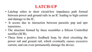
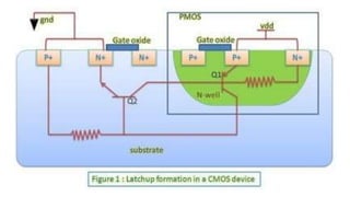
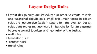
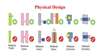
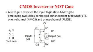
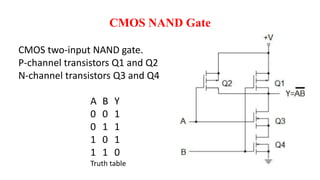
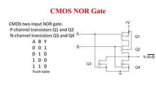
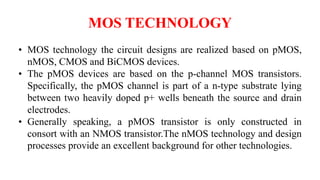
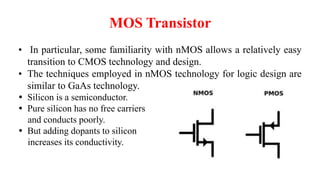
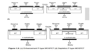
XEC607 VLSI DESIGN AND EMBEDDED
SYSTEMS
UNIT I - CMOS TECHNOLOGY
Bipolar Transistor
LATCH-UP
• Latchup refers to short circuit/low impedance path formed
between power and ground rails in an IC leading to high current
and damage to the IC.
• It occurs due to interaction between parasitic pnp and npn
transistors.
• The structure formed by these resembles a Silicon Controlled
rectifier (SCR).
• These form a positive feedback loop, by short circuiting the
power rail and ground rail, which eventually causes excessive
current, and can even permanently damage the device.
Latch-up Prevention
• 1) Putting a high resistance in the path so as to limit the
current through supply and make β1 *β2 < 1.
• 2) Surrounding PMOS and NMOS transistors with an insulating
oxide layer (trench). This breaks parasitic SCR structure.
• 3) Latchup Protection Technology circuitry which shuts off the
device when latchup is detected.
Layout Design Rules
• Layout design rules are introduced in order to create reliable
and functional circuits on a small area. Main terms in design
rules are feature size (width), separation and overlap. Design
rules does represent geometric limitations for for an engineer
to create correct topology and geometry of the design.
• well rules
• transistor rules
• contact rules
• metal rules
Physical Design
CMOS Inverter or NOT Gate
• A NOT gate reverses the input logic state.A NOT gate
employing two series-connected enhancement-type MOSFETS,
one n-channel (NMOS) and one p-channel (PMOS).
A Y
0 1
1 0
Truth table
CMOS NAND Gate
CMOS two-input NAND gate.
P-channel transistors Q1 and Q2
N-channel transistors Q3 and Q4
A B Y
0 0 1
0 1 1
1 0 1
1 1 0
Truth table
CMOS NOR Gate
CMOS two-input NOR gate.
P-channel transistors Q1 and Q2
N-channel transistors Q3 and Q4
A B Y
0 0 1
0 1 0
1 0 0
1 1 0
Truth table
MOS TECHNOLOGY
• MOS technology the circuit designs are realized based on pMOS,
nMOS, CMOS and BiCMOS devices.
• The pMOS devices are based on the p-channel MOS transistors.
Specifically, the pMOS channel is part of a n-type substrate lying
between two heavily doped p+ wells beneath the source and drain
electrodes.
• Generally speaking, a pMOS transistor is only constructed in
consort with an NMOS transistor.The nMOS technology and design
processes provide an excellent background for other technologies.
MOS Transistor
• In particular, some familiarity with nMOS allows a relatively easy
transition to CMOS technology and design.
• The techniques employed in nMOS technology for logic design are
similar to GaAs technology.
 Silicon is a semiconductor.
 Pure silicon has no free carriers
and conducts poorly.
 But adding dopants to silicon
increases its conductivity.
MOS Transistor
 A junction between p-type and n-type semiconductor forms a conduction
path. Source and Drain of the Metal Oxide Semiconductor (MOS)
 Transistor is formed by the “doped” regions on the surface of chip.
 Oxide layer is formed by means of deposition of the silicon dioxide
(SiO2) layer which forms as an insulator and is a very thin pattern.
• Gate of the MOS transistor is the thin layer of “polysilicon” used to
apply electric field to the surface of silicon between Drain and source, to
form a “channel” of electrons or holes.
 Enhancement P type
 Depletion P type
VLSI
VLSI

VLSI

  • 1.
    XEC607 VLSI DESIGNAND EMBEDDED SYSTEMS UNIT I - CMOS TECHNOLOGY
  • 6.
  • 7.
    LATCH-UP • Latchup refersto short circuit/low impedance path formed between power and ground rails in an IC leading to high current and damage to the IC. • It occurs due to interaction between parasitic pnp and npn transistors. • The structure formed by these resembles a Silicon Controlled rectifier (SCR). • These form a positive feedback loop, by short circuiting the power rail and ground rail, which eventually causes excessive current, and can even permanently damage the device.
  • 9.
    Latch-up Prevention • 1)Putting a high resistance in the path so as to limit the current through supply and make β1 *β2 < 1. • 2) Surrounding PMOS and NMOS transistors with an insulating oxide layer (trench). This breaks parasitic SCR structure. • 3) Latchup Protection Technology circuitry which shuts off the device when latchup is detected.
  • 10.
    Layout Design Rules •Layout design rules are introduced in order to create reliable and functional circuits on a small area. Main terms in design rules are feature size (width), separation and overlap. Design rules does represent geometric limitations for for an engineer to create correct topology and geometry of the design. • well rules • transistor rules • contact rules • metal rules
  • 11.
  • 12.
    CMOS Inverter orNOT Gate • A NOT gate reverses the input logic state.A NOT gate employing two series-connected enhancement-type MOSFETS, one n-channel (NMOS) and one p-channel (PMOS). A Y 0 1 1 0 Truth table
  • 13.
    CMOS NAND Gate CMOStwo-input NAND gate. P-channel transistors Q1 and Q2 N-channel transistors Q3 and Q4 A B Y 0 0 1 0 1 1 1 0 1 1 1 0 Truth table
  • 14.
    CMOS NOR Gate CMOStwo-input NOR gate. P-channel transistors Q1 and Q2 N-channel transistors Q3 and Q4 A B Y 0 0 1 0 1 0 1 0 0 1 1 0 Truth table
  • 15.
    MOS TECHNOLOGY • MOStechnology the circuit designs are realized based on pMOS, nMOS, CMOS and BiCMOS devices. • The pMOS devices are based on the p-channel MOS transistors. Specifically, the pMOS channel is part of a n-type substrate lying between two heavily doped p+ wells beneath the source and drain electrodes. • Generally speaking, a pMOS transistor is only constructed in consort with an NMOS transistor.The nMOS technology and design processes provide an excellent background for other technologies.
  • 16.
    MOS Transistor • Inparticular, some familiarity with nMOS allows a relatively easy transition to CMOS technology and design. • The techniques employed in nMOS technology for logic design are similar to GaAs technology.  Silicon is a semiconductor.  Pure silicon has no free carriers and conducts poorly.  But adding dopants to silicon increases its conductivity.
  • 17.
    MOS Transistor  Ajunction between p-type and n-type semiconductor forms a conduction path. Source and Drain of the Metal Oxide Semiconductor (MOS)  Transistor is formed by the “doped” regions on the surface of chip.  Oxide layer is formed by means of deposition of the silicon dioxide (SiO2) layer which forms as an insulator and is a very thin pattern. • Gate of the MOS transistor is the thin layer of “polysilicon” used to apply electric field to the surface of silicon between Drain and source, to form a “channel” of electrons or holes.  Enhancement P type  Depletion P type