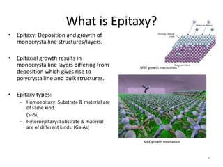
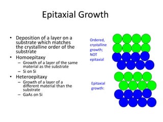
- Epitaxy involves the deposition and growth of crystalline layers on a substrate in a way that matches the substrate's crystalline structure. This results in single-crystal layers.
- Common epitaxy techniques discussed are vapor-phase epitaxy (VPE), liquid-phase epitaxy (LPE), and molecular beam epitaxy (MBE).
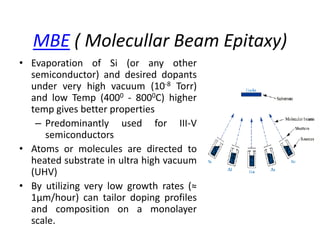
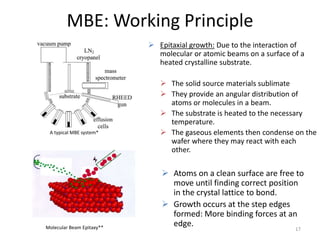
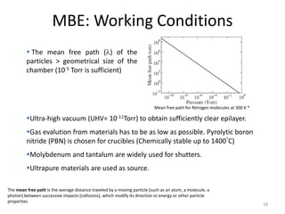
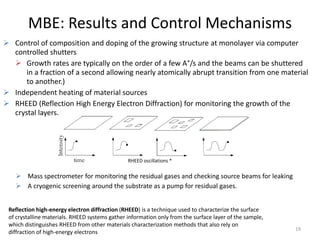
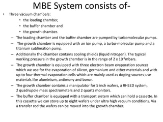
- MBE involves evaporating source materials in an ultra-high vacuum and allowing them to condense on a heated substrate. It allows precise control over composition and doping at the monolayer level.