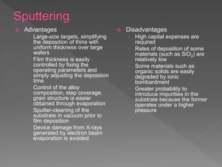
Downloaded 109 times

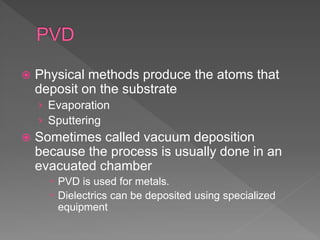
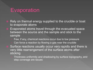
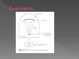
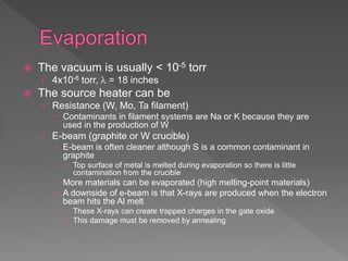
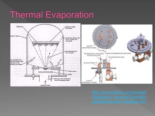
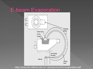
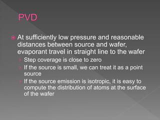
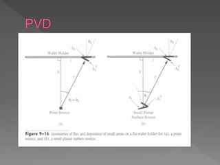
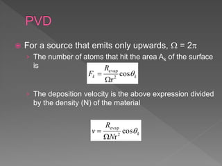
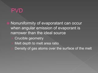
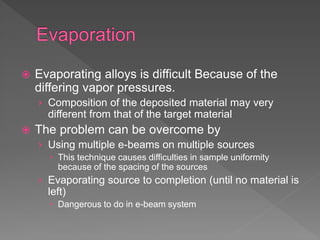
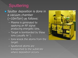
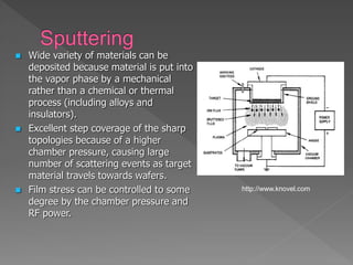

Physical vapor deposition (PVD) involves evaporating or sputtering material from a source to deposit thin films on a substrate in a vacuum chamber. In evaporation, a thermal source heats material which travels in straight lines to the substrate. Sputtering uses plasma to bombard a target, ejecting atoms which deposit with better step coverage. Both techniques can deposit a wide range of materials but sputtering provides better step coverage and evaporation risks contamination.


![Thin_Film_Technology_introduction[1]](https://cdn.slidesharecdn.com/ss_thumbnails/1b4496c8-2102-411b-8465-a3dd3f398327-150205034538-conversion-gate02-thumbnail.jpg?width=640&height=640&fit=bounds)


![Thin Film Deposition techniques [Autosaved].pptx](https://cdn.slidesharecdn.com/ss_thumbnails/thinfilmdepositionautosaved-241117063353-54857e32-thumbnail.jpg?width=640&height=640&fit=bounds)


