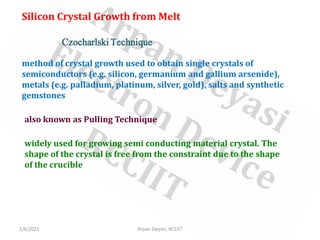
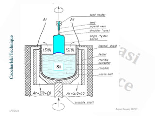
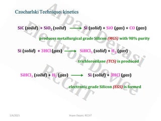
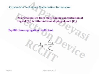
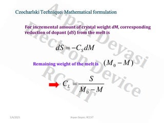
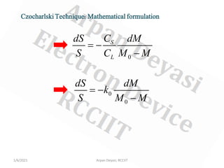
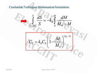
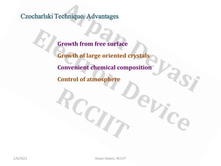
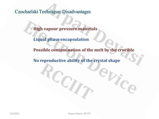
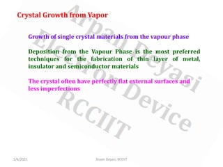
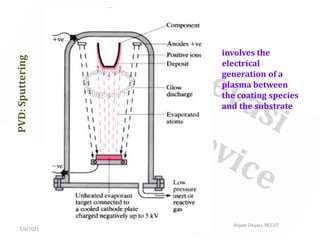
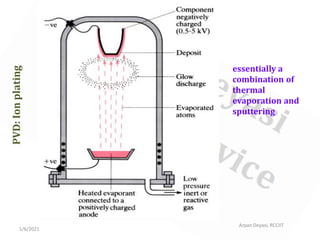
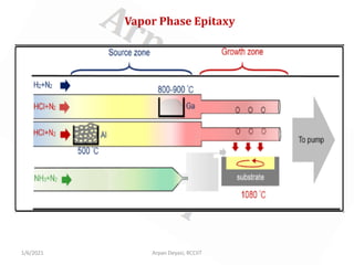
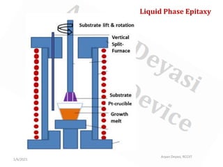
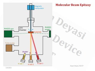
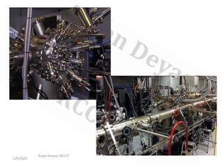
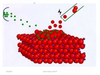
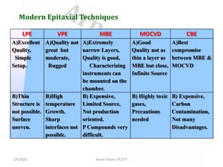
Crystal Growth
Arpan Deyasi
Dept of ECE, RCCIIT, Kolkata, India
1/6/2021 Arpan Deyasi, RCCIIT
Fabrication processes
Growth Techniques
Basic growth methods available for crystal growth
1. Growth from melt
2. Growth from vapour
3. Growth from solution
4. Growth from solid
1/6/2021 Arpan Deyasi, RCCIIT
Silicon Crystal Growth from Melt
Czocharlski Technique
method of crystal growth used to obtain single crystals of
semiconductors (e.g. silicon, germanium and gallium arsenide),
metals (e.g. palladium, platinum, silver, gold), salts and synthetic
gemstones
also known as Pulling Technique
widely used for growing semi conducting material crystal. The
shape of the crystal is free from the constraint due to the shape
of the crucible
1/6/2021
Arpan Deyasi, RCCIIT
Czocharlski
Technique
1/6/2021 Arpan Deyasi, RCCIIT
Czocharlski Technique: kinetics
SiC (solid) + SiO2 (solid) Si (solid) + SiO (gas) + CO (gas)
produces metallurgical grade Silicon (MGS) with 98% purity
Si (solid) + 3HCl(gas) SiHCl3 (solid) + H2 (gas)
trichlorosilane (TCS) is produced
SiHCl3 (solid) + H2 (gas) Si (solid) + 3HCl(gas)
electronic grade Silicon (EGS) is formed
1/6/2021 Arpan Deyasi, RCCIIT
Czocharlski Technique: Mathematical formulation
As crystal pulled from melt, doping concentration of
crystal (CS) is different from doping of melt (CL)
Equilibrium segregation coefficient
0
S
L
C
k
C
=
1/6/2021 Arpan Deyasi, RCCIIT
Czocharlski Technique: Mathematical formulation
For incremental amount of crystal weight dM, corresponding
reduction of dopant (dS) from the melt is
0
( )
M M
−
Remaining weight of the melt is
S
dS C dM
= −
0
L
S
C
M M
=
−
1/6/2021 Arpan Deyasi, RCCIIT
Czocharlski Technique: Mathematical formulation
0
S
L
C
dS dM
S C M M
= −
−
0
0
dS dM
k
S M M
= −
−
1/6/2021 Arpan Deyasi, RCCIIT
Czocharlski Technique: Mathematical formulation
0 0
0
0
0
S M
C M
dS dM
k
S M M
= −
−
∫ ∫
0
( 1)
0 0
0
1
k
S
M
C k C
M
−
 
= −
 
 
1/6/2021 Arpan Deyasi, RCCIIT
Growth from free surface
Growth of large oriented crystals
Convenient chemical composition
Control of atmosphere
Czocharlski Technique: Advantages
1/6/2021 Arpan Deyasi, RCCIIT
Czocharlski Technique: Disadvantages
High vapour pressure materials
Liquid phase encapsulation
Possible contamination of the melt by the crucible
No reproductive ability of the crystal shape
1/6/2021 Arpan Deyasi, RCCIIT
Growth of single crystal materials from the vapour phase
Deposition from the Vapour Phase is the most preferred
techniques for the fabrication of thin layer of metal,
insulator and semiconductor materials
The crystal often have perfectly flat external surfaces and
less imperfections
Crystal Growth from Vapor
1/6/2021 Arpan Deyasi, RCCIIT
Crystal Growth from Vapor
1/6/2021 Arpan Deyasi, RCCIIT
• Convenient for large large-scale operation
• Coat irregular-shaped substrates including growth on
inner surfaces
• Offer maximum control of material properties such as
thickness and composition
• Does not involve contacting of growing surface with
liquid/ solid phase
Crystal Growth from Vapor: Advantages
1/6/2021 Arpan Deyasi, RCCIIT
Physical Vapour Deposition (PVD)
Physical vapour deposition (PVD) is a thin-film coating process
which produces coatings of pure metals, metallic alloys and
ceramics with a thickness usually in the range 1 to 10µm.
Physical vapour deposition, as its name implies, involves
physically depositing atoms, ions or molecules of a coating
species on to a substrate.
• thermal evaporation
• sputtering
• ion plating
1/6/2021
Arpan Deyasi, RCCIIT
PVD:
Thermal
evaporation
uses the heating of a
material to form a
vapour which
condenses on a
substrate to form the
coating. Heating is
achieved by various
methods including
hot filament,
electrical resistance,
electron or laser
beam and electric
arc.
1/6/2021
Arpan Deyasi, RCCIIT
PVD:
Sputtering
involves the
electrical
generation of a
plasma between
the coating species
and the substrate
1/6/2021
Arpan Deyasi, RCCIIT
PVD:
Ion
plating
essentially a
combination of
thermal
evaporation and
sputtering
1/6/2021 Arpan Deyasi, RCCIIT
Advantages of PVD
Materials can be deposited with improved properties
compared to the substrate material
Almost any type of inorganic material can be used as
well as some kinds of organic materials
The process is more environmentally friendly than
processes such as electroplating
1/6/2021 Arpan Deyasi, RCCIIT
Disadvantages of PVD
It is a line of sight technique meaning that it is extremely
difficult to coat undercuts and similar surface features
High capital cost
Some processes operate at high vacuums and temperatures
requiring skilled operators
Processes requiring large amounts of heat require
appropriate cooling systems
The rate of coating deposition is usually quite slow
1/6/2021 Arpan Deyasi, RCCIIT
Chemical Vapour Deposition (CVD)
Chemical vapour deposition (CVD) is a coating process that
uses thermally induced chemical reactions at the surface of
a heated substrate, with reagents supplied in gaseous form.
These reactions may involve the substrate material itself,
but often do not.
MOCVD
enables very thin layers of atoms to be deposited on a
semiconductor wafer and is a key process for
manufacturing III-V compound semiconductors,
especially gallium nitride (GaN)-based semiconductors.
1/6/2021 Arpan Deyasi, RCCIIT
MOCVD
Epitaxial Growth
• Deposition of a layer on a
substrate which matches the
crystalline order of the
substrate
• Homo-epitaxy
– Growth of a layer of the
same material as the
substrate
– Si on Si
• Hetero-epitaxy
– Growth of a layer of a
different material than the
substrate
– GaAs on Si
Ordered,
crystalline
growth;
NOT
epitaxial
Epitaxial
growth:
Types of epitaxial deposition
• Vapor Phase Epitaxy
• Liquid Phase Epitaxy
• Molecular Beam Epitaxy
1/6/2021 Arpan Deyasi, RCCIIT
Vapor Phase Epitaxy
1/6/2021
Arpan Deyasi, RCCIIT
Liquid Phase Epitaxy
1/6/2021
Arpan Deyasi, RCCIIT
Molecular Beam Epitaxy
– Very promising technique
– Beams created by evaporating solid source in UHV
– Evaporated beam of particle travel through very high vacuum
and then condense to shape the layer
– Doping is possible to by adding impurity to source gas
– Deposition rate is the most important aspect of MBE
– Thickness of each layer can be controlled to that of a single
atom
– Development of structures where the electrons can be
confined in space, giving quantum structures
1/6/2021
Arpan Deyasi, RCCIIT
1/6/2021 Arpan Deyasi, RCCIIT
Modern Epitaxial Techniques

Crystal Growth

  • 1.
    Crystal Growth Arpan Deyasi Deptof ECE, RCCIIT, Kolkata, India 1/6/2021 Arpan Deyasi, RCCIIT
  • 2.
    1/6/2021 Arpan Deyasi,RCCIIT Fabrication processes Growth Techniques Basic growth methods available for crystal growth 1. Growth from melt 2. Growth from vapour 3. Growth from solution 4. Growth from solid
  • 3.
    1/6/2021 Arpan Deyasi,RCCIIT Silicon Crystal Growth from Melt Czocharlski Technique method of crystal growth used to obtain single crystals of semiconductors (e.g. silicon, germanium and gallium arsenide), metals (e.g. palladium, platinum, silver, gold), salts and synthetic gemstones also known as Pulling Technique widely used for growing semi conducting material crystal. The shape of the crystal is free from the constraint due to the shape of the crucible
  • 4.
  • 5.
    1/6/2021 Arpan Deyasi,RCCIIT Czocharlski Technique: kinetics SiC (solid) + SiO2 (solid) Si (solid) + SiO (gas) + CO (gas) produces metallurgical grade Silicon (MGS) with 98% purity Si (solid) + 3HCl(gas) SiHCl3 (solid) + H2 (gas) trichlorosilane (TCS) is produced SiHCl3 (solid) + H2 (gas) Si (solid) + 3HCl(gas) electronic grade Silicon (EGS) is formed
  • 6.
    1/6/2021 Arpan Deyasi,RCCIIT Czocharlski Technique: Mathematical formulation As crystal pulled from melt, doping concentration of crystal (CS) is different from doping of melt (CL) Equilibrium segregation coefficient 0 S L C k C =
  • 7.
    1/6/2021 Arpan Deyasi,RCCIIT Czocharlski Technique: Mathematical formulation For incremental amount of crystal weight dM, corresponding reduction of dopant (dS) from the melt is 0 ( ) M M − Remaining weight of the melt is S dS C dM = − 0 L S C M M = −
  • 8.
    1/6/2021 Arpan Deyasi,RCCIIT Czocharlski Technique: Mathematical formulation 0 S L C dS dM S C M M = − − 0 0 dS dM k S M M = − −
  • 9.
    1/6/2021 Arpan Deyasi,RCCIIT Czocharlski Technique: Mathematical formulation 0 0 0 0 0 S M C M dS dM k S M M = − − ∫ ∫ 0 ( 1) 0 0 0 1 k S M C k C M −   = −    
  • 10.
    1/6/2021 Arpan Deyasi,RCCIIT Growth from free surface Growth of large oriented crystals Convenient chemical composition Control of atmosphere Czocharlski Technique: Advantages
  • 11.
    1/6/2021 Arpan Deyasi,RCCIIT Czocharlski Technique: Disadvantages High vapour pressure materials Liquid phase encapsulation Possible contamination of the melt by the crucible No reproductive ability of the crystal shape
  • 12.
    1/6/2021 Arpan Deyasi,RCCIIT Growth of single crystal materials from the vapour phase Deposition from the Vapour Phase is the most preferred techniques for the fabrication of thin layer of metal, insulator and semiconductor materials The crystal often have perfectly flat external surfaces and less imperfections Crystal Growth from Vapor
  • 13.
    1/6/2021 Arpan Deyasi,RCCIIT Crystal Growth from Vapor
  • 14.
    1/6/2021 Arpan Deyasi,RCCIIT • Convenient for large large-scale operation • Coat irregular-shaped substrates including growth on inner surfaces • Offer maximum control of material properties such as thickness and composition • Does not involve contacting of growing surface with liquid/ solid phase Crystal Growth from Vapor: Advantages
  • 15.
    1/6/2021 Arpan Deyasi,RCCIIT Physical Vapour Deposition (PVD) Physical vapour deposition (PVD) is a thin-film coating process which produces coatings of pure metals, metallic alloys and ceramics with a thickness usually in the range 1 to 10µm. Physical vapour deposition, as its name implies, involves physically depositing atoms, ions or molecules of a coating species on to a substrate. • thermal evaporation • sputtering • ion plating
  • 16.
    1/6/2021 Arpan Deyasi, RCCIIT PVD: Thermal evaporation usesthe heating of a material to form a vapour which condenses on a substrate to form the coating. Heating is achieved by various methods including hot filament, electrical resistance, electron or laser beam and electric arc.
  • 17.
    1/6/2021 Arpan Deyasi, RCCIIT PVD: Sputtering involvesthe electrical generation of a plasma between the coating species and the substrate
  • 18.
    1/6/2021 Arpan Deyasi, RCCIIT PVD: Ion plating essentiallya combination of thermal evaporation and sputtering
  • 19.
    1/6/2021 Arpan Deyasi,RCCIIT Advantages of PVD Materials can be deposited with improved properties compared to the substrate material Almost any type of inorganic material can be used as well as some kinds of organic materials The process is more environmentally friendly than processes such as electroplating
  • 20.
    1/6/2021 Arpan Deyasi,RCCIIT Disadvantages of PVD It is a line of sight technique meaning that it is extremely difficult to coat undercuts and similar surface features High capital cost Some processes operate at high vacuums and temperatures requiring skilled operators Processes requiring large amounts of heat require appropriate cooling systems The rate of coating deposition is usually quite slow
  • 21.
    1/6/2021 Arpan Deyasi,RCCIIT Chemical Vapour Deposition (CVD) Chemical vapour deposition (CVD) is a coating process that uses thermally induced chemical reactions at the surface of a heated substrate, with reagents supplied in gaseous form. These reactions may involve the substrate material itself, but often do not. MOCVD enables very thin layers of atoms to be deposited on a semiconductor wafer and is a key process for manufacturing III-V compound semiconductors, especially gallium nitride (GaN)-based semiconductors.
  • 22.
  • 23.
    Epitaxial Growth • Depositionof a layer on a substrate which matches the crystalline order of the substrate • Homo-epitaxy – Growth of a layer of the same material as the substrate – Si on Si • Hetero-epitaxy – Growth of a layer of a different material than the substrate – GaAs on Si Ordered, crystalline growth; NOT epitaxial Epitaxial growth:
  • 24.
    Types of epitaxialdeposition • Vapor Phase Epitaxy • Liquid Phase Epitaxy • Molecular Beam Epitaxy
  • 25.
    1/6/2021 Arpan Deyasi,RCCIIT Vapor Phase Epitaxy
  • 26.
  • 27.
  • 28.
    Molecular Beam Epitaxy –Very promising technique – Beams created by evaporating solid source in UHV – Evaporated beam of particle travel through very high vacuum and then condense to shape the layer – Doping is possible to by adding impurity to source gas – Deposition rate is the most important aspect of MBE – Thickness of each layer can be controlled to that of a single atom – Development of structures where the electrons can be confined in space, giving quantum structures
  • 29.
  • 30.
  • 31.
    1/6/2021 Arpan Deyasi,RCCIIT Modern Epitaxial Techniques