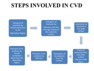
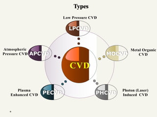
CHEMICAL VAPOUR DEPOSITION
Basic Process
DEPOSITION
• Chemical deposition :
Chemical deposition techniques include chemical
vapor deposition , in which a stream of source gas
reacts on the substrate to grow the material desired.
• Physical deposition :
Physical deposition consists of a process in which a
material is removed from a target, and deposited on a
surface.
CHEMICAL VAPOUR DEPOSITION
• Chemical Vapour Deposition (CVD) is a chemical
process used to produce high purity, high performance
solid materials.
• In a typical CVD process, the substrate is exposed to
one or more volatile precursors which react and
decompose on the substrate surface to produce the
desired deposit.
• During this process, volatile by-products are also
produced, which are removed by gas flow through the
reaction chamber.
STEPS INVOLVED IN CVD
Transport of
reactants by
forced convection
to the
Deposition Region
Transport of
reactants by
Diffusion from the
main gas stream to
the substrate
surface.
Adsorption of
reactants in
the wafer
surface.
Chemical
decomposition
and other
surface
reactions take
place.
Desorption of
by-products
from the
surface.
Transport of by-
products by
diffusion
Transport of by-
products by
forced
convection
away from the
deposition
region.
Types
Low Pressure CVD
LPCVD
Atmospheric
Pressure CVD
Metal Organic
CVDAPCVD MOCVD
CVD
Plasma
Enhanced CVD
Photon (Laser)
Induced CVDPECVD PHCVD
●CVD at different operating pressures (APCVD; SACVD;
LPCVD; UHV/CVD)
●Plasma-enhanced CVD (PECVD)
●Metal-organic CVD (MOCVD)
Types of CVD processes
● Atmospheric pressure CVD (APCVD)
● Sub-atmospheric pressure CVD (SACVD)
● 1000 mbar > P > 10 mbar
● Reduction of unwanted gas phase reactions
● Improvement of film uniformity across the wafer
● Low-pressure CVD (LPCVD)
● 1 mbar > P > 0.1 mbar
● Ultrahigh vacuum CVD (UHV/CVD)
● Initial vacuum of 10-7 - 10-8 mbar; growth at P 10-3 mbar
● No gas phase reactions
● No gas boundary layer near wafer surface, but molecular flow
transport
Classification of CVD by pressure
Atmospheric pressure CVD (APCVD)
● High pressure results in fast film growth rates
(micron/minute)
● High gas consumption
● Also carrier or diluent gas can be used (e.g. N2 or
H2)
● 350 ºC < T < 1200 ºC
● Growth of oxides at low temperatures
● At high temperature, growth is in the mass transport-
limited regime  gas flow control is very important
● Wafer is placed horizontally in the gas flow  limits
throughput
● Reaction may already start in the gas phase, resulting in unwanted precipitates
on the wafer non- uniformities or pinholes in deposited film
● Reduced gas consumption
● More uniform films grown
● No particle formation
● Wafers still horizontally placed
low throughput
Sub-atmospheric pressure CVD (SACVD)
Wafer
1000 mbar > P > 10 mbar
Wafer
Heater
Low-pressure CVD (LPCVD)
● Low pressure results in increased gas
diffusion
● No gas concentration gradient
perpendicular to flow direction
● More uniform films
● 400 ºC < T < 900 ºC
● Growth in reaction-limited regime
● Precise temperature control is important
● Wafers can be stacked vertically in batches due to homogeneous gas conditions 
wafer throughput can be enhanced
● Downstream depletion of gases can be compensated by establishing a temperature
gradient in the heater system
● Molecular mean free path is of
the order of the chamber
dimension
● No gas boundary layer effects
near wafer surface, only
molecular flow
● No gas-phase chemical reactions
● 500 ºC < T < 600 ºC
● Low partial pressure of
contaminant gases
enables low-temperature growth
with minimum thermal budget-
related dopant diffusion in
semiconductors
Ultrahigh vacuum CVD (UHV/CVD)
Heater
Initial vacuum 10-7 - 10-8 mbar
Deposition at P 10-3 mbar
Wafer Heater
● Based on LPCVD-like
configuration
● Radio Frequency (RF) power
coupled into the gas, typically at
400 kHz or 13.56 MHz
● RF power induces plasma, i.e. a
partially ionized gas, containing
ions, electrons and excited gas
molecules
Plasma-enhanced CVD (PECVD)
Wafer
Plasm
a
Wafer
He ter
a
R
F
● Film growth is in the reaction-
limited regime
Plasma-enhanced CVD (PECVD)
𝑡 𝑓ilm x ~
−
𝐸 𝑎ctiv
𝑘 𝐵 𝑇
𝐸 𝑎ctiv
F
W
F
F
F
F
F
W
No
plasma
e
● Film growth is in the reaction-
limited regime
● Plasma raises all molecular
energies
● Effective activation energy is
reduced
● Increased growth rate possible
● Growth becomes possible at
lower temperature  less
restrictions to the used
substrate
Plasma-enhanced CVD (PECVD)
𝑡 𝑓ilm 𝑥 ~
−
𝐸 𝑎ctiv
𝑘 𝐵 𝑇
𝐸 𝑎𝑎𝑎
𝑓𝑎
F
W
F
F
F
F
F
W
RF plasma
e
● Also called “metal-organic
vapour phase epitaxy (MOVPE)”
● Transport of volatile metal-
organic precursor molecules by
a carrier gas (H2 or N2) that
bubbles through the precursor
liquid
Metal-organic CVD (MOCVD)
Wafer
1000 mbar > P > 10 mbar
Wafer
Heater
H2
in
precursor
molecules out
liquid precursor
thermal bath
● Surface reaction of metal-
organic compounds (liquid
precursors) and hydrides
(gaseous precursors) allows
deposition of compound
semiconductors, e.g. GaAs or
InP
● 300 ºC < T < 500 ºC
● Vapour pressure control of
metal- organic source critical
● Safety aspects important
Metal-organic CVD (MOCVD)
● Atomic layer CVD (ALCVD)
● Thermal oxidation (not truly a CVD process)
CVD processes
● Process is repeated generating a sequence of layers
● Technique to produce very thin, atomically specified conformal films
● Reaction is self-limiting, i.e. it stops once all reactive sites on the
surface of the wafer are occupied
● Example: trimethyl aluminium [Al(CH3)3] and H2O vapour exposure
sequences to form very thin and continuous Al2O3 dielectric films
Atomic layer CVD (ALCVD)
● Individual application of two
reactant gases A and B
allowing sequential
formation of layers
● Each of the
two
reaction steps is self-limiting
 one molecular monolayer
deposition at a time
● SiO2 is an extremely important material in
silicon technology
● Thin oxides (1-20 nm) are used as dielectric
in transistors
● Thick oxides (100-1000 nm) serve as
protective coatings and for electrical
isolation
● In thermal oxidation, silicon is transformed
into its oxide at high temperature (850 ºC < T
< 1100 ºC) using either water vapor (“wet
oxidation”) or oxygen (“dry oxidation”).
● Water vapor is produced by
combustion of H2 and O2 in a torch
Thermal oxidation
𝑆i(s) + 2 H2O (g) => SiO2 (S) + 2H2 (g)
𝑆i(s) + O2 (g) => SiO2 (S)
Thermal oxidation mechanism
● SiO2 is formed by diffusion of oxygen into
the Si wafer
● Oxidation is at the SiO2/Si interface
● Initially oxide thickness 𝑡 𝑜x~𝑡ime,
later 𝑡 𝑜x~ time due to increased diffusion
length
● Slow process
● Wet @ 900 ºC : 130 nm in 1 hour
● Dry @ 900 ºC : 30 nm in 1 hour
● Incorporation of oxygen increases thevolume: 𝑡
𝑜x replaces a Si thickness of 0.45 𝑡 𝑜x
Deposition of wet thermal oxide
•Wet oxidation (using H2O vapour)
allows fast transformation of the
surface of a Si wafer, layers of
poly-Si into oxide
•Thick layers (up to 2 μm) can be
realized
•Such oxide layers can be used e.g.
as protective masking layer in
plasma etching, or used as thick
electrical insulation layers in
microelectronic circuits (LOCOS
process)
Deposition of wet thermal oxide
1. Fused silica tube
2. Heating elements (3 zones)
3. Fused silica seal
4. Three fused silica boats, each for 25
wafers of 100 mm or 150 mm Ø
5. Temperature sensor
6. Hydrogen gas (H2) entrance
7. Oxygen gas (O2) entrance
8. Hydrogen torch system: H2 and O2 are
mixed at temperatures above about 600 ºC.
This produces a controlled combustion
which reaches temperatures of about 1200 ºC
whereby water vapor is formed.
9. Nitrogen gas (N2) entrance
Deposition of Dry thermal oxide
•Dry thermal oxidation is used for
realisation of the thin gate oxide
layer in MOS transistors
•A dichloroethylene (C 2H2Cl2 )
bubbler allows controlled growth of
ultrathin oxides (20-25 nm)
•C2H2Cl2 is a liquid source that
generates high-purity HCl, which
reacts with metal contaminants so
that a high-quality low-defect thin
oxide can be grown
𝐶𝐻2 𝐶l2+ 2𝑂2 → 2 𝐻Cl + 2 𝐶O2
Deposition of Dry thermal oxide
1. Fused silica tube
2. Heating elements (3 zones)
3. Fused silica seal
4. Three fused silica boats, each for
25 wafers of 100 mm or 150 mm Ø
5. Temperature sensor
6. Oxygen gas (O2) entrance
7. Nitrogen gas (N2) entrance
8. Dichloroethylene (DCE)
(C2H2Cl2) bubbler
9. Nitrogen gas (N2) -
dichloroethylene (C2H2 Cl2)
entrance
Classification of CVD by reactor type
1.Hot wall tube reactor
•Wafers are placed in a fused
silica boat that is inserted in a
fused silica tube
• Whole system is heated
Uniform temperature
Possible deposition on walls
Classification of CVD by reactor type
2.Cold wall tube reactor
• Wafers are placed on a graphite susceptor that is tilted
to reduce downstream depletion of the gas
•Graphite with wafers is inductively heated
 Locally high temperature and gradient
 No deposition on walls
Classification of CVD by reactor type
3.Showerhead reactor 4.Conveyor belt reactor
• Wafer is placed on a local
heater
• ‘Shower’ of gas exposes
the wafer
• Wafers are placed on
transport belt situated above
a local heater
• Increased wafer throughput
Theoretical concepts in CVD
•Velocity boundary layer near a substrate
•Concentration boundary layer near a heated substrate
Velocity boundary layer near a substrate
•Gas flowing over a surface
at y=0 velocity in the y-
direction varies from 0 to
value u∞ at infinity
•Development of
hydrodynamic or velocity
boundary layer
•If temperature gradient,
development of thermal
boundary layer
•Boundary layer grows as
flow progresses in the x
direction
Velocity boundary layer near a substrate
• Retardation of fluid motion
associated with shear stresses τ
acting in planes parallel to the
fluid velocity
• δ(x) : boundary layer thickness,
defined as value for y for which
u(y) = 0.99 u∞
• Boundary layer grows with x, as
effects of viscosity penetrate
further in the gas stream
• Two distinct regions in fluid flow:
(i) boundary layer where velocity
gradients and shear stresses are
large; (ii) the region outside,
where these are negligible
Concentration boundary layer near heated
substrate
•Gas flows over the wafer
surface and is transformed in a
solid reaction product
•The gas stream thereby is
gradually depleted and a gas
concentration gradient ρ(y,x)
develops in the boundary layer
•Renewal of the gas from the
free stream towards the
substrate occurs by diffusion
Laminar and turbulent flow
•In general, the boundary layer can be
laminar or turbulent
•Laminar
• fluid motion is highly ordered
• clear streamlines
• presence of velocity component v
necessitated by boundary layer growth in
x direction
•Turbulent
• irregular flow with velocity fluctuations
• increased surface friction and turbulent
mixing
•CVD is normally operated in the laminar
flow boundary layer regime
Advantages
 CVD films are generally quite conformal, i.e., the ability of a
film to uniformly coat a topographically complex substrate.
 Versatile –any element or compound can be deposited.
 High purity can be obtained.
 High density – nearly 100% of theoretical value.
 CVD films are harder than similar materials produced using
conventional ceramic fabrication processes.
 Material formation well below the melting point.
 Economical in production, since many parts can be coated
at the same time.
Applications
 Coatings – Coatings for a variety of applications such as
wear resistance, corrosion resistance, high temperature
protection.
 Semiconductors and related devices – Integrated circuits,
sensors and optoelectronic devices.
 Fiber optics – for telecommunication.
 Used in the microelectronics industry to make films
serving as dielectrics, conductors, passivation layers,
oxidation barriers, and epitaxial layers.
THANK YOU

Cvd

  • 1.
  • 2.
  • 3.
    DEPOSITION • Chemical deposition: Chemical deposition techniques include chemical vapor deposition , in which a stream of source gas reacts on the substrate to grow the material desired. • Physical deposition : Physical deposition consists of a process in which a material is removed from a target, and deposited on a surface.
  • 4.
    CHEMICAL VAPOUR DEPOSITION •Chemical Vapour Deposition (CVD) is a chemical process used to produce high purity, high performance solid materials. • In a typical CVD process, the substrate is exposed to one or more volatile precursors which react and decompose on the substrate surface to produce the desired deposit. • During this process, volatile by-products are also produced, which are removed by gas flow through the reaction chamber.
  • 5.
    STEPS INVOLVED INCVD Transport of reactants by forced convection to the Deposition Region Transport of reactants by Diffusion from the main gas stream to the substrate surface. Adsorption of reactants in the wafer surface. Chemical decomposition and other surface reactions take place. Desorption of by-products from the surface. Transport of by- products by diffusion Transport of by- products by forced convection away from the deposition region.
  • 6.
    Types Low Pressure CVD LPCVD Atmospheric PressureCVD Metal Organic CVDAPCVD MOCVD CVD Plasma Enhanced CVD Photon (Laser) Induced CVDPECVD PHCVD
  • 7.
    ●CVD at differentoperating pressures (APCVD; SACVD; LPCVD; UHV/CVD) ●Plasma-enhanced CVD (PECVD) ●Metal-organic CVD (MOCVD) Types of CVD processes
  • 8.
    ● Atmospheric pressureCVD (APCVD) ● Sub-atmospheric pressure CVD (SACVD) ● 1000 mbar > P > 10 mbar ● Reduction of unwanted gas phase reactions ● Improvement of film uniformity across the wafer ● Low-pressure CVD (LPCVD) ● 1 mbar > P > 0.1 mbar ● Ultrahigh vacuum CVD (UHV/CVD) ● Initial vacuum of 10-7 - 10-8 mbar; growth at P 10-3 mbar ● No gas phase reactions ● No gas boundary layer near wafer surface, but molecular flow transport Classification of CVD by pressure
  • 9.
    Atmospheric pressure CVD(APCVD) ● High pressure results in fast film growth rates (micron/minute) ● High gas consumption ● Also carrier or diluent gas can be used (e.g. N2 or H2) ● 350 ºC < T < 1200 ºC ● Growth of oxides at low temperatures ● At high temperature, growth is in the mass transport- limited regime  gas flow control is very important ● Wafer is placed horizontally in the gas flow  limits throughput ● Reaction may already start in the gas phase, resulting in unwanted precipitates on the wafer non- uniformities or pinholes in deposited film
  • 10.
    ● Reduced gasconsumption ● More uniform films grown ● No particle formation ● Wafers still horizontally placed low throughput Sub-atmospheric pressure CVD (SACVD) Wafer 1000 mbar > P > 10 mbar Wafer Heater
  • 11.
    Low-pressure CVD (LPCVD) ●Low pressure results in increased gas diffusion ● No gas concentration gradient perpendicular to flow direction ● More uniform films ● 400 ºC < T < 900 ºC ● Growth in reaction-limited regime ● Precise temperature control is important ● Wafers can be stacked vertically in batches due to homogeneous gas conditions  wafer throughput can be enhanced ● Downstream depletion of gases can be compensated by establishing a temperature gradient in the heater system
  • 12.
    ● Molecular meanfree path is of the order of the chamber dimension ● No gas boundary layer effects near wafer surface, only molecular flow ● No gas-phase chemical reactions ● 500 ºC < T < 600 ºC ● Low partial pressure of contaminant gases enables low-temperature growth with minimum thermal budget- related dopant diffusion in semiconductors Ultrahigh vacuum CVD (UHV/CVD) Heater Initial vacuum 10-7 - 10-8 mbar Deposition at P 10-3 mbar Wafer Heater
  • 13.
    ● Based onLPCVD-like configuration ● Radio Frequency (RF) power coupled into the gas, typically at 400 kHz or 13.56 MHz ● RF power induces plasma, i.e. a partially ionized gas, containing ions, electrons and excited gas molecules Plasma-enhanced CVD (PECVD) Wafer Plasm a Wafer He ter a R F
  • 14.
    ● Film growthis in the reaction- limited regime Plasma-enhanced CVD (PECVD) 𝑡 𝑓ilm x ~ − 𝐸 𝑎ctiv 𝑘 𝐵 𝑇 𝐸 𝑎ctiv F W F F F F F W No plasma e
  • 15.
    ● Film growthis in the reaction- limited regime ● Plasma raises all molecular energies ● Effective activation energy is reduced ● Increased growth rate possible ● Growth becomes possible at lower temperature  less restrictions to the used substrate Plasma-enhanced CVD (PECVD) 𝑡 𝑓ilm 𝑥 ~ − 𝐸 𝑎ctiv 𝑘 𝐵 𝑇 𝐸 𝑎𝑎𝑎 𝑓𝑎 F W F F F F F W RF plasma e
  • 16.
    ● Also called“metal-organic vapour phase epitaxy (MOVPE)” ● Transport of volatile metal- organic precursor molecules by a carrier gas (H2 or N2) that bubbles through the precursor liquid Metal-organic CVD (MOCVD) Wafer 1000 mbar > P > 10 mbar Wafer Heater H2 in precursor molecules out liquid precursor thermal bath
  • 17.
    ● Surface reactionof metal- organic compounds (liquid precursors) and hydrides (gaseous precursors) allows deposition of compound semiconductors, e.g. GaAs or InP ● 300 ºC < T < 500 ºC ● Vapour pressure control of metal- organic source critical ● Safety aspects important Metal-organic CVD (MOCVD)
  • 18.
    ● Atomic layerCVD (ALCVD) ● Thermal oxidation (not truly a CVD process) CVD processes
  • 19.
    ● Process isrepeated generating a sequence of layers ● Technique to produce very thin, atomically specified conformal films ● Reaction is self-limiting, i.e. it stops once all reactive sites on the surface of the wafer are occupied ● Example: trimethyl aluminium [Al(CH3)3] and H2O vapour exposure sequences to form very thin and continuous Al2O3 dielectric films Atomic layer CVD (ALCVD) ● Individual application of two reactant gases A and B allowing sequential formation of layers ● Each of the two reaction steps is self-limiting  one molecular monolayer deposition at a time
  • 20.
    ● SiO2 isan extremely important material in silicon technology ● Thin oxides (1-20 nm) are used as dielectric in transistors ● Thick oxides (100-1000 nm) serve as protective coatings and for electrical isolation ● In thermal oxidation, silicon is transformed into its oxide at high temperature (850 ºC < T < 1100 ºC) using either water vapor (“wet oxidation”) or oxygen (“dry oxidation”). ● Water vapor is produced by combustion of H2 and O2 in a torch Thermal oxidation 𝑆i(s) + 2 H2O (g) => SiO2 (S) + 2H2 (g) 𝑆i(s) + O2 (g) => SiO2 (S)
  • 21.
    Thermal oxidation mechanism ●SiO2 is formed by diffusion of oxygen into the Si wafer ● Oxidation is at the SiO2/Si interface ● Initially oxide thickness 𝑡 𝑜x~𝑡ime, later 𝑡 𝑜x~ time due to increased diffusion length ● Slow process ● Wet @ 900 ºC : 130 nm in 1 hour ● Dry @ 900 ºC : 30 nm in 1 hour ● Incorporation of oxygen increases thevolume: 𝑡 𝑜x replaces a Si thickness of 0.45 𝑡 𝑜x
  • 22.
    Deposition of wetthermal oxide •Wet oxidation (using H2O vapour) allows fast transformation of the surface of a Si wafer, layers of poly-Si into oxide •Thick layers (up to 2 μm) can be realized •Such oxide layers can be used e.g. as protective masking layer in plasma etching, or used as thick electrical insulation layers in microelectronic circuits (LOCOS process)
  • 23.
    Deposition of wetthermal oxide 1. Fused silica tube 2. Heating elements (3 zones) 3. Fused silica seal 4. Three fused silica boats, each for 25 wafers of 100 mm or 150 mm Ø 5. Temperature sensor 6. Hydrogen gas (H2) entrance 7. Oxygen gas (O2) entrance 8. Hydrogen torch system: H2 and O2 are mixed at temperatures above about 600 ºC. This produces a controlled combustion which reaches temperatures of about 1200 ºC whereby water vapor is formed. 9. Nitrogen gas (N2) entrance
  • 24.
    Deposition of Drythermal oxide •Dry thermal oxidation is used for realisation of the thin gate oxide layer in MOS transistors •A dichloroethylene (C 2H2Cl2 ) bubbler allows controlled growth of ultrathin oxides (20-25 nm) •C2H2Cl2 is a liquid source that generates high-purity HCl, which reacts with metal contaminants so that a high-quality low-defect thin oxide can be grown 𝐶𝐻2 𝐶l2+ 2𝑂2 → 2 𝐻Cl + 2 𝐶O2
  • 25.
    Deposition of Drythermal oxide 1. Fused silica tube 2. Heating elements (3 zones) 3. Fused silica seal 4. Three fused silica boats, each for 25 wafers of 100 mm or 150 mm Ø 5. Temperature sensor 6. Oxygen gas (O2) entrance 7. Nitrogen gas (N2) entrance 8. Dichloroethylene (DCE) (C2H2Cl2) bubbler 9. Nitrogen gas (N2) - dichloroethylene (C2H2 Cl2) entrance
  • 26.
    Classification of CVDby reactor type 1.Hot wall tube reactor •Wafers are placed in a fused silica boat that is inserted in a fused silica tube • Whole system is heated Uniform temperature Possible deposition on walls
  • 27.
    Classification of CVDby reactor type 2.Cold wall tube reactor • Wafers are placed on a graphite susceptor that is tilted to reduce downstream depletion of the gas •Graphite with wafers is inductively heated  Locally high temperature and gradient  No deposition on walls
  • 28.
    Classification of CVDby reactor type 3.Showerhead reactor 4.Conveyor belt reactor • Wafer is placed on a local heater • ‘Shower’ of gas exposes the wafer • Wafers are placed on transport belt situated above a local heater • Increased wafer throughput
  • 29.
    Theoretical concepts inCVD •Velocity boundary layer near a substrate •Concentration boundary layer near a heated substrate
  • 30.
    Velocity boundary layernear a substrate •Gas flowing over a surface at y=0 velocity in the y- direction varies from 0 to value u∞ at infinity •Development of hydrodynamic or velocity boundary layer •If temperature gradient, development of thermal boundary layer •Boundary layer grows as flow progresses in the x direction
  • 31.
    Velocity boundary layernear a substrate • Retardation of fluid motion associated with shear stresses τ acting in planes parallel to the fluid velocity • δ(x) : boundary layer thickness, defined as value for y for which u(y) = 0.99 u∞ • Boundary layer grows with x, as effects of viscosity penetrate further in the gas stream • Two distinct regions in fluid flow: (i) boundary layer where velocity gradients and shear stresses are large; (ii) the region outside, where these are negligible
  • 32.
    Concentration boundary layernear heated substrate •Gas flows over the wafer surface and is transformed in a solid reaction product •The gas stream thereby is gradually depleted and a gas concentration gradient ρ(y,x) develops in the boundary layer •Renewal of the gas from the free stream towards the substrate occurs by diffusion
  • 33.
    Laminar and turbulentflow •In general, the boundary layer can be laminar or turbulent •Laminar • fluid motion is highly ordered • clear streamlines • presence of velocity component v necessitated by boundary layer growth in x direction •Turbulent • irregular flow with velocity fluctuations • increased surface friction and turbulent mixing •CVD is normally operated in the laminar flow boundary layer regime
  • 34.
    Advantages  CVD filmsare generally quite conformal, i.e., the ability of a film to uniformly coat a topographically complex substrate.  Versatile –any element or compound can be deposited.  High purity can be obtained.  High density – nearly 100% of theoretical value.  CVD films are harder than similar materials produced using conventional ceramic fabrication processes.  Material formation well below the melting point.  Economical in production, since many parts can be coated at the same time.
  • 35.
    Applications  Coatings –Coatings for a variety of applications such as wear resistance, corrosion resistance, high temperature protection.  Semiconductors and related devices – Integrated circuits, sensors and optoelectronic devices.  Fiber optics – for telecommunication.  Used in the microelectronics industry to make films serving as dielectrics, conductors, passivation layers, oxidation barriers, and epitaxial layers.
  • 36.