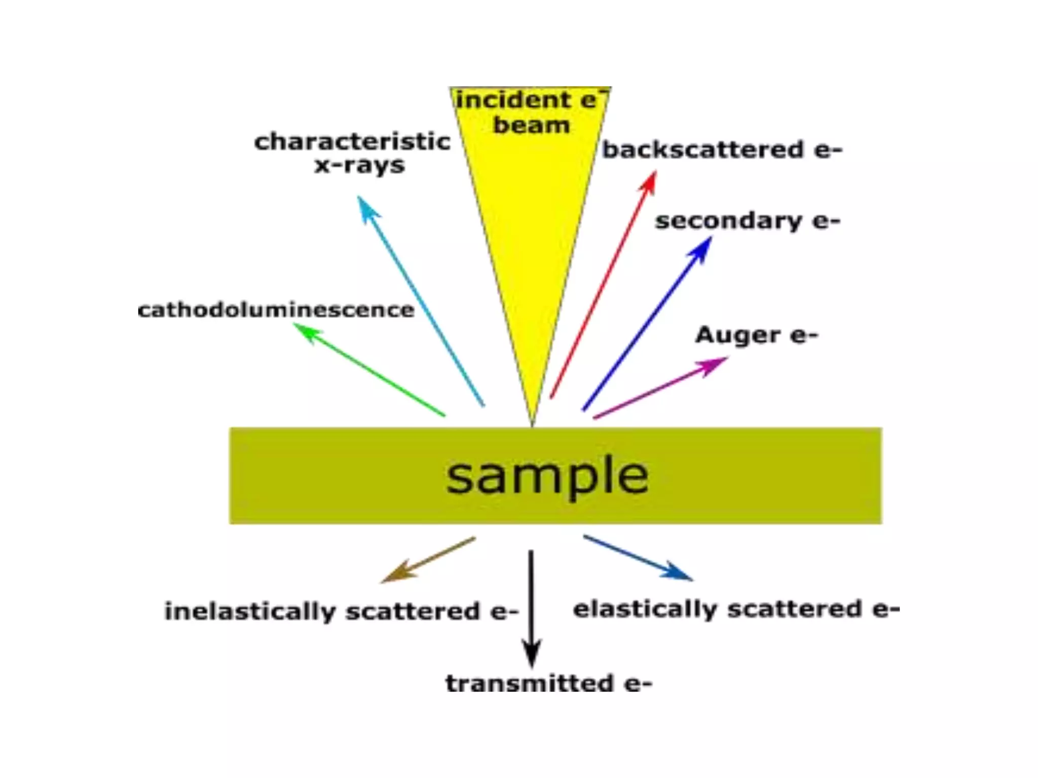
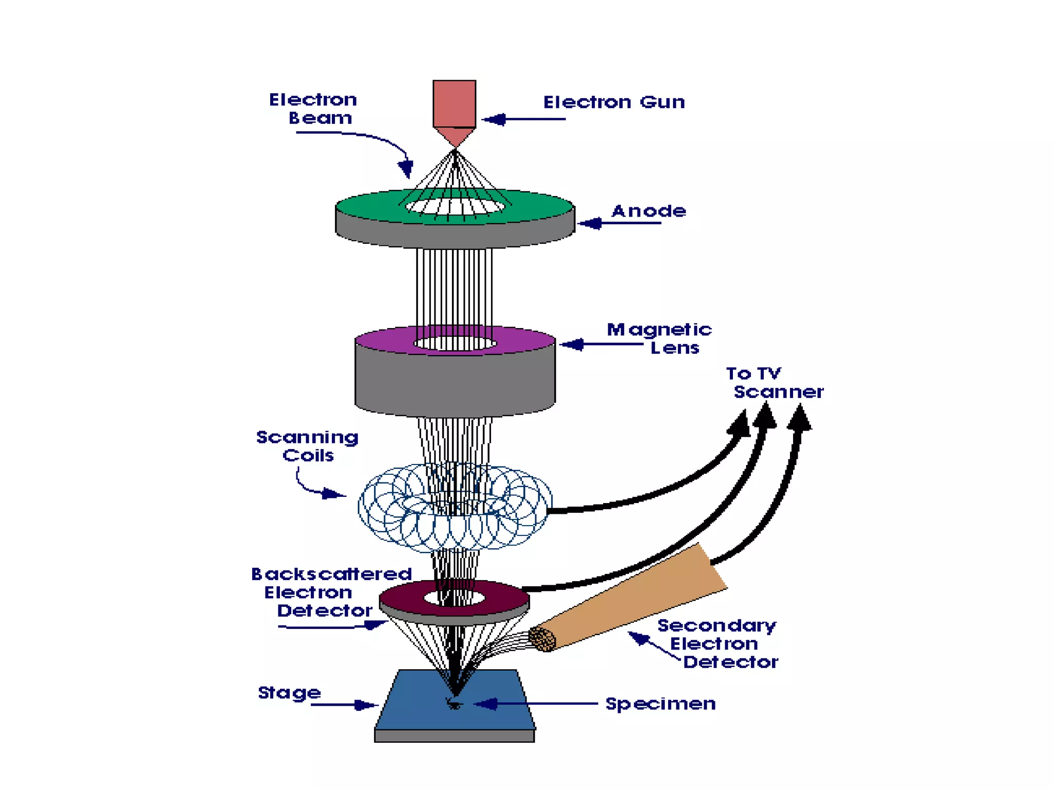
SCANNING ELECTRON Microscopy
Submitted by:-
Manoranjan Purusottam
M.Pharma. 1st sem.
Y19254011
CONTENTS
 Introduction to SEM
 Types of SEM
 Principle
 Instrumentation
 Application
 References
introduction
 A scanning electron microscope is a type of electron
microscope that produces images of a sample by
scanning the surface with a focused beam of
electrons. The electrons interact with atoms in the
sample, producing various signals that contain
information about the sample's surface topography
and composition.
 SEMs can magnify an object from about 10 times up
to 300,000 times. A scale bar is often provided on an
SEM image. From this the actual size of structures in
the image can be calculated.
Types of sem
Conventional (high vacuum) SEM
Variable Pressure or Low Vacuum SEM
Cryo on an SEM (Cryo-SEM)
Environmental SEM
Focused ion beam (FIB)
Electron-beam (E-beam) lithography.
principle
 The signals used by a scanning electron microscope to produce
an image result from interactions of the electron beam with
atoms at various depths within the sample.
 Various types of signals are produced including secondary
electrons (SE), reflected or back-scattered electrons(BSE),
characteristic X-rays and light (cathodoluminescence) (CL),
absorbed current (specimen current) and transmitted electrons .
 In secondary electron imaging, or SEI, the secondary electrons
are emitted from very close to the specimen surface.
 Back-scattered electrons (BSE) are beam electrons that are
reflected from the sample by elastic scattering. They emerge
from deeper locations within the specimen and consequently
the resolution of BSE images is less than SE images.
instrumentation
 The typical scanning electron microscope contains a machine with three components:
1. the microscope column, including the electron gun at the top, the column, down
which the electron beam travels, and the sample chamber at the base.
2. the computer that drives the microscope, with the additional bench controls.
3. ancillary equipment that, for example, analyses composition.
 Electron gun:
Electron guns can be classified into two types-
1. Thermionic gun
2. Field emission gun
 Electron column:
The electron column focuses and illuminates the specimen using the electron beam
generated by the electron gun. As the beam is scanned over the specimen in the X- and
Y- directions, secondary and backscattered electrons are produced and detected. By
amplifying and modulating the brightness of the detected electron signals an image is
produced.
Cont….
 Magnetic lens system:
1. Condenser lens
2. Objective lens
3. Scanning coils
 Detectors:
 Secondary electron detector (SED) – Everhart-Thornley Detector:
Due to the low energies of secondary electrons (SE) (~2 to 50 eV) they are
ejected only from near-surface layers. Therefore, secondary electron
imaging (SEI) is ideal for recording topographical information. To attract
(collect) these low-energy electrons, a small bias (often +/- ve selectable
but usually around +200 to 300V) is applied to the cage at the front end of
the detector to attract the negative electrons towards the detector. A
higher kV (e.g. 7 to 12kV) is applied inside the cage i.e. to the scintillator,
to accelerate the electrons into the scintillator screen.
Cont….
 Backscattered electron detector (BSD) – solid state diode detector:
The BSD is mounted below the objective lens pole piece and
centered around the optic axis. As the specimen surface is scanned
by the incident electron beam, backscattered electrons (BSE) are
generated, the yield of which is controlled by the topographical,
physical and chemical characteristics of the sample. Both
compositional or topographical backscattered electron images (BEI)
can be recorded depending on the window of electron energies
selected for image formation.
 Specimen chamber:
The specimen chamber is maintained at high vacuum that
minimizes scattering of the electron beam before reaching the
specimen. This is important as scattering or attenuation of the
electron beam will increase the probe size and reduce the
resolution, especially in the SE mode. A high vacuum condition also
optimizes collection efficiency.
ADVANTAGES
 Resolution at high magnification.
 Depth of field i.e. the height of a specimen
that appears in focus in an image - more than
300 times the depth of field compared to the
LM.
 Microanalysis i.e. the analysis of sample
composition including information about
chemical composition, as well as
crystallographic, magnetic and electrical
characteristics.
DISADVANTAGES
 SEM cannot take colour images. The colour is often added
artificially in coloured SEM images.
 SEM cannot image through water. An ESEM using a wet
Scanning Transmission Electron Microscope (STEM)
detector can be used to image through thin water films.
 The SEM cannot reliably image charged molecules that are
mobile in a matrix.
 SEM is not good for quantifying surface roughness at small
scale.
 Measurements involving height (z-axis) cannot be taken
directly in an SEM. This requires two images that have been
tilted relative to one another to create a 3D image, and
specialized processing software.
application
 Image compositional and some bonding differences (through
contrast and using backscattered electrons).
 Undertake micro and nano lithography: remove material from
samples; cut pieces out or remove progressive slices from samples
(e.g. using a focused ion beam).
 Heat or cool samples while viewing them (while possible in many
instruments it is generally done only in ESEM or during Cryo-
scanning electron microscopy).
 Wet and dry samples(only in an ESEM).
 View frozen material (in an SEM with a cryostage).
 Generate X-rays from samples for microanalysis.
 Study optoelectronic behavior of semiconductors using
cathodoluminescence.
 View/map grain orientation/crystallographic orientation and study
related information like heterogeneity and micro strain in flat
samples (Electron backscattered diffraction).
REFERENCES
 Stokes, Debbie J. (2008). Principles and Practice
of Variable Pressure Environmental Scanning
Electron Microscopy (VP-ESEM). Chichester: John
Wiley & Sons.
 McMullan, D. (2006). "Scanning electron
microscopy 1928–1965". Scanning. 17 (3): 175–
185.
 McMullan, D. (1988). "Von Ardenne and the
scanning electron microscope". Proc Roy Microsc
Soc. 23: 283–288.
Scanning Electron Microscope (SEM)

Scanning Electron Microscope (SEM)

  • 1.
    SCANNING ELECTRON Microscopy Submittedby:- Manoranjan Purusottam M.Pharma. 1st sem. Y19254011
  • 2.
    CONTENTS  Introduction toSEM  Types of SEM  Principle  Instrumentation  Application  References
  • 3.
    introduction  A scanningelectron microscope is a type of electron microscope that produces images of a sample by scanning the surface with a focused beam of electrons. The electrons interact with atoms in the sample, producing various signals that contain information about the sample's surface topography and composition.  SEMs can magnify an object from about 10 times up to 300,000 times. A scale bar is often provided on an SEM image. From this the actual size of structures in the image can be calculated.
  • 4.
    Types of sem Conventional(high vacuum) SEM Variable Pressure or Low Vacuum SEM Cryo on an SEM (Cryo-SEM) Environmental SEM Focused ion beam (FIB) Electron-beam (E-beam) lithography.
  • 5.
    principle  The signalsused by a scanning electron microscope to produce an image result from interactions of the electron beam with atoms at various depths within the sample.  Various types of signals are produced including secondary electrons (SE), reflected or back-scattered electrons(BSE), characteristic X-rays and light (cathodoluminescence) (CL), absorbed current (specimen current) and transmitted electrons .  In secondary electron imaging, or SEI, the secondary electrons are emitted from very close to the specimen surface.  Back-scattered electrons (BSE) are beam electrons that are reflected from the sample by elastic scattering. They emerge from deeper locations within the specimen and consequently the resolution of BSE images is less than SE images.
  • 8.
    instrumentation  The typicalscanning electron microscope contains a machine with three components: 1. the microscope column, including the electron gun at the top, the column, down which the electron beam travels, and the sample chamber at the base. 2. the computer that drives the microscope, with the additional bench controls. 3. ancillary equipment that, for example, analyses composition.  Electron gun: Electron guns can be classified into two types- 1. Thermionic gun 2. Field emission gun  Electron column: The electron column focuses and illuminates the specimen using the electron beam generated by the electron gun. As the beam is scanned over the specimen in the X- and Y- directions, secondary and backscattered electrons are produced and detected. By amplifying and modulating the brightness of the detected electron signals an image is produced.
  • 9.
    Cont….  Magnetic lenssystem: 1. Condenser lens 2. Objective lens 3. Scanning coils  Detectors:  Secondary electron detector (SED) – Everhart-Thornley Detector: Due to the low energies of secondary electrons (SE) (~2 to 50 eV) they are ejected only from near-surface layers. Therefore, secondary electron imaging (SEI) is ideal for recording topographical information. To attract (collect) these low-energy electrons, a small bias (often +/- ve selectable but usually around +200 to 300V) is applied to the cage at the front end of the detector to attract the negative electrons towards the detector. A higher kV (e.g. 7 to 12kV) is applied inside the cage i.e. to the scintillator, to accelerate the electrons into the scintillator screen.
  • 10.
    Cont….  Backscattered electrondetector (BSD) – solid state diode detector: The BSD is mounted below the objective lens pole piece and centered around the optic axis. As the specimen surface is scanned by the incident electron beam, backscattered electrons (BSE) are generated, the yield of which is controlled by the topographical, physical and chemical characteristics of the sample. Both compositional or topographical backscattered electron images (BEI) can be recorded depending on the window of electron energies selected for image formation.  Specimen chamber: The specimen chamber is maintained at high vacuum that minimizes scattering of the electron beam before reaching the specimen. This is important as scattering or attenuation of the electron beam will increase the probe size and reduce the resolution, especially in the SE mode. A high vacuum condition also optimizes collection efficiency.
  • 11.
    ADVANTAGES  Resolution athigh magnification.  Depth of field i.e. the height of a specimen that appears in focus in an image - more than 300 times the depth of field compared to the LM.  Microanalysis i.e. the analysis of sample composition including information about chemical composition, as well as crystallographic, magnetic and electrical characteristics.
  • 12.
    DISADVANTAGES  SEM cannottake colour images. The colour is often added artificially in coloured SEM images.  SEM cannot image through water. An ESEM using a wet Scanning Transmission Electron Microscope (STEM) detector can be used to image through thin water films.  The SEM cannot reliably image charged molecules that are mobile in a matrix.  SEM is not good for quantifying surface roughness at small scale.  Measurements involving height (z-axis) cannot be taken directly in an SEM. This requires two images that have been tilted relative to one another to create a 3D image, and specialized processing software.
  • 13.
    application  Image compositionaland some bonding differences (through contrast and using backscattered electrons).  Undertake micro and nano lithography: remove material from samples; cut pieces out or remove progressive slices from samples (e.g. using a focused ion beam).  Heat or cool samples while viewing them (while possible in many instruments it is generally done only in ESEM or during Cryo- scanning electron microscopy).  Wet and dry samples(only in an ESEM).  View frozen material (in an SEM with a cryostage).  Generate X-rays from samples for microanalysis.  Study optoelectronic behavior of semiconductors using cathodoluminescence.  View/map grain orientation/crystallographic orientation and study related information like heterogeneity and micro strain in flat samples (Electron backscattered diffraction).
  • 14.
    REFERENCES  Stokes, DebbieJ. (2008). Principles and Practice of Variable Pressure Environmental Scanning Electron Microscopy (VP-ESEM). Chichester: John Wiley & Sons.  McMullan, D. (2006). "Scanning electron microscopy 1928–1965". Scanning. 17 (3): 175– 185.  McMullan, D. (1988). "Von Ardenne and the scanning electron microscope". Proc Roy Microsc Soc. 23: 283–288.