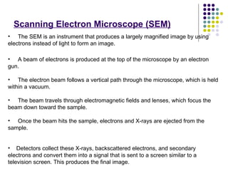
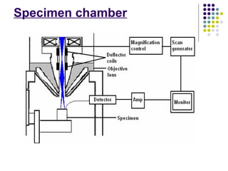
Micro structural Characterization


                                     By
                         Harsha Kamatagi
                       Usn 1ms10mse08
Scanning Electron Microscope (SEM)
• The SEM is an instrument that produces a largely magnified image by using
electrons instead of light to form an image.

• A beam of electrons is produced at the top of the microscope by an electron
gun.

• The electron beam follows a vertical path through the microscope, which is held
within a vacuum.

• The beam travels through electromagnetic fields and lenses, which focus the
beam down toward the sample.

• Once the beam hits the sample, electrons and X-rays are ejected from the
sample.


• Detectors collect these X-rays, backscattered electrons, and secondary
electrons and convert them into a signal that is sent to a screen similar to a
television screen. This produces the final image.
Specimen chamber
Beam-Specimen Interactions
signals
   The beam electron can interact with electric charge field of both
    specimen nucleus and electrons
 These interactions are responsible for a multitude of signal types:
    backscattered electrons, secondary electrons, X-Rays, Auger
    electrons, cathadoluminescence.
 When a beam of electrons interacts with electric charge of a
    specimen atom electron The result is a transfer of energy to the
    specimen atom and a potential expulsion of an electron from that
    atom as a secondary electron (SE).
 If the vacancy due to the creation of a

 secondary electron is filled from a higher
 level orbital, an X-Ray characteristic of that
energy transition is produced.
Hitachi S-4700.
Optical microscope
Comparison between SEM and
optical microscope
optical      sem

Illumination   Light beam   Electron
                            beam
Wave length 2000-7000       .05A
              A
Resolution    Visible       50A
              region on
              2000A
Magnification 10x-20x       10x-2,00,00
                            0x
Depth of       .1microns    30
focus                       mircometer
                            at 1000x
Transmission Electron Microscope (TEM)
Working
   TEMs work the same way except that they shine a beam of electrons (like
    the light) through the specimen(like the slide).

    Whatever part is transmitted is projected onto a phosphor screen for the
    user to see.
   The "Virtual Source" at the top represents the electron gun, producing a
    stream of monochromatic electrons.

   This stream is focused to a small, thin, coherent beam by the use of
    condenser lenses 1 and 2. The first lens largely determines the "spot size";
    the general size range of the final spot that strikes the sample.

   The second lens actually changes the size of the spot on the sample;
    changing it from a wide dispersed spot to a pinpoint beam.
Conti…..
    The beam is restricted by the condenser aperture (usually user selectable),
     knocking out high angle electrons (those far from the optic axis, the dotted
     line down the center)

    The beam strikes the specimen and parts of it are transmitted

    This transmitted portion is focused by the objective lens into an image

    Optional Objective and Selected Area metal apertures can restrict the
     beam; the Objective aperture enhancing contrast by blocking out high-angle
     diffracted electrons

    The image is passed down the column through the intermediate and
     projector lenses, being enlarged all the way
Contd….
   The image strikes the phosphor image screen and light is generated,
    allowing the user to see the image.


    The darker areas of the image represent those areas of the sample that
    fewer electrons were transmitted through (they are thicker or denser).


   The lighter areas of the image represent those areas of the sample that
    more electrons were transmitted through (they are thinner or less dense)
Differences
Auger Electron Spectroscopy

 When an electron beam bombards a solid surface; secondary electrons,
   backscattered electrons, Auger electrons, and characteristic X-rays are
   produced.
Auger Electron Spectroscopy
Auger process

   The basic Auger process starts with the removal of an inner shell
    atomic electron to form a vacancy.
   Several processes are capable of producing the vacancy, but the
    bombardment with an electron beam is the most common one.
   The inner shell vacancy is then filled by a second electron from a
    higher shell. Energy will be simultaneously released.
   A third electron, the Auger electron, is ionized. The excessive
    energy in this process is dissipated as kinetic energy of the Auger
    electron.
   This process of an excited ion decaying into a doubly charged ion
    by the ejection of an electron is called the Auger process.
A typical AES spectrum in the form of d N(E)/dE vs E.

                                   Reference:
                                    J. C. Vickerman, Surface
                                   analysis – the principal
                                   techniques, John Wiley & Sons
Contd…..
   electron spectroscopy is one of the most frequent analytical
    methods for surfaces, thin-films, and interface compositions.


    This wide applicability arises from the combination of surface
    sensitivity (0.5 to 10 nm), good lateral surface resolution (as little as
    10 nm), periodic table coverage (except hydrogen and helium),
References
    FE-SEM Training Manual, Hitachi Scientific Instruments
     http://www.microscopy.ethz.ch/lens.htm
   Joseph Goldstein et al. “Scanning Electron Microscopy
    JEOL 6700 SEM User Manual
    http://www.cas.muohio.edu/~emfweb/EMTheory
    /OH_Index.html
    http://www.gel.usherbrooke.ca/casino/What.html
   http://emalwww.engin.umich.edu/courses/semlectures/semlec.
   anchor659909 David C. Joy. “Low Voltage Scanning Electron
    Microscopy”,
THANK YOU

Sem

  • 1.
    Micro structural Characterization By Harsha Kamatagi Usn 1ms10mse08
  • 2.
    Scanning Electron Microscope(SEM) • The SEM is an instrument that produces a largely magnified image by using electrons instead of light to form an image. • A beam of electrons is produced at the top of the microscope by an electron gun. • The electron beam follows a vertical path through the microscope, which is held within a vacuum. • The beam travels through electromagnetic fields and lenses, which focus the beam down toward the sample. • Once the beam hits the sample, electrons and X-rays are ejected from the sample. • Detectors collect these X-rays, backscattered electrons, and secondary electrons and convert them into a signal that is sent to a screen similar to a television screen. This produces the final image.
  • 5.
  • 6.
  • 7.
    signals  The beam electron can interact with electric charge field of both specimen nucleus and electrons  These interactions are responsible for a multitude of signal types: backscattered electrons, secondary electrons, X-Rays, Auger electrons, cathadoluminescence.  When a beam of electrons interacts with electric charge of a specimen atom electron The result is a transfer of energy to the specimen atom and a potential expulsion of an electron from that atom as a secondary electron (SE).  If the vacancy due to the creation of a secondary electron is filled from a higher level orbital, an X-Ray characteristic of that energy transition is produced.
  • 8.
  • 9.
  • 10.
    Comparison between SEMand optical microscope
  • 11.
    optical sem Illumination Light beam Electron beam Wave length 2000-7000 .05A A Resolution Visible 50A region on 2000A Magnification 10x-20x 10x-2,00,00 0x Depth of .1microns 30 focus mircometer at 1000x
  • 12.
  • 13.
    Working  TEMs work the same way except that they shine a beam of electrons (like the light) through the specimen(like the slide).  Whatever part is transmitted is projected onto a phosphor screen for the user to see.  The "Virtual Source" at the top represents the electron gun, producing a stream of monochromatic electrons.  This stream is focused to a small, thin, coherent beam by the use of condenser lenses 1 and 2. The first lens largely determines the "spot size"; the general size range of the final spot that strikes the sample.  The second lens actually changes the size of the spot on the sample; changing it from a wide dispersed spot to a pinpoint beam.
  • 14.
    Conti…..  The beam is restricted by the condenser aperture (usually user selectable), knocking out high angle electrons (those far from the optic axis, the dotted line down the center)  The beam strikes the specimen and parts of it are transmitted  This transmitted portion is focused by the objective lens into an image  Optional Objective and Selected Area metal apertures can restrict the beam; the Objective aperture enhancing contrast by blocking out high-angle diffracted electrons  The image is passed down the column through the intermediate and projector lenses, being enlarged all the way
  • 15.
    Contd….  The image strikes the phosphor image screen and light is generated, allowing the user to see the image.  The darker areas of the image represent those areas of the sample that fewer electrons were transmitted through (they are thicker or denser).  The lighter areas of the image represent those areas of the sample that more electrons were transmitted through (they are thinner or less dense)
  • 16.
  • 17.
    Auger Electron Spectroscopy When an electron beam bombards a solid surface; secondary electrons, backscattered electrons, Auger electrons, and characteristic X-rays are produced.
  • 18.
  • 19.
    Auger process  The basic Auger process starts with the removal of an inner shell atomic electron to form a vacancy.  Several processes are capable of producing the vacancy, but the bombardment with an electron beam is the most common one.  The inner shell vacancy is then filled by a second electron from a higher shell. Energy will be simultaneously released.  A third electron, the Auger electron, is ionized. The excessive energy in this process is dissipated as kinetic energy of the Auger electron.  This process of an excited ion decaying into a doubly charged ion by the ejection of an electron is called the Auger process.
  • 20.
    A typical AESspectrum in the form of d N(E)/dE vs E. Reference: J. C. Vickerman, Surface analysis – the principal techniques, John Wiley & Sons
  • 21.
    Contd…..  electron spectroscopy is one of the most frequent analytical methods for surfaces, thin-films, and interface compositions.  This wide applicability arises from the combination of surface sensitivity (0.5 to 10 nm), good lateral surface resolution (as little as 10 nm), periodic table coverage (except hydrogen and helium),
  • 22.
    References  FE-SEM Training Manual, Hitachi Scientific Instruments  http://www.microscopy.ethz.ch/lens.htm  Joseph Goldstein et al. “Scanning Electron Microscopy  JEOL 6700 SEM User Manual  http://www.cas.muohio.edu/~emfweb/EMTheory /OH_Index.html  http://www.gel.usherbrooke.ca/casino/What.html  http://emalwww.engin.umich.edu/courses/semlectures/semlec.  anchor659909 David C. Joy. “Low Voltage Scanning Electron Microscopy”,
  • 23.