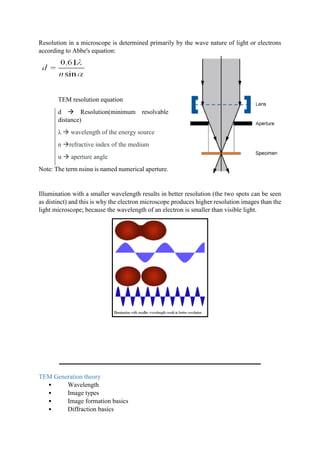
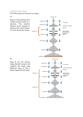
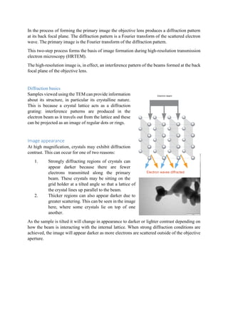
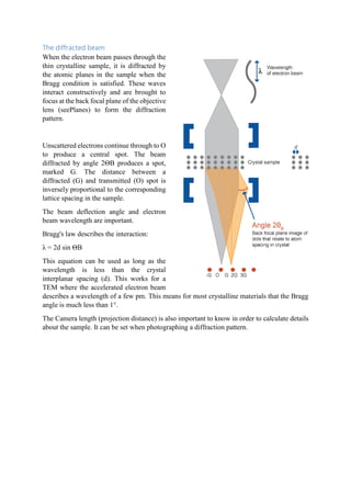
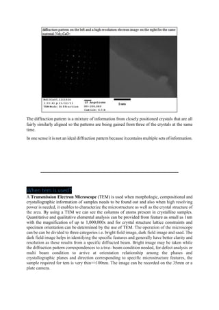
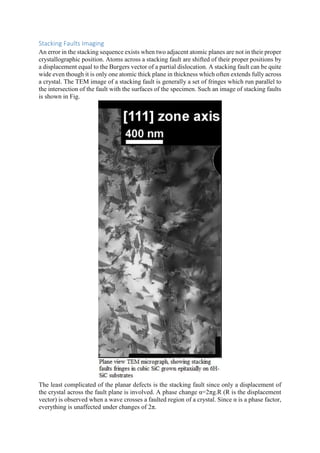
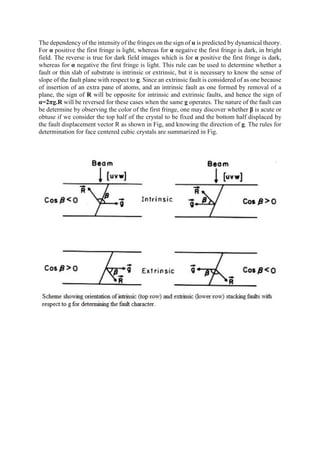
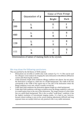
SlideShare a Scribd company logo
1 of 25
Assignment on:
Describe the TEM as a versatile tool for
research in Nanotechnology. How can the
TEM be used to study crystal defects?
Name : Mohit Rajput
Enrolment no. : 12216014
Batch : mt5, tb3
Describe the TEM as a versatile tool for research in
Nanotechnology. How can the TEM be used to study crystal
defects?
As the dimensions of materials developed are reduced, therefore use in the semiconductor
industry of transmission electron microscopes (TEM) have become essential for
characterization. Currently we require high resolution observation and analysis of defects,
materials and structures with nanometer dimensions. The TEM is a popular choice for
nanotechnology as well as semiconductor analysis and production. This type of physical
characterization was traditionally dedicated to advanced characterization due to the destructive
nature of specimen preparation, as well as the fact that it was delicate and time consuming.
More recently, it has been shown that TEM can be performed on specimens and can overcome
past challenges such as cycle time and cost.
What is transmission electron microscopy?
The transmission electron microscope (TEM), the first type of Electron Microscope (EM)
which is an analytical tool allowing visualisation and analysis of specimens in the realms of
microspace (1 micron/1μm = 10-6
m) to nanospace (1 nanometer/nm = 10-9
m). The TEM
reveals levels of detail and complexity inaccessible by light microscopy because it uses a
focused beam of high energy electrons which is allowed by detailed micro-structural
examination through high-resolution and high magnification of specimen through black and
white 2D images which can be seen on a screen or printed onto a photographic plate allowing
for a wide range of educational, science and industry applications. It also enables the
investigation of crystal structures, specimen orientations and chemical compositions of phases,
precipitates and contaminants through diffraction pattern, X-ray and electron-energy analysis.
The word “transmission” means “to pass through”. The way the transmission electron
microscope creates a conventional image which is usually termed a bright field image of a
sample which can be compared to shadow puppetry. Imagine a torch beam shone through a
lattice on a window. The light passes through the transparent parts of the window, but is stopped
by the lattice bars. On a wall beyond, we see the lattice bars as shadows. The TEM uses a beam
of highly energetic electrons instead of light from a torch. On the way through the sample some
parts of the material stop or deflect electrons more than other parts. The electrons are collected
from below the sample onto a phosphorescent screen or through a camera. In the regions where
electrons do not pass through the sample the image is dark. Where electrons are unscattered,
the image is brighter, and there are a range of greys in between depending on the way the
electrons interact with and are scattered by the sample.
Operating Principles of the transmission electron microscope.
Ran to the electron beam collides with an object to be illuminated. By virtue of the power input
to the coil as cathode. When enough energy. Electrons are released. But because of the electron
as it befitted a terminal electron donor. It will run up to the electrodes charged particles in the
air as well. The electron cannot run into the target samples or sample in a microscope, so to
make a vacuum and there will be an increase in light intensity Condenser. Which uses a coil
wrapped around a rod. To induce the direction of the electron beam in the same
direction. Which the intensity of the electron increases.
When a particle or electron beam can be run against an object or workpiece. The beam of light
will be absorbed and the rest can be created through the object to the lens, the Objective Len
the bottom of the lens material and lens system to weed out. The two routes. The image is a
two-dimensional Fluorescence screen screens.
The TEM is a popular choice for nanotechnology as well as semiconductor analysis and
production. They require high voltages to increase the acceleration speed of electrons, which,
once they pass through the sample (transmission), increase the image resolution.
Magnifications of up to 1, 000,000x and resolution below 1 nm are achieved routinely which
can be used to quantitative and qualitative elemental analysis. A scale bar is essential on a TEM
image. From this the actual size of structures in the image can be calculated. For crystalline
phases the crystalline phases the crystal structure, lattice constraints and specimen orientation
can be determined. As we know that electron are negatively charged particles within the atom
therefore electromagnets are used to focus the electron unlike the light which can be focused
by the use of glass lenses.
Concepts related to TEM
The basis fundamental of electron microscopy is the use of an electron beam. It is for this
reason that the TEM requires a vacuum. If air were present the molecules would cause the
beam to scatter. It is also imperative to understand the interactions between the electron beam
and the sample so as to interpret the resulting images. The use of electrons has an impact on
image resolution and absence of colour, and explains the two dimensional nature of
micrographs
Resolution
Definitions
Resolution : It is the ability to distinguish closely spaced points as separate
points.
Resolution Limit : It is the smallest separation of points which can be recognized
as distinct.
Resolving Power : It can be stated as the resolution achieved by a particular
instrument under optimum viewing conditions.
Magnification
Magnification is simply the process of enlarging an image. Once a TEM is calibrated then it is
possible to determine exactly how much enlargement has occurred. This can be recorded on an
image as a scale bar. The use of ‘times magnification’, e.g. 50,000x, will only be accurate for
an image of set/ fixed dimension and so can lead to errors.
Higher magnification will not necessarily give higher resolution. Unless a microscope is
equipped to deliver higher resolution images, higher magnification will only achieve 'empty'
images.
Resolution in a microscope is determined primarily by the wave nature of light or electrons
according to Abbe's equation:
TEM resolution equation
d  Resolution(minimum resolvable
distance)
λ  wavelength of the energy source
n refractive index of the medium
α  aperture angle
Note: The term nsinα is named numerical aperture.
Illumination with a smaller wavelength results in better resolution (the two spots can be seen
as distinct) and this is why the electron microscope produces higher resolution images than the
light microscope; because the wavelength of an electron is smaller than visible light.
TEM Generation theory
• Wavelength
• Image types
• Image formation basics
• Diffraction basics
• Diffraction images
• Combining images
• Imaging mode setup
• Focus/stigmation
The electron wavelength
The wavelength of an electron is dependent upon accelerating voltage and is given by:
Where
h  Plank’s constant (6.626 x 10⁻³⁴
J s)
m  electron mass (9.109 x 10⁻³¹
kg)
e  electronic charge (1.60 x 10⁻¹⁹
C)
V  accelerating voltage (0.5 - 3 x 10⁴
V)
The equation can be approximated to:
The higher the accelerating voltage, the smaller the wavelength of the electrons and the higher
the possible achievable resolution.
Image types
Bright field, HREM and diffraction images
The most common image generated is a bright field image by using a TEM. Some areas of the
sample scatter or absorb electrons and therefore they appear darker. Alternatively other areas
which transmit electrons appear brighter. In simple terms the bright field image appears as a
shadow of the specimen. In the bright field image the objective aperture is used to select the
unscattered electron beam. In doing so, the scattered electrons are excluded from forming the
image. This aperture enhances the contrast in the image.
Dark field images are produced by excluding, using the primary aperture, the primary
(unscattered) beam from the image collected below the sample. The image is produced by
scattered electrons (i.e. only selected electrons are used to form the image). Regions where no
scattering occurs, such as where the primary electron beam passes straight through the sample,
appear black (e.g. in areas around the sample). This kind of imaging is useful in studying crystal
defects, and for the imaging of specific crystallographic phases.
Diffraction images are the result of Bragg scattering as the beam passes through a crystalline
sample. If a “selected area diffraction aperture” is inserted to delimit the region of interest, then
an image created below the sample (in the region called the back focal plane) is seen as an
array of dots (or a set of diffuse rings). This informs the viewer about the crystal structure of
the sample.
Image formation basics
The TEM images are formed in two stages:
A)
Stage A is the scattering of an
incident electron beam by a
specimen. This scattered
radiation passes through an
objective lens, which focuses
it to form the primary image.
B)
Stage B uses the primary
image obtained in stage A and
magnifies this image using
additional lenses to form a
highly magnified final image.
In the process of forming the primary image the objective lens produces a diffraction pattern
at its back focal plane. The diffraction pattern is a Fourier transform of the scattered electron
wave. The primary image is the Fourier transform of the diffraction pattern.
This two-step process forms the basis of image formation during high-resolution transmission
electron microscopy (HRTEM).
The high-resolution image is, in effect, an interference pattern of the beams formed at the back
focal plane of the objective lens.
Diffraction basics
Samples viewed using the TEM can provide information
about its structure, in particular its crystalline nature.
This is because a crystal lattice acts as a diffraction
grating: interference patterns are produced in the
electron beam as it travels out from the lattice and these
can be projected as an image of regular dots or rings.
Image appearance
At high magnification, crystals may exhibit diffraction
contrast. This can occur for one of two reasons:
1. Strongly diffracting regions of crystals can
appear darker because there are fewer
electrons transmitted along the primary
beam. These crystals may be sitting on the
grid holder at a tilted angle so that a lattice of
the crystal lines up parallel to the beam.
2. Thicker regions can also appear darker due to
greater scattering. This can be seen in the image
here, where some crystals lie on top of one
another.
As the sample is tilted it will change in appearance to darker or lighter contrast depending on
how the beam is interacting with the internal lattice. When strong diffraction conditions are
achieved, the image will appear darker as more electrons are scattered outside of the objective
aperture.
The diffracted beam
When the electron beam passes through the
thin crystalline sample, it is diffracted by
the atomic planes in the sample when the
Bragg condition is satisfied. These waves
interact constructively and are brought to
focus at the back focal plane of the objective
lens (seePlanes) to form the diffraction
pattern.
Unscattered electrons continue through to O
to produce a central spot. The beam
diffracted by angle 2ΘB produces a spot,
marked G. The distance between a
diffracted (G) and transmitted (O) spot is
inversely proportional to the corresponding
lattice spacing in the sample.
The beam deflection angle and electron
beam wavelength are important.
Bragg's law describes the interaction:
λ = 2d sin ΘB
This equation can be used as long as the
wavelength is less than the crystal
interplanar spacing (d). This works for a
TEM where the accelerated electron beam
describes a wavelength of a few pm. This means for most crystalline materials that the Bragg
angle is much less than 1°.
The Camera length (projection distance) is also important to know in order to calculate details
about the sample. It can be set when photographing a diffraction pattern.
Tilting
The appearance of a diffraction pattern will depend
on the orientation of the specimen to the electron
beam. If the specimen is tilted so a plane of atoms or
crystallographic direction satisfies the Bragg
condition, distinctive diffraction patterns will be
obtained with diffraction maxima (i.e. spots - often
called reflections) in arrangements which reflect the
crystal structure of the specimen.
To achieve this, samples in a TEM can be tilted.
There are both single-tilt and double-tilt specimen
holders. A double-tilt holder is superior since the
tilting of the sample can be achieved in two axes (X
and Y). It is common to try and tilt a sample so that a
crystal zone axis is, in effect, parallel to the electron beam. Under these conditions a predictable
arrangement of reflections will be present in the diffraction pattern - see the pattern below for
ZnO.
Kikuchi Patterns
Bragg scattering, that is diffraction of inelastically scattered electrons, can lead to the formation
of pairs of parallel lines in the diffraction pattern called Kikuchi lines. For each plane of atoms
in the sample there exists a pair of parallel lines, rather like train lines. The various sets of
Kikuchi lines intersect in diffraction space in a manner which represents the arrangement of
crystal planes in real space. This is called a Kikuchi map. These lines can help an operator to
tilt a crystal around to find different crystal planes. Kikuchi Patterns are a useful phenomenon
to use when initially learning how to tilt crystals because they form regular intersecting lines
over a zone axis.
This spot diffraction pattern shows Kikuchi lines on the left side of the pattern. This pattern is
in the process of being tilted and not yet on the zone axis.
Diffraction patterns
The appearance of the diffraction pattern can reflect the nature of the crystalline phases in the
specimen. For example, if the material is microcrystalline or amorphous the diffraction pattern
consists of a series of concentric rings rather than spots/discs.
Spot patterns
When the electron beam interacts with the sample
when the sample is oriented with a zone axis pattern
parallel to the electron beam, then the diffraction
pattern form in the back focal plane of the objective
lenses a regular array of reflections. This is seen
projected onto the viewing screen as an array of
reflections organized in a predictable manner based
on the crystal structure of the sample.
Convergent Beam Electron Diffraction (CBED)
When the electron beam is converged on the sample to a
point (method = convergent beam), instead of using a parallel
stream of electrons through the sample, the diffraction pattern
forms discs instead of spots in the back focal plane of the
objective lens.
These discs can contain detail that provides information about
the crystal structure of the specimen. In these images we see
almost perfect mirror symmetry in the patterns within the
discs. These symmetries can be used to determine the ponit
and space group of the crystal.
Ring patterns
Sometimes, instead of intensity spots, the electron diffraction
pattern is composed of concentric rings.
Materials that contain no long-range order in the atomic lattice
produce diffuse ring diffraction patterns with no discrete
reflections and one or possibly two diffuse rings of maximum
intensity. Amorphous samples, e.g. polymers and metallic
glasses, produce this kind of pattern.
The bar across the pattern is the “beam stop” used to cover
the bright central beam spot so that the more diffuse rings can
be captured as a digital image.
If the material is a collection of a large number of crystals,
with different orientations, then individual reflections are
seen within the rings
.
Combining images
Images can be combined to get the most information out of a sample.
The diffraction pattern is a mixture of information from closely positioned crystals that are all
fairly similarly aligned so the patterns are being gained from three of the crystals at the same
time.
In one sense it is not an ideal diffraction pattern because it contains multiple sets of information.
When tem is used?
A Transmission Electron Microscope (TEM) is used when morphologic, compositional and
crystallographic information of samples needs to be found out and also when high resolving
power is needed, it enables to characterize the microstructure as well as the crystal structure of
the area. By using a TEM we can see the columns of atoms present in crystalline samples.
Quantitative and qualitative elemental analysis can be provided from feature as small as 1nm
with the magnification of up to 1,000,000x and for crystal structure lattice constraints and
specimen orientation can be determined by the use of TEM. The operation of the microscope
can be can be divided to three categories i.e. bright field image, dark field image and saed. The
dark field image helps in identifying the specific features and generally have better clarity and
resolution as these results from a specific diffracted beam. Bright image may be taken while
the diffraction pattern correspondences to a two- beam condition needed, for defect analysis or
multi beam condition to arrive at orientation relationship among the phases and
crystallographic planes and direction corresponding to specific microstructure features, the
sample required for tem is very thin≈≈100nm. The image can be recorded on the 35mm or a
plate camera.
TEM components
 An electron source (electron gun)
 Thermionic Gun
 Electron beam
 Electromagnetic lenses
 Vacuum chamber
 Chilling system
 Sample/Specimen stage
 Phosphor or fluorescent screen (Image capture)
 Main control panel and operational control
Benefits of using TEM
A Transmission Electron Microscope is an impressive instrument with a number of advantages
such as:
 TEMs offer the most powerful magnification, potentially over one million times or
more
 TEMs have a wide-range of applications and can be utilized in a variety of different
scientific, educational and industrial fields
 TEMs provide information on element and compound structure
 Images are high-quality and detailed
 TEMs are able to yield information of surface features, shape, size and structure
 They are easy to operate with proper training
The transmission electron microscope (TEM) provides the user with advantages over the
microscope in three key areas:
 Resolution at high magnification. Resolution can be defined as the smallest distance
between two closely opposed points, at which they may be recognized as two separate
entities. A typical TEM has a resolution of better than 1 nm.
 Structural information. If the material being viewed has a periodic structure like a
crystal then the beam can interact with that structure in such a way that it diffracts. This
provides information on crystal structure, symmetry and orientation of materials.
 Microanalysis i.e. the analysis of sample chemical composition can be performed in the
TEM.
Application
TEMs have a wide-range of applications in a variety of scientific, education, research and
industrial fields. The Transmission Electron Microscopes has practical applications in such
fields as chemistry, gemology, metallurgy, industry and nanotechnologies as well as provide
information on the topography, morphology, composition and crystallographic data of
samples. TEMs also have many technological and industrial applications, such as
semiconductor inspection, computer chip manufacturing, quality control and can even be used
as part of a production line. The images allow researchers to view samples on a molecular level,
making it possible to analyse structure and texture. Analysis often includes Defect analysis,
failure analysis, materials qualification, electron tomography, structural biology, virology,
forensics, structural composition, chemical composition, steels, aluminium alloys, ceramics
and semiconductor devices. Technology companies use TEMs to identify flaws, fractures and
damages to micro-sized objects; this data can help fix problems and/or help to make a more
durable, efficient product. It also enables the investigation of crystal structures, orientations
and chemical compositions of phases, precipitates and contaminants through diffraction
pattern, characteristic X-ray, and electron energy loss analysis.
Transmission electron microscopy can:
 Image morphology of samples, e.g. view sections of material, fine powders suspended
on a thin film, small whole organisms such as viruses or bacteria, and frozen solutions.
 Tilt a sample and collect a series of images to construct a 3-dimensional image.
 Analyse the composition and some bonding differences (through contrast and by using
spectroscopy techniques: microanalysis and electron energy loss).
 Physically manipulate samples while viewing them, such as indent or compress them
to measure mechanical properties (only when holders specialised for these techniques
are available).
 View frozen material (in a TEM with a cryostage).
 Generate characteristic X-rays from samples for microanalysis.
 Acquire electron diffraction patterns (using the physics of Bragg Diffraction).
 Perform electron energy loss spectroscopy of the beam passing through a sample to
determine sample composition or the bonding states of atoms in the sample.
What is nanotechnology?
The design, characterization, production, and application of structures, devices, and systems
by controlled manipulation of size and shape at the nanometer scale (atomic, molecular, and
macromolecular scale) that produces structures, devices, and systems with at least one
novel/superior characteristic or property.
There are many different views of precisely what is included in nanotechnology. In general,
however, most agree that three things are important:
1. Small size, measured in 100s of nanometers or less
2. Unique properties because of the small size
3. Control the structure and composition on the nm scale in order to control the properties.
Nanostructures—objects with nanometer scale features
So how TEM as a versatile tool for research in Nanotechnology?
As we have come to understand that nanotechnology includes structures having unique
property with small size measured in 100s of nanometer or less therefore for the analysis of
Defect, failure analysis, materials qualification, electron tomography, structural biology,
virology, forensics, structural composition, chemical composition and semiconductor devices
TEM plays an important role. As Transmission Electron Microscope (TEM) is used when
morphologic, compositional and crystallographic information of samples needs to be found out
and also when high resolving power is needed, it enables to characterize the microstructure as
well as the crystal structure of the area. By using a TEM we can see the columns of atoms
present in crystalline samples. Quantitative and qualitative elemental analysis can be provided
from feature as small as 1nm with the magnification of up to 1,000,000x and for crystal
structure lattice constraints and specimen orientation can be determined by the use of TEM.
The operation of the microscope can be can be divided to three categories i.e. bright field
image, dark field image and saed. The dark field image helps in identifying the specific features
and generally have better clarity and resolution as these results from a specific diffracted beam.
Bright image may be taken while the diffraction pattern correspondences to a two- beam
condition needed, for defect analysis or multi beam condition to arrive at orientation
relationship among the phases and crystallographic planes and direction corresponding to
specific microstructure features.
How can a TEM be used to study defect
Transmission electron microscopy (TEM) is till now the most important technique
for studying defects in great detail. Much of what was stated before about defects
would be speculative theory, or would never have been conceived without TEM.
High-Resolution TEM (HRTEM) is the ultimate tool in imaging defects. In favourable cases it
shows directly a two-dimensional projection of the crystal with defects and all.
Some special contrast features arises due to Two-dimensional defects like stacking faults, and
also by grain- and phase boundaries to some extent. Stacking faults are best seen and identified
under dynamical two-beam condition; i.e. the Bragg condition is exactly met for one point in
the reciprocal lattice. This implies that if the diffracted beam is seen as the primary beam, also
meets the Bragg condition; it is diffracted back into the primary beam wave field. This leads to
an oscillation of the intensity between the primary and the diffracted beam as a function of
depth in the sample; the "wave length" of this periodic intensity variations is called the
extinction length ξ.
Technology companies use TEMs to identify flaws, fractures and damages to micro-sized
objects; this data can help fix problems and/or help to make a more durable, efficient product.
TEM image simulations
Every image detail, or contrast, appearing on the phosphorescent screen of a transmission
electron microscope (TEM) is the result of the interaction of the electron beam with the sample.
Unlike the direct interpretation we can give of the eye visible world, the interpretation of TEM
micrographs is far from straightforward and has to be considered carefully. The origins of the
TEM contrasts are complex and multiple. They are divided here into the following four
categories:
1. Absorption contrast,
2. Structure contrast,
3. Diffraction contrast,
4. Phase contrast.
The contrast formation theories, even though based on sometimes tricky approximations, give
a good description of the TEM images. With the help of these theories, the TEM images can
be reproduced by large numerical calculations. The image simulation appears as a powerful
tool for the identification of an object at the origin of an observed contrast.
Samples can exhibit diffraction contrast, whereby the electron beam undergoes Bragg
scattering, which in the case of a crystalline sample, disperses electrons into discrete locations
in the back focal plane. By the placement of apertures in the back focal plane, i.e. the objective
aperture, the desired Bragg reflections can be selected (or excluded), thus only parts of the
sample that are causing the electrons to scatter to the selected reflections will end up projected
onto the imaging apparatus. Applications for this method include the identification of lattice
defects in crystals.
Crystal structure can also be investigated by high-resolution transmission electron microscopy
(HRTEM), also known as phase contrast. When utilizing a Field emission source and a
specimen of uniform thickness, the images are formed due to differences in phase of electron
waves, which is caused by specimen interaction
Contrast in Imperfect Crystals – Defect Imaging
For getting best diffraction contrast from defects it is advisory for the specimen to be tilted so
that we have two-beam condition with slight deviation from the Bragg conditions. This is
measured by the vector s (K=g+s, where K is diffraction vector and g is reciprocal lattice
vector), which is called the excitation error or deviation parameter.
If the excess Kikuchi line lies outside its corresponding diffraction spot g, we say that s>0.
Alternatively if the excess Kikuchi line lies inside it corresponding diffraction spot g we say
that s<0 and we say that s=0 when the Kikuchi line runs through its corresponding spot g
exactly as it can be seen from Fig. The best possible strong-beam image contrast conditions is
small and positive deviation parameter s for a defect imaging.
Dislocation Imaging
For understanding why contrast from dislocation is observed, one should understand the
schematic diagram in Fig. If the diffraction geometry is set slightly away from the Bragg
conditions, the distortion due to the dislocation will then bend the near-diffracting planes back
into the Bragg-diffracting conditions. So, regions either sides of the dislocation core are at the
Bragg condition for ±ghkl, while the regions far from the dislocation are tilted well away from
the Bragg condition.
Important information which needs to be extracted from TEM images regarding dislocations
are:
1) The direction and the magnitude of the Burgers vector, b, which is normal to the hkl
diffracting planes;
2) The direction of line (a vector) and also the character of the dislocation (edge, screw,
or mixed);
3) The glide plane;
4) The density of the dislocations;
5) If the dislocations are interacting with other each another or other defects.
A general rule that can be used to determine the Burgers vector is the called “g.b rule”, which
states that if the Burgers vector of the dislocation is perpendicular to the active diffraction
vector, i.e. g.b=0, there is absence of diffraction contrast from the dislocation. The dislocation
is invisible. This is well illustrated by Fig.
Stacking Faults Imaging
An error in the stacking sequence exists when two adjacent atomic planes are not in their proper
crystallographic position. Atoms across a stacking fault are shifted of their proper positions by
a displacement equal to the Burgers vector of a partial dislocation. A stacking fault can be quite
wide even though it is only one atomic thick plane in thickness which often extends fully across
a crystal. The TEM image of a stacking fault is generally a set of fringes which run parallel to
the intersection of the fault with the surfaces of the specimen. Such an image of stacking faults
is shown in Fig.
The least complicated of the planar defects is the stacking fault since only a displacement of
the crystal across the fault plane is involved. A phase change α=2πg.R (R is the displacement
vector) is observed when a wave crosses a faulted region of a crystal. Since α is a phase factor,
everything is unaffected under changes of 2π.
The dependency of the intensity of the fringes on the sign of α is predicted by dynamical theory.
For α positive the first fringe is light, whereas for α negative the first fringe is dark, in bright
field. The reverse is true for dark field images which is for α positive the first fringe is dark,
whereas for α negative the first fringe is light. This rule can be used to determine whether a
fault or thin slab of substrate is intrinsic or extrinsic, but it is necessary to know the sense of
slope of the fault plane with respect to g. Since an extrinsic fault is considered of as one because
of insertion of an extra pane of atoms, and an intrinsic fault as one formed by removal of a
plane, the sign of R will be opposite for intrinsic and extrinsic faults, and hence the sign of
α=2πg.R will be reversed for these cases when the same g operates. The nature of the fault can
be determine by observing the color of the first fringe, one may discover whether β is acute or
obtuse if we consider the top half of the crystal to be fixed and the bottom half displaced by
the fault displacement vector R as shown in Fig, and knowing the direction of g. The rules for
determination for face centered cubic crystals are summarized in Fig.
We may draw the following conclusions
They are justified by the full theory of TEM contrast.
• Dislocations are invisible or exhibit only weak contrast if g • b = 0. This can be used
for a Burgers vector analysis by imaging the same dislocation with different diffraction
vectors and observing the contrast.
• Under kinematic bright field conditions (Bragg condition met almost, but not quite),
the dislocation is imaged as a dark line on a bright background. The width of the line
corresponds to the width of the region next to one side of the dislocation where the
Bragg condition is now met; which is usually several nm.
• Under dark field conditions the dislocation appears bright on a dark background.
• Under dark field conditions with large excitation errors the Bragg condition is only met
in a small region close to the core of the dislocation. The image consists of a thin white
line on a pitch black background. This is the so-called "weak-beam" condition; it has
the highest resolution of conventional imaging modes. It is hard to use, however,
because almost nothing is seen on the screen (making adjustments difficult) and long
exposure times are needed which are only practical with a very stable instrument.
References
1. Abramowitz M, Davidson MW (2007). "Introduction to Microscopy". Molecular
Expressions. Retrieved 2007-08-22.
2. Abramowitz M, Davidson MW (2003-08-01). "Darkfield Illumination". Retrieved
2008-10-21.
3. Fultz, B and Howe, J (2007). Transmission Electron Microscopy and Diffractometry
of Materials. Springer. ISBN 3-540-73885-1.
4. Champness, P. E. (2001). Electron Diffraction in the Transmission Electron
Microscope. Garland Science. ISBN 1-85996-147-9. ISSN 978-1859961476.
5. Hubbard, A (1995). The Handbook of surface imaging and visualization. CRC Press.
ISBN 0-8493-8911-9.
6. Williams, D and Carter, C. B. (1996). Transmission Electron Microscopy. 1 – Basics.
Plenum Press. ISBN 0-306-45324-X.
7. Cowley, J. M (1995). Diffraction physics. Elsevier Science B. V. ISBN 0-444-82218-
6.
8. Michael A. O’Keefe and Lawrence F. Allard. "Sub-Ångstrom Electron Microscopy
for Sub-Ångstrom Nano-Metrology". National Nanotechnology Initiative Workshop
on Instrumentation and Metrology for Nanotechnology, Gaithersburg, MD (2004).
9. Transmission Electron Microscopy, D.B.Williams and C.B.Carter, Plenum Press,
New York, 1996.
10. Transmission Electron Microscopy and Diffractometry of Materials, B.Fultz and J.M.
Howe, Springer-Verlag Berlin Heidelberg New York 2001.
11. Transmission Electron Microscopy and Diffractometry of Materials, B.Fultz and J.M.
Howe, Springer-Verlag Berlin Heidelberg New York 2001.
12. Electron Beam Analysis of Materials, M.H. Loretto, Chapman and Hall, London New
York 1984.
13. http://www-hrem.msm.cam.ac.uk/research/EFTEM/EFTEM.html
14. http://www.microscopy.ethz.ch/
15. www.matter.org.uk
16. Wikipedia
17. Science direct
18. Clustered data collected from Internet and banner at lab.

More Related Content

What's hot

Transmission electron microscope
Transmission electron microscopeTransmission electron microscope
Transmission electron microscopesoniaangeline
 
Modern Techniques of Materials Characterisation
Modern Techniques of Materials CharacterisationModern Techniques of Materials Characterisation
Modern Techniques of Materials CharacterisationDr. Ramesh B
 
Transmission Electron Microscope
Transmission Electron MicroscopeTransmission Electron Microscope
Transmission Electron Microscope20was
 
Transmission Electron Microscopy (TEM)
Transmission Electron Microscopy (TEM) Transmission Electron Microscopy (TEM)
Transmission Electron Microscopy (TEM) Zohaib HUSSAIN
 
Transmission Electron Microscopy
Transmission Electron MicroscopyTransmission Electron Microscopy
Transmission Electron MicroscopySejal9787
 
Examples of Various Imaging Techniques- SEM, AFM, TEM and Fluorescence
Examples of Various Imaging Techniques- SEM, AFM, TEM and FluorescenceExamples of Various Imaging Techniques- SEM, AFM, TEM and Fluorescence
Examples of Various Imaging Techniques- SEM, AFM, TEM and FluorescenceJacob Feste
 
ELECTRON MICROSCOPY (TEM & SEM)
ELECTRON MICROSCOPY (TEM & SEM)ELECTRON MICROSCOPY (TEM & SEM)
ELECTRON MICROSCOPY (TEM & SEM)ADITYA ARYA
 
Transmission electron microscope
Transmission electron microscopeTransmission electron microscope
Transmission electron microscopeMonika Uma Shankar
 
Electron microscope
Electron microscopeElectron microscope
Electron microscopeASRAF SOHEL
 
Transmission electron microscope
Transmission electron microscopeTransmission electron microscope
Transmission electron microscopeRaj Mohan
 
Electron microscopy to study the micro organisms
Electron microscopy to study the micro organismsElectron microscopy to study the micro organisms
Electron microscopy to study the micro organismsNoushinAfshan
 
TRANSMISSION ELECTRON MICROSCOPY
TRANSMISSION ELECTRON MICROSCOPYTRANSMISSION ELECTRON MICROSCOPY
TRANSMISSION ELECTRON MICROSCOPYSutapa Saha
 
Scanning and transmission electron microscopy
Scanning and transmission electron microscopyScanning and transmission electron microscopy
Scanning and transmission electron microscopygohil sanjay bhagvanji
 

What's hot (20)

Tem 1
Tem  1Tem  1
Tem 1
 
Dip mukhtiar
Dip mukhtiarDip mukhtiar
Dip mukhtiar
 
Transmission electron microscope
Transmission electron microscopeTransmission electron microscope
Transmission electron microscope
 
Modern Techniques of Materials Characterisation
Modern Techniques of Materials CharacterisationModern Techniques of Materials Characterisation
Modern Techniques of Materials Characterisation
 
Transmission Electron Microscope
Transmission Electron MicroscopeTransmission Electron Microscope
Transmission Electron Microscope
 
Transmission Electron Microscopy (TEM)
Transmission Electron Microscopy (TEM) Transmission Electron Microscopy (TEM)
Transmission Electron Microscopy (TEM)
 
Transmission Electron Microscopy
Transmission Electron MicroscopyTransmission Electron Microscopy
Transmission Electron Microscopy
 
Tem ppt
Tem ppt Tem ppt
Tem ppt
 
Examples of Various Imaging Techniques- SEM, AFM, TEM and Fluorescence
Examples of Various Imaging Techniques- SEM, AFM, TEM and FluorescenceExamples of Various Imaging Techniques- SEM, AFM, TEM and Fluorescence
Examples of Various Imaging Techniques- SEM, AFM, TEM and Fluorescence
 
ELECTRON MICROSCOPY (TEM & SEM)
ELECTRON MICROSCOPY (TEM & SEM)ELECTRON MICROSCOPY (TEM & SEM)
ELECTRON MICROSCOPY (TEM & SEM)
 
Transmission electron microscope
Transmission electron microscopeTransmission electron microscope
Transmission electron microscope
 
Electron microscopy
Electron microscopyElectron microscopy
Electron microscopy
 
Transmission electron
Transmission        electronTransmission        electron
Transmission electron
 
Electron microscope
Electron microscopeElectron microscope
Electron microscope
 
Electron microscope
Electron microscopeElectron microscope
Electron microscope
 
Transmission electron microscope
Transmission electron microscopeTransmission electron microscope
Transmission electron microscope
 
Electron Microscopy
Electron MicroscopyElectron Microscopy
Electron Microscopy
 
Electron microscopy to study the micro organisms
Electron microscopy to study the micro organismsElectron microscopy to study the micro organisms
Electron microscopy to study the micro organisms
 
TRANSMISSION ELECTRON MICROSCOPY
TRANSMISSION ELECTRON MICROSCOPYTRANSMISSION ELECTRON MICROSCOPY
TRANSMISSION ELECTRON MICROSCOPY
 
Scanning and transmission electron microscopy
Scanning and transmission electron microscopyScanning and transmission electron microscopy
Scanning and transmission electron microscopy
 

Viewers also liked

Aula 006 - Filtros
Aula 006 - FiltrosAula 006 - Filtros
Aula 006 - FiltrosOsmar Rios
 
Diferenças entre maquinas digitais e analógicas
Diferenças entre maquinas digitais e analógicasDiferenças entre maquinas digitais e analógicas
Diferenças entre maquinas digitais e analógicasDiiGomes
 
Equipamentos de captura câmaras fotográficas digitais
Equipamentos de captura câmaras fotográficas digitaisEquipamentos de captura câmaras fotográficas digitais
Equipamentos de captura câmaras fotográficas digitaisGonçalo Soares
 
Tudo sobre a reflex NIKON
Tudo sobre a reflex NIKONTudo sobre a reflex NIKON
Tudo sobre a reflex NIKONSuperSGaming
 
Máquina ou câmera fotográfica digital e analógica
Máquina ou câmera fotográfica digital e analógicaMáquina ou câmera fotográfica digital e analógica
Máquina ou câmera fotográfica digital e analógicabloblogcom
 
Aula 005 - Fotografia digital e equipamentos
Aula 005 - Fotografia digital e equipamentosAula 005 - Fotografia digital e equipamentos
Aula 005 - Fotografia digital e equipamentosOsmar Rios
 
Tipos de câmeras fotográficas
Tipos de câmeras fotográficasTipos de câmeras fotográficas
Tipos de câmeras fotográficasDanieltf12
 
O Projeto Audiovisual 2[1]
O Projeto Audiovisual 2[1]O Projeto Audiovisual 2[1]
O Projeto Audiovisual 2[1]videoparatodos
 

Viewers also liked (8)

Aula 006 - Filtros
Aula 006 - FiltrosAula 006 - Filtros
Aula 006 - Filtros
 
Diferenças entre maquinas digitais e analógicas
Diferenças entre maquinas digitais e analógicasDiferenças entre maquinas digitais e analógicas
Diferenças entre maquinas digitais e analógicas
 
Equipamentos de captura câmaras fotográficas digitais
Equipamentos de captura câmaras fotográficas digitaisEquipamentos de captura câmaras fotográficas digitais
Equipamentos de captura câmaras fotográficas digitais
 
Tudo sobre a reflex NIKON
Tudo sobre a reflex NIKONTudo sobre a reflex NIKON
Tudo sobre a reflex NIKON
 
Máquina ou câmera fotográfica digital e analógica
Máquina ou câmera fotográfica digital e analógicaMáquina ou câmera fotográfica digital e analógica
Máquina ou câmera fotográfica digital e analógica
 
Aula 005 - Fotografia digital e equipamentos
Aula 005 - Fotografia digital e equipamentosAula 005 - Fotografia digital e equipamentos
Aula 005 - Fotografia digital e equipamentos
 
Tipos de câmeras fotográficas
Tipos de câmeras fotográficasTipos de câmeras fotográficas
Tipos de câmeras fotográficas
 
O Projeto Audiovisual 2[1]
O Projeto Audiovisual 2[1]O Projeto Audiovisual 2[1]
O Projeto Audiovisual 2[1]
 

Similar to TEM versatile tool (small version)

Transmission electron microscope (TEM) Likhith K
Transmission electron microscope  (TEM) Likhith KTransmission electron microscope  (TEM) Likhith K
Transmission electron microscope (TEM) Likhith KLIKHITHK1
 
Transmission electron microscope, high resolution tem and selected area elect...
Transmission electron microscope, high resolution tem and selected area elect...Transmission electron microscope, high resolution tem and selected area elect...
Transmission electron microscope, high resolution tem and selected area elect...Nano Encryption
 
Principle & Applications of Transmission Electron Microscopy (TEM) & High Res...
Principle & Applications of Transmission Electron Microscopy (TEM) & High Res...Principle & Applications of Transmission Electron Microscopy (TEM) & High Res...
Principle & Applications of Transmission Electron Microscopy (TEM) & High Res...Gulfam Raza
 
2018 HM-scanning electron microscope
2018 HM-scanning electron microscope2018 HM-scanning electron microscope
2018 HM-scanning electron microscopeHarsh Mohan
 
Electron microscope
Electron microscopeElectron microscope
Electron microscopejakkaas
 
ELECTRON MICROSCOPY-Scanning Electron MicroscopySEM.pptx
ELECTRON MICROSCOPY-Scanning Electron MicroscopySEM.pptxELECTRON MICROSCOPY-Scanning Electron MicroscopySEM.pptx
ELECTRON MICROSCOPY-Scanning Electron MicroscopySEM.pptxSagarBhakare1
 
Scanning and transmission electroscopy.pptx
Scanning and transmission electroscopy.pptxScanning and transmission electroscopy.pptx
Scanning and transmission electroscopy.pptxNirmal P J
 
Materials Characterization
Materials CharacterizationMaterials Characterization
Materials CharacterizationVikas Barnwal
 
10. The Transmission Electron Microscope (TEM).pptx
10. The Transmission Electron Microscope (TEM).pptx10. The Transmission Electron Microscope (TEM).pptx
10. The Transmission Electron Microscope (TEM).pptxRENERGISTICS
 
Advanced Characterization Technique - SEM
Advanced Characterization Technique - SEMAdvanced Characterization Technique - SEM
Advanced Characterization Technique - SEMIlyas Hussain
 
Types of electron microscope
Types of electron microscopeTypes of electron microscope
Types of electron microscopeAsad Leo
 
Tunneling electron Microscopy, Scanning electron microscopy
Tunneling electron Microscopy, Scanning electron microscopyTunneling electron Microscopy, Scanning electron microscopy
Tunneling electron Microscopy, Scanning electron microscopyelminehtsegahun2
 

Similar to TEM versatile tool (small version) (20)

Transmission electron microscope (TEM) Likhith K
Transmission electron microscope  (TEM) Likhith KTransmission electron microscope  (TEM) Likhith K
Transmission electron microscope (TEM) Likhith K
 
Transmission electron microscope, high resolution tem and selected area elect...
Transmission electron microscope, high resolution tem and selected area elect...Transmission electron microscope, high resolution tem and selected area elect...
Transmission electron microscope, high resolution tem and selected area elect...
 
Principle & Applications of Transmission Electron Microscopy (TEM) & High Res...
Principle & Applications of Transmission Electron Microscopy (TEM) & High Res...Principle & Applications of Transmission Electron Microscopy (TEM) & High Res...
Principle & Applications of Transmission Electron Microscopy (TEM) & High Res...
 
Transmission Electron Microscopy
Transmission Electron MicroscopyTransmission Electron Microscopy
Transmission Electron Microscopy
 
Tem
TemTem
Tem
 
2018 HM-scanning electron microscope
2018 HM-scanning electron microscope2018 HM-scanning electron microscope
2018 HM-scanning electron microscope
 
Electron microscope
Electron microscopeElectron microscope
Electron microscope
 
SEM,TEM & AFM
SEM,TEM & AFMSEM,TEM & AFM
SEM,TEM & AFM
 
ELECTRON MICROSCOPY-Scanning Electron MicroscopySEM.pptx
ELECTRON MICROSCOPY-Scanning Electron MicroscopySEM.pptxELECTRON MICROSCOPY-Scanning Electron MicroscopySEM.pptx
ELECTRON MICROSCOPY-Scanning Electron MicroscopySEM.pptx
 
SEM and TEM
SEM and  TEMSEM and  TEM
SEM and TEM
 
Scanning and transmission electroscopy.pptx
Scanning and transmission electroscopy.pptxScanning and transmission electroscopy.pptx
Scanning and transmission electroscopy.pptx
 
Sem Poster
Sem PosterSem Poster
Sem Poster
 
Microscope
MicroscopeMicroscope
Microscope
 
Sem
SemSem
Sem
 
Materials Characterization
Materials CharacterizationMaterials Characterization
Materials Characterization
 
10. The Transmission Electron Microscope (TEM).pptx
10. The Transmission Electron Microscope (TEM).pptx10. The Transmission Electron Microscope (TEM).pptx
10. The Transmission Electron Microscope (TEM).pptx
 
Advanced Characterization Technique - SEM
Advanced Characterization Technique - SEMAdvanced Characterization Technique - SEM
Advanced Characterization Technique - SEM
 
Types of electron microscope
Types of electron microscopeTypes of electron microscope
Types of electron microscope
 
Scanning electron microscopy
Scanning electron microscopyScanning electron microscopy
Scanning electron microscopy
 
Tunneling electron Microscopy, Scanning electron microscopy
Tunneling electron Microscopy, Scanning electron microscopyTunneling electron Microscopy, Scanning electron microscopy
Tunneling electron Microscopy, Scanning electron microscopy
 

More from Mohit Rajput

Understanding Association Rule Mining
Understanding Association Rule MiningUnderstanding Association Rule Mining
Understanding Association Rule MiningMohit Rajput
 
Understanding known _ unknown - known _ unknown
Understanding known _ unknown - known _ unknownUnderstanding known _ unknown - known _ unknown
Understanding known _ unknown - known _ unknownMohit Rajput
 
Algorithms in Reinforcement Learning
Algorithms in Reinforcement LearningAlgorithms in Reinforcement Learning
Algorithms in Reinforcement LearningMohit Rajput
 
Understanding Bagging and Boosting
Understanding Bagging and BoostingUnderstanding Bagging and Boosting
Understanding Bagging and BoostingMohit Rajput
 
Dissertation mid evaluation
Dissertation mid evaluationDissertation mid evaluation
Dissertation mid evaluationMohit Rajput
 
For Seminar - Prospect: Development of continuous CNT path in BCP using sel...
For Seminar - Prospect:  Development of continuous CNT path in BCP using  sel...For Seminar - Prospect:  Development of continuous CNT path in BCP using  sel...
For Seminar - Prospect: Development of continuous CNT path in BCP using sel...Mohit Rajput
 
Mid-Dissertation Work Done Report
Mid-Dissertation Work Done ReportMid-Dissertation Work Done Report
Mid-Dissertation Work Done ReportMohit Rajput
 
Mid-Dissertation Work Report Presentation
Mid-Dissertation Work Report Presentation  Mid-Dissertation Work Report Presentation
Mid-Dissertation Work Report Presentation Mohit Rajput
 
SURA Final report PVDF-CNT
SURA Final report PVDF-CNTSURA Final report PVDF-CNT
SURA Final report PVDF-CNTMohit Rajput
 
R markup code to create Regression Model
R markup code to create Regression ModelR markup code to create Regression Model
R markup code to create Regression ModelMohit Rajput
 
Regression Model for movies
Regression Model for moviesRegression Model for movies
Regression Model for moviesMohit Rajput
 
Presentation- BCP self assembly meshes
Presentation- BCP self assembly meshesPresentation- BCP self assembly meshes
Presentation- BCP self assembly meshesMohit Rajput
 
Presentation- Multilayer block copolymer meshes by orthogonal self-assembly
Presentation- Multilayer block copolymer  meshes by orthogonal self-assemblyPresentation- Multilayer block copolymer  meshes by orthogonal self-assembly
Presentation- Multilayer block copolymer meshes by orthogonal self-assemblyMohit Rajput
 
Cover for report on Biofuels Generation
Cover for report on Biofuels GenerationCover for report on Biofuels Generation
Cover for report on Biofuels GenerationMohit Rajput
 
A Report on Metal Drawing Operations
A Report on Metal Drawing OperationsA Report on Metal Drawing Operations
A Report on Metal Drawing OperationsMohit Rajput
 
A technical report on BioFuels Generation
A technical report on BioFuels GenerationA technical report on BioFuels Generation
A technical report on BioFuels GenerationMohit Rajput
 
Presentation - Bio-fuels Generation
Presentation - Bio-fuels GenerationPresentation - Bio-fuels Generation
Presentation - Bio-fuels GenerationMohit Rajput
 
Status of Education in India by Mohit Rajput
Status of Education in India by Mohit RajputStatus of Education in India by Mohit Rajput
Status of Education in India by Mohit RajputMohit Rajput
 
Internship Presentation on Characterization of Stainless Steel-Titanium Diffu...
Internship Presentation on Characterization of Stainless Steel-Titanium Diffu...Internship Presentation on Characterization of Stainless Steel-Titanium Diffu...
Internship Presentation on Characterization of Stainless Steel-Titanium Diffu...Mohit Rajput
 

More from Mohit Rajput (20)

Understanding Association Rule Mining
Understanding Association Rule MiningUnderstanding Association Rule Mining
Understanding Association Rule Mining
 
Understanding known _ unknown - known _ unknown
Understanding known _ unknown - known _ unknownUnderstanding known _ unknown - known _ unknown
Understanding known _ unknown - known _ unknown
 
Algorithms in Reinforcement Learning
Algorithms in Reinforcement LearningAlgorithms in Reinforcement Learning
Algorithms in Reinforcement Learning
 
Understanding Bagging and Boosting
Understanding Bagging and BoostingUnderstanding Bagging and Boosting
Understanding Bagging and Boosting
 
Dissertation mid evaluation
Dissertation mid evaluationDissertation mid evaluation
Dissertation mid evaluation
 
For Seminar - Prospect: Development of continuous CNT path in BCP using sel...
For Seminar - Prospect:  Development of continuous CNT path in BCP using  sel...For Seminar - Prospect:  Development of continuous CNT path in BCP using  sel...
For Seminar - Prospect: Development of continuous CNT path in BCP using sel...
 
Mid-Dissertation Work Done Report
Mid-Dissertation Work Done ReportMid-Dissertation Work Done Report
Mid-Dissertation Work Done Report
 
Mid-Dissertation Work Report Presentation
Mid-Dissertation Work Report Presentation  Mid-Dissertation Work Report Presentation
Mid-Dissertation Work Report Presentation
 
Sura ppt final
Sura ppt finalSura ppt final
Sura ppt final
 
SURA Final report PVDF-CNT
SURA Final report PVDF-CNTSURA Final report PVDF-CNT
SURA Final report PVDF-CNT
 
R markup code to create Regression Model
R markup code to create Regression ModelR markup code to create Regression Model
R markup code to create Regression Model
 
Regression Model for movies
Regression Model for moviesRegression Model for movies
Regression Model for movies
 
Presentation- BCP self assembly meshes
Presentation- BCP self assembly meshesPresentation- BCP self assembly meshes
Presentation- BCP self assembly meshes
 
Presentation- Multilayer block copolymer meshes by orthogonal self-assembly
Presentation- Multilayer block copolymer  meshes by orthogonal self-assemblyPresentation- Multilayer block copolymer  meshes by orthogonal self-assembly
Presentation- Multilayer block copolymer meshes by orthogonal self-assembly
 
Cover for report on Biofuels Generation
Cover for report on Biofuels GenerationCover for report on Biofuels Generation
Cover for report on Biofuels Generation
 
A Report on Metal Drawing Operations
A Report on Metal Drawing OperationsA Report on Metal Drawing Operations
A Report on Metal Drawing Operations
 
A technical report on BioFuels Generation
A technical report on BioFuels GenerationA technical report on BioFuels Generation
A technical report on BioFuels Generation
 
Presentation - Bio-fuels Generation
Presentation - Bio-fuels GenerationPresentation - Bio-fuels Generation
Presentation - Bio-fuels Generation
 
Status of Education in India by Mohit Rajput
Status of Education in India by Mohit RajputStatus of Education in India by Mohit Rajput
Status of Education in India by Mohit Rajput
 
Internship Presentation on Characterization of Stainless Steel-Titanium Diffu...
Internship Presentation on Characterization of Stainless Steel-Titanium Diffu...Internship Presentation on Characterization of Stainless Steel-Titanium Diffu...
Internship Presentation on Characterization of Stainless Steel-Titanium Diffu...
 

Recently uploaded

Swan(sea) Song – personal research during my six years at Swansea ... and bey...
Swan(sea) Song – personal research during my six years at Swansea ... and bey...Swan(sea) Song – personal research during my six years at Swansea ... and bey...
Swan(sea) Song – personal research during my six years at Swansea ... and bey...Alan Dix
 
Hyderabad Call Girls Khairatabad ✨ 7001305949 ✨ Cheap Price Your Budget
Hyderabad Call Girls Khairatabad ✨ 7001305949 ✨ Cheap Price Your BudgetHyderabad Call Girls Khairatabad ✨ 7001305949 ✨ Cheap Price Your Budget
Hyderabad Call Girls Khairatabad ✨ 7001305949 ✨ Cheap Price Your BudgetEnjoy Anytime
 
SQL Database Design For Developers at php[tek] 2024
SQL Database Design For Developers at php[tek] 2024SQL Database Design For Developers at php[tek] 2024
SQL Database Design For Developers at php[tek] 2024Scott Keck-Warren
 
08448380779 Call Girls In Civil Lines Women Seeking Men
08448380779 Call Girls In Civil Lines Women Seeking Men08448380779 Call Girls In Civil Lines Women Seeking Men
08448380779 Call Girls In Civil Lines Women Seeking MenDelhi Call girls
 
Install Stable Diffusion in windows machine
Install Stable Diffusion in windows machineInstall Stable Diffusion in windows machine
Install Stable Diffusion in windows machinePadma Pradeep
 
Enhancing Worker Digital Experience: A Hands-on Workshop for Partners
Enhancing Worker Digital Experience: A Hands-on Workshop for PartnersEnhancing Worker Digital Experience: A Hands-on Workshop for Partners
Enhancing Worker Digital Experience: A Hands-on Workshop for PartnersThousandEyes
 
Advanced Test Driven-Development @ php[tek] 2024
Advanced Test Driven-Development @ php[tek] 2024Advanced Test Driven-Development @ php[tek] 2024
Advanced Test Driven-Development @ php[tek] 2024Scott Keck-Warren
 
WhatsApp 9892124323 ✓Call Girls In Kalyan ( Mumbai ) secure service
WhatsApp 9892124323 ✓Call Girls In Kalyan ( Mumbai ) secure serviceWhatsApp 9892124323 ✓Call Girls In Kalyan ( Mumbai ) secure service
WhatsApp 9892124323 ✓Call Girls In Kalyan ( Mumbai ) secure servicePooja Nehwal
 
How to convert PDF to text with Nanonets
How to convert PDF to text with NanonetsHow to convert PDF to text with Nanonets
How to convert PDF to text with Nanonetsnaman860154
 
Pigging Solutions in Pet Food Manufacturing
Pigging Solutions in Pet Food ManufacturingPigging Solutions in Pet Food Manufacturing
Pigging Solutions in Pet Food ManufacturingPigging Solutions
 
Integration and Automation in Practice: CI/CD in Mule Integration and Automat...
Integration and Automation in Practice: CI/CD in Mule Integration and Automat...Integration and Automation in Practice: CI/CD in Mule Integration and Automat...
Integration and Automation in Practice: CI/CD in Mule Integration and Automat...Patryk Bandurski
 
Human Factors of XR: Using Human Factors to Design XR Systems
Human Factors of XR: Using Human Factors to Design XR SystemsHuman Factors of XR: Using Human Factors to Design XR Systems
Human Factors of XR: Using Human Factors to Design XR SystemsMark Billinghurst
 
Unblocking The Main Thread Solving ANRs and Frozen Frames
Unblocking The Main Thread Solving ANRs and Frozen FramesUnblocking The Main Thread Solving ANRs and Frozen Frames
Unblocking The Main Thread Solving ANRs and Frozen FramesSinan KOZAK
 
Automating Business Process via MuleSoft Composer | Bangalore MuleSoft Meetup...
Automating Business Process via MuleSoft Composer | Bangalore MuleSoft Meetup...Automating Business Process via MuleSoft Composer | Bangalore MuleSoft Meetup...
Automating Business Process via MuleSoft Composer | Bangalore MuleSoft Meetup...shyamraj55
 
Azure Monitor & Application Insight to monitor Infrastructure & Application
Azure Monitor & Application Insight to monitor Infrastructure & ApplicationAzure Monitor & Application Insight to monitor Infrastructure & Application
Azure Monitor & Application Insight to monitor Infrastructure & ApplicationAndikSusilo4
 
Benefits Of Flutter Compared To Other Frameworks
Benefits Of Flutter Compared To Other FrameworksBenefits Of Flutter Compared To Other Frameworks
Benefits Of Flutter Compared To Other FrameworksSoftradix Technologies
 
Injustice - Developers Among Us (SciFiDevCon 2024)
Injustice - Developers Among Us (SciFiDevCon 2024)Injustice - Developers Among Us (SciFiDevCon 2024)
Injustice - Developers Among Us (SciFiDevCon 2024)Allon Mureinik
 

Recently uploaded (20)

Swan(sea) Song – personal research during my six years at Swansea ... and bey...
Swan(sea) Song – personal research during my six years at Swansea ... and bey...Swan(sea) Song – personal research during my six years at Swansea ... and bey...
Swan(sea) Song – personal research during my six years at Swansea ... and bey...
 
Hyderabad Call Girls Khairatabad ✨ 7001305949 ✨ Cheap Price Your Budget
Hyderabad Call Girls Khairatabad ✨ 7001305949 ✨ Cheap Price Your BudgetHyderabad Call Girls Khairatabad ✨ 7001305949 ✨ Cheap Price Your Budget
Hyderabad Call Girls Khairatabad ✨ 7001305949 ✨ Cheap Price Your Budget
 
SQL Database Design For Developers at php[tek] 2024
SQL Database Design For Developers at php[tek] 2024SQL Database Design For Developers at php[tek] 2024
SQL Database Design For Developers at php[tek] 2024
 
08448380779 Call Girls In Civil Lines Women Seeking Men
08448380779 Call Girls In Civil Lines Women Seeking Men08448380779 Call Girls In Civil Lines Women Seeking Men
08448380779 Call Girls In Civil Lines Women Seeking Men
 
Install Stable Diffusion in windows machine
Install Stable Diffusion in windows machineInstall Stable Diffusion in windows machine
Install Stable Diffusion in windows machine
 
Enhancing Worker Digital Experience: A Hands-on Workshop for Partners
Enhancing Worker Digital Experience: A Hands-on Workshop for PartnersEnhancing Worker Digital Experience: A Hands-on Workshop for Partners
Enhancing Worker Digital Experience: A Hands-on Workshop for Partners
 
Advanced Test Driven-Development @ php[tek] 2024
Advanced Test Driven-Development @ php[tek] 2024Advanced Test Driven-Development @ php[tek] 2024
Advanced Test Driven-Development @ php[tek] 2024
 
WhatsApp 9892124323 ✓Call Girls In Kalyan ( Mumbai ) secure service
WhatsApp 9892124323 ✓Call Girls In Kalyan ( Mumbai ) secure serviceWhatsApp 9892124323 ✓Call Girls In Kalyan ( Mumbai ) secure service
WhatsApp 9892124323 ✓Call Girls In Kalyan ( Mumbai ) secure service
 
How to convert PDF to text with Nanonets
How to convert PDF to text with NanonetsHow to convert PDF to text with Nanonets
How to convert PDF to text with Nanonets
 
The transition to renewables in India.pdf
The transition to renewables in India.pdfThe transition to renewables in India.pdf
The transition to renewables in India.pdf
 
Pigging Solutions in Pet Food Manufacturing
Pigging Solutions in Pet Food ManufacturingPigging Solutions in Pet Food Manufacturing
Pigging Solutions in Pet Food Manufacturing
 
Integration and Automation in Practice: CI/CD in Mule Integration and Automat...
Integration and Automation in Practice: CI/CD in Mule Integration and Automat...Integration and Automation in Practice: CI/CD in Mule Integration and Automat...
Integration and Automation in Practice: CI/CD in Mule Integration and Automat...
 
Human Factors of XR: Using Human Factors to Design XR Systems
Human Factors of XR: Using Human Factors to Design XR SystemsHuman Factors of XR: Using Human Factors to Design XR Systems
Human Factors of XR: Using Human Factors to Design XR Systems
 
Unblocking The Main Thread Solving ANRs and Frozen Frames
Unblocking The Main Thread Solving ANRs and Frozen FramesUnblocking The Main Thread Solving ANRs and Frozen Frames
Unblocking The Main Thread Solving ANRs and Frozen Frames
 
Automating Business Process via MuleSoft Composer | Bangalore MuleSoft Meetup...
Automating Business Process via MuleSoft Composer | Bangalore MuleSoft Meetup...Automating Business Process via MuleSoft Composer | Bangalore MuleSoft Meetup...
Automating Business Process via MuleSoft Composer | Bangalore MuleSoft Meetup...
 
Azure Monitor & Application Insight to monitor Infrastructure & Application
Azure Monitor & Application Insight to monitor Infrastructure & ApplicationAzure Monitor & Application Insight to monitor Infrastructure & Application
Azure Monitor & Application Insight to monitor Infrastructure & Application
 
E-Vehicle_Hacking_by_Parul Sharma_null_owasp.pptx
E-Vehicle_Hacking_by_Parul Sharma_null_owasp.pptxE-Vehicle_Hacking_by_Parul Sharma_null_owasp.pptx
E-Vehicle_Hacking_by_Parul Sharma_null_owasp.pptx
 
Benefits Of Flutter Compared To Other Frameworks
Benefits Of Flutter Compared To Other FrameworksBenefits Of Flutter Compared To Other Frameworks
Benefits Of Flutter Compared To Other Frameworks
 
Injustice - Developers Among Us (SciFiDevCon 2024)
Injustice - Developers Among Us (SciFiDevCon 2024)Injustice - Developers Among Us (SciFiDevCon 2024)
Injustice - Developers Among Us (SciFiDevCon 2024)
 
Vulnerability_Management_GRC_by Sohang Sengupta.pptx
Vulnerability_Management_GRC_by Sohang Sengupta.pptxVulnerability_Management_GRC_by Sohang Sengupta.pptx
Vulnerability_Management_GRC_by Sohang Sengupta.pptx
 

TEM versatile tool (small version)

  • 1. Assignment on: Describe the TEM as a versatile tool for research in Nanotechnology. How can the TEM be used to study crystal defects? Name : Mohit Rajput Enrolment no. : 12216014 Batch : mt5, tb3
  • 2. Describe the TEM as a versatile tool for research in Nanotechnology. How can the TEM be used to study crystal defects? As the dimensions of materials developed are reduced, therefore use in the semiconductor industry of transmission electron microscopes (TEM) have become essential for characterization. Currently we require high resolution observation and analysis of defects, materials and structures with nanometer dimensions. The TEM is a popular choice for nanotechnology as well as semiconductor analysis and production. This type of physical characterization was traditionally dedicated to advanced characterization due to the destructive nature of specimen preparation, as well as the fact that it was delicate and time consuming. More recently, it has been shown that TEM can be performed on specimens and can overcome past challenges such as cycle time and cost. What is transmission electron microscopy? The transmission electron microscope (TEM), the first type of Electron Microscope (EM) which is an analytical tool allowing visualisation and analysis of specimens in the realms of microspace (1 micron/1μm = 10-6 m) to nanospace (1 nanometer/nm = 10-9 m). The TEM reveals levels of detail and complexity inaccessible by light microscopy because it uses a focused beam of high energy electrons which is allowed by detailed micro-structural
  • 3. examination through high-resolution and high magnification of specimen through black and white 2D images which can be seen on a screen or printed onto a photographic plate allowing for a wide range of educational, science and industry applications. It also enables the investigation of crystal structures, specimen orientations and chemical compositions of phases, precipitates and contaminants through diffraction pattern, X-ray and electron-energy analysis. The word “transmission” means “to pass through”. The way the transmission electron microscope creates a conventional image which is usually termed a bright field image of a sample which can be compared to shadow puppetry. Imagine a torch beam shone through a lattice on a window. The light passes through the transparent parts of the window, but is stopped by the lattice bars. On a wall beyond, we see the lattice bars as shadows. The TEM uses a beam of highly energetic electrons instead of light from a torch. On the way through the sample some parts of the material stop or deflect electrons more than other parts. The electrons are collected from below the sample onto a phosphorescent screen or through a camera. In the regions where electrons do not pass through the sample the image is dark. Where electrons are unscattered, the image is brighter, and there are a range of greys in between depending on the way the electrons interact with and are scattered by the sample. Operating Principles of the transmission electron microscope. Ran to the electron beam collides with an object to be illuminated. By virtue of the power input to the coil as cathode. When enough energy. Electrons are released. But because of the electron as it befitted a terminal electron donor. It will run up to the electrodes charged particles in the air as well. The electron cannot run into the target samples or sample in a microscope, so to make a vacuum and there will be an increase in light intensity Condenser. Which uses a coil wrapped around a rod. To induce the direction of the electron beam in the same direction. Which the intensity of the electron increases. When a particle or electron beam can be run against an object or workpiece. The beam of light will be absorbed and the rest can be created through the object to the lens, the Objective Len the bottom of the lens material and lens system to weed out. The two routes. The image is a two-dimensional Fluorescence screen screens. The TEM is a popular choice for nanotechnology as well as semiconductor analysis and production. They require high voltages to increase the acceleration speed of electrons, which,
  • 4. once they pass through the sample (transmission), increase the image resolution. Magnifications of up to 1, 000,000x and resolution below 1 nm are achieved routinely which can be used to quantitative and qualitative elemental analysis. A scale bar is essential on a TEM image. From this the actual size of structures in the image can be calculated. For crystalline phases the crystalline phases the crystal structure, lattice constraints and specimen orientation can be determined. As we know that electron are negatively charged particles within the atom therefore electromagnets are used to focus the electron unlike the light which can be focused by the use of glass lenses. Concepts related to TEM The basis fundamental of electron microscopy is the use of an electron beam. It is for this reason that the TEM requires a vacuum. If air were present the molecules would cause the beam to scatter. It is also imperative to understand the interactions between the electron beam and the sample so as to interpret the resulting images. The use of electrons has an impact on image resolution and absence of colour, and explains the two dimensional nature of micrographs Resolution Definitions Resolution : It is the ability to distinguish closely spaced points as separate points. Resolution Limit : It is the smallest separation of points which can be recognized as distinct. Resolving Power : It can be stated as the resolution achieved by a particular instrument under optimum viewing conditions. Magnification Magnification is simply the process of enlarging an image. Once a TEM is calibrated then it is possible to determine exactly how much enlargement has occurred. This can be recorded on an image as a scale bar. The use of ‘times magnification’, e.g. 50,000x, will only be accurate for an image of set/ fixed dimension and so can lead to errors. Higher magnification will not necessarily give higher resolution. Unless a microscope is equipped to deliver higher resolution images, higher magnification will only achieve 'empty' images.
  • 5. Resolution in a microscope is determined primarily by the wave nature of light or electrons according to Abbe's equation: TEM resolution equation d  Resolution(minimum resolvable distance) λ  wavelength of the energy source n refractive index of the medium α  aperture angle Note: The term nsinα is named numerical aperture. Illumination with a smaller wavelength results in better resolution (the two spots can be seen as distinct) and this is why the electron microscope produces higher resolution images than the light microscope; because the wavelength of an electron is smaller than visible light. TEM Generation theory • Wavelength • Image types • Image formation basics • Diffraction basics
  • 6. • Diffraction images • Combining images • Imaging mode setup • Focus/stigmation The electron wavelength The wavelength of an electron is dependent upon accelerating voltage and is given by: Where h  Plank’s constant (6.626 x 10⁻³⁴ J s) m  electron mass (9.109 x 10⁻³¹ kg) e  electronic charge (1.60 x 10⁻¹⁹ C) V  accelerating voltage (0.5 - 3 x 10⁴ V) The equation can be approximated to: The higher the accelerating voltage, the smaller the wavelength of the electrons and the higher the possible achievable resolution. Image types Bright field, HREM and diffraction images The most common image generated is a bright field image by using a TEM. Some areas of the sample scatter or absorb electrons and therefore they appear darker. Alternatively other areas which transmit electrons appear brighter. In simple terms the bright field image appears as a shadow of the specimen. In the bright field image the objective aperture is used to select the unscattered electron beam. In doing so, the scattered electrons are excluded from forming the image. This aperture enhances the contrast in the image. Dark field images are produced by excluding, using the primary aperture, the primary (unscattered) beam from the image collected below the sample. The image is produced by scattered electrons (i.e. only selected electrons are used to form the image). Regions where no scattering occurs, such as where the primary electron beam passes straight through the sample, appear black (e.g. in areas around the sample). This kind of imaging is useful in studying crystal defects, and for the imaging of specific crystallographic phases. Diffraction images are the result of Bragg scattering as the beam passes through a crystalline sample. If a “selected area diffraction aperture” is inserted to delimit the region of interest, then an image created below the sample (in the region called the back focal plane) is seen as an array of dots (or a set of diffuse rings). This informs the viewer about the crystal structure of the sample.
  • 7. Image formation basics The TEM images are formed in two stages: A) Stage A is the scattering of an incident electron beam by a specimen. This scattered radiation passes through an objective lens, which focuses it to form the primary image. B) Stage B uses the primary image obtained in stage A and magnifies this image using additional lenses to form a highly magnified final image.
  • 8. In the process of forming the primary image the objective lens produces a diffraction pattern at its back focal plane. The diffraction pattern is a Fourier transform of the scattered electron wave. The primary image is the Fourier transform of the diffraction pattern. This two-step process forms the basis of image formation during high-resolution transmission electron microscopy (HRTEM). The high-resolution image is, in effect, an interference pattern of the beams formed at the back focal plane of the objective lens. Diffraction basics Samples viewed using the TEM can provide information about its structure, in particular its crystalline nature. This is because a crystal lattice acts as a diffraction grating: interference patterns are produced in the electron beam as it travels out from the lattice and these can be projected as an image of regular dots or rings. Image appearance At high magnification, crystals may exhibit diffraction contrast. This can occur for one of two reasons: 1. Strongly diffracting regions of crystals can appear darker because there are fewer electrons transmitted along the primary beam. These crystals may be sitting on the grid holder at a tilted angle so that a lattice of the crystal lines up parallel to the beam. 2. Thicker regions can also appear darker due to greater scattering. This can be seen in the image here, where some crystals lie on top of one another. As the sample is tilted it will change in appearance to darker or lighter contrast depending on how the beam is interacting with the internal lattice. When strong diffraction conditions are achieved, the image will appear darker as more electrons are scattered outside of the objective aperture.
  • 9. The diffracted beam When the electron beam passes through the thin crystalline sample, it is diffracted by the atomic planes in the sample when the Bragg condition is satisfied. These waves interact constructively and are brought to focus at the back focal plane of the objective lens (seePlanes) to form the diffraction pattern. Unscattered electrons continue through to O to produce a central spot. The beam diffracted by angle 2ΘB produces a spot, marked G. The distance between a diffracted (G) and transmitted (O) spot is inversely proportional to the corresponding lattice spacing in the sample. The beam deflection angle and electron beam wavelength are important. Bragg's law describes the interaction: λ = 2d sin ΘB This equation can be used as long as the wavelength is less than the crystal interplanar spacing (d). This works for a TEM where the accelerated electron beam describes a wavelength of a few pm. This means for most crystalline materials that the Bragg angle is much less than 1°. The Camera length (projection distance) is also important to know in order to calculate details about the sample. It can be set when photographing a diffraction pattern.
  • 10. Tilting The appearance of a diffraction pattern will depend on the orientation of the specimen to the electron beam. If the specimen is tilted so a plane of atoms or crystallographic direction satisfies the Bragg condition, distinctive diffraction patterns will be obtained with diffraction maxima (i.e. spots - often called reflections) in arrangements which reflect the crystal structure of the specimen. To achieve this, samples in a TEM can be tilted. There are both single-tilt and double-tilt specimen holders. A double-tilt holder is superior since the tilting of the sample can be achieved in two axes (X and Y). It is common to try and tilt a sample so that a crystal zone axis is, in effect, parallel to the electron beam. Under these conditions a predictable arrangement of reflections will be present in the diffraction pattern - see the pattern below for ZnO. Kikuchi Patterns Bragg scattering, that is diffraction of inelastically scattered electrons, can lead to the formation of pairs of parallel lines in the diffraction pattern called Kikuchi lines. For each plane of atoms in the sample there exists a pair of parallel lines, rather like train lines. The various sets of Kikuchi lines intersect in diffraction space in a manner which represents the arrangement of crystal planes in real space. This is called a Kikuchi map. These lines can help an operator to tilt a crystal around to find different crystal planes. Kikuchi Patterns are a useful phenomenon to use when initially learning how to tilt crystals because they form regular intersecting lines over a zone axis. This spot diffraction pattern shows Kikuchi lines on the left side of the pattern. This pattern is in the process of being tilted and not yet on the zone axis.
  • 11. Diffraction patterns The appearance of the diffraction pattern can reflect the nature of the crystalline phases in the specimen. For example, if the material is microcrystalline or amorphous the diffraction pattern consists of a series of concentric rings rather than spots/discs. Spot patterns When the electron beam interacts with the sample when the sample is oriented with a zone axis pattern parallel to the electron beam, then the diffraction pattern form in the back focal plane of the objective lenses a regular array of reflections. This is seen projected onto the viewing screen as an array of reflections organized in a predictable manner based on the crystal structure of the sample.
  • 12. Convergent Beam Electron Diffraction (CBED) When the electron beam is converged on the sample to a point (method = convergent beam), instead of using a parallel stream of electrons through the sample, the diffraction pattern forms discs instead of spots in the back focal plane of the objective lens. These discs can contain detail that provides information about the crystal structure of the specimen. In these images we see almost perfect mirror symmetry in the patterns within the discs. These symmetries can be used to determine the ponit and space group of the crystal. Ring patterns Sometimes, instead of intensity spots, the electron diffraction pattern is composed of concentric rings. Materials that contain no long-range order in the atomic lattice produce diffuse ring diffraction patterns with no discrete reflections and one or possibly two diffuse rings of maximum intensity. Amorphous samples, e.g. polymers and metallic glasses, produce this kind of pattern. The bar across the pattern is the “beam stop” used to cover the bright central beam spot so that the more diffuse rings can be captured as a digital image. If the material is a collection of a large number of crystals, with different orientations, then individual reflections are seen within the rings . Combining images Images can be combined to get the most information out of a sample.
  • 13. The diffraction pattern is a mixture of information from closely positioned crystals that are all fairly similarly aligned so the patterns are being gained from three of the crystals at the same time. In one sense it is not an ideal diffraction pattern because it contains multiple sets of information. When tem is used? A Transmission Electron Microscope (TEM) is used when morphologic, compositional and crystallographic information of samples needs to be found out and also when high resolving power is needed, it enables to characterize the microstructure as well as the crystal structure of the area. By using a TEM we can see the columns of atoms present in crystalline samples. Quantitative and qualitative elemental analysis can be provided from feature as small as 1nm with the magnification of up to 1,000,000x and for crystal structure lattice constraints and specimen orientation can be determined by the use of TEM. The operation of the microscope can be can be divided to three categories i.e. bright field image, dark field image and saed. The dark field image helps in identifying the specific features and generally have better clarity and resolution as these results from a specific diffracted beam. Bright image may be taken while the diffraction pattern correspondences to a two- beam condition needed, for defect analysis or multi beam condition to arrive at orientation relationship among the phases and crystallographic planes and direction corresponding to specific microstructure features, the sample required for tem is very thin≈≈100nm. The image can be recorded on the 35mm or a plate camera.
  • 14. TEM components  An electron source (electron gun)  Thermionic Gun  Electron beam  Electromagnetic lenses  Vacuum chamber  Chilling system  Sample/Specimen stage  Phosphor or fluorescent screen (Image capture)  Main control panel and operational control Benefits of using TEM A Transmission Electron Microscope is an impressive instrument with a number of advantages such as:  TEMs offer the most powerful magnification, potentially over one million times or more  TEMs have a wide-range of applications and can be utilized in a variety of different scientific, educational and industrial fields  TEMs provide information on element and compound structure  Images are high-quality and detailed  TEMs are able to yield information of surface features, shape, size and structure  They are easy to operate with proper training The transmission electron microscope (TEM) provides the user with advantages over the microscope in three key areas:  Resolution at high magnification. Resolution can be defined as the smallest distance between two closely opposed points, at which they may be recognized as two separate entities. A typical TEM has a resolution of better than 1 nm.  Structural information. If the material being viewed has a periodic structure like a crystal then the beam can interact with that structure in such a way that it diffracts. This provides information on crystal structure, symmetry and orientation of materials.  Microanalysis i.e. the analysis of sample chemical composition can be performed in the TEM.
  • 15. Application TEMs have a wide-range of applications in a variety of scientific, education, research and industrial fields. The Transmission Electron Microscopes has practical applications in such fields as chemistry, gemology, metallurgy, industry and nanotechnologies as well as provide information on the topography, morphology, composition and crystallographic data of samples. TEMs also have many technological and industrial applications, such as semiconductor inspection, computer chip manufacturing, quality control and can even be used as part of a production line. The images allow researchers to view samples on a molecular level, making it possible to analyse structure and texture. Analysis often includes Defect analysis, failure analysis, materials qualification, electron tomography, structural biology, virology, forensics, structural composition, chemical composition, steels, aluminium alloys, ceramics and semiconductor devices. Technology companies use TEMs to identify flaws, fractures and damages to micro-sized objects; this data can help fix problems and/or help to make a more durable, efficient product. It also enables the investigation of crystal structures, orientations and chemical compositions of phases, precipitates and contaminants through diffraction pattern, characteristic X-ray, and electron energy loss analysis. Transmission electron microscopy can:  Image morphology of samples, e.g. view sections of material, fine powders suspended on a thin film, small whole organisms such as viruses or bacteria, and frozen solutions.  Tilt a sample and collect a series of images to construct a 3-dimensional image.  Analyse the composition and some bonding differences (through contrast and by using spectroscopy techniques: microanalysis and electron energy loss).  Physically manipulate samples while viewing them, such as indent or compress them to measure mechanical properties (only when holders specialised for these techniques are available).  View frozen material (in a TEM with a cryostage).  Generate characteristic X-rays from samples for microanalysis.  Acquire electron diffraction patterns (using the physics of Bragg Diffraction).  Perform electron energy loss spectroscopy of the beam passing through a sample to determine sample composition or the bonding states of atoms in the sample.
  • 16. What is nanotechnology? The design, characterization, production, and application of structures, devices, and systems by controlled manipulation of size and shape at the nanometer scale (atomic, molecular, and macromolecular scale) that produces structures, devices, and systems with at least one novel/superior characteristic or property. There are many different views of precisely what is included in nanotechnology. In general, however, most agree that three things are important: 1. Small size, measured in 100s of nanometers or less 2. Unique properties because of the small size 3. Control the structure and composition on the nm scale in order to control the properties. Nanostructures—objects with nanometer scale features So how TEM as a versatile tool for research in Nanotechnology? As we have come to understand that nanotechnology includes structures having unique property with small size measured in 100s of nanometer or less therefore for the analysis of Defect, failure analysis, materials qualification, electron tomography, structural biology, virology, forensics, structural composition, chemical composition and semiconductor devices TEM plays an important role. As Transmission Electron Microscope (TEM) is used when morphologic, compositional and crystallographic information of samples needs to be found out and also when high resolving power is needed, it enables to characterize the microstructure as well as the crystal structure of the area. By using a TEM we can see the columns of atoms present in crystalline samples. Quantitative and qualitative elemental analysis can be provided from feature as small as 1nm with the magnification of up to 1,000,000x and for crystal structure lattice constraints and specimen orientation can be determined by the use of TEM. The operation of the microscope can be can be divided to three categories i.e. bright field image, dark field image and saed. The dark field image helps in identifying the specific features and generally have better clarity and resolution as these results from a specific diffracted beam. Bright image may be taken while the diffraction pattern correspondences to a two- beam condition needed, for defect analysis or multi beam condition to arrive at orientation relationship among the phases and crystallographic planes and direction corresponding to specific microstructure features.
  • 17. How can a TEM be used to study defect Transmission electron microscopy (TEM) is till now the most important technique for studying defects in great detail. Much of what was stated before about defects would be speculative theory, or would never have been conceived without TEM. High-Resolution TEM (HRTEM) is the ultimate tool in imaging defects. In favourable cases it shows directly a two-dimensional projection of the crystal with defects and all. Some special contrast features arises due to Two-dimensional defects like stacking faults, and also by grain- and phase boundaries to some extent. Stacking faults are best seen and identified under dynamical two-beam condition; i.e. the Bragg condition is exactly met for one point in the reciprocal lattice. This implies that if the diffracted beam is seen as the primary beam, also meets the Bragg condition; it is diffracted back into the primary beam wave field. This leads to an oscillation of the intensity between the primary and the diffracted beam as a function of depth in the sample; the "wave length" of this periodic intensity variations is called the extinction length ξ. Technology companies use TEMs to identify flaws, fractures and damages to micro-sized objects; this data can help fix problems and/or help to make a more durable, efficient product. TEM image simulations Every image detail, or contrast, appearing on the phosphorescent screen of a transmission electron microscope (TEM) is the result of the interaction of the electron beam with the sample. Unlike the direct interpretation we can give of the eye visible world, the interpretation of TEM micrographs is far from straightforward and has to be considered carefully. The origins of the TEM contrasts are complex and multiple. They are divided here into the following four categories: 1. Absorption contrast, 2. Structure contrast, 3. Diffraction contrast, 4. Phase contrast. The contrast formation theories, even though based on sometimes tricky approximations, give a good description of the TEM images. With the help of these theories, the TEM images can be reproduced by large numerical calculations. The image simulation appears as a powerful tool for the identification of an object at the origin of an observed contrast.
  • 18. Samples can exhibit diffraction contrast, whereby the electron beam undergoes Bragg scattering, which in the case of a crystalline sample, disperses electrons into discrete locations in the back focal plane. By the placement of apertures in the back focal plane, i.e. the objective aperture, the desired Bragg reflections can be selected (or excluded), thus only parts of the sample that are causing the electrons to scatter to the selected reflections will end up projected onto the imaging apparatus. Applications for this method include the identification of lattice defects in crystals. Crystal structure can also be investigated by high-resolution transmission electron microscopy (HRTEM), also known as phase contrast. When utilizing a Field emission source and a specimen of uniform thickness, the images are formed due to differences in phase of electron waves, which is caused by specimen interaction Contrast in Imperfect Crystals – Defect Imaging For getting best diffraction contrast from defects it is advisory for the specimen to be tilted so that we have two-beam condition with slight deviation from the Bragg conditions. This is measured by the vector s (K=g+s, where K is diffraction vector and g is reciprocal lattice vector), which is called the excitation error or deviation parameter. If the excess Kikuchi line lies outside its corresponding diffraction spot g, we say that s>0. Alternatively if the excess Kikuchi line lies inside it corresponding diffraction spot g we say that s<0 and we say that s=0 when the Kikuchi line runs through its corresponding spot g exactly as it can be seen from Fig. The best possible strong-beam image contrast conditions is small and positive deviation parameter s for a defect imaging.
  • 19. Dislocation Imaging For understanding why contrast from dislocation is observed, one should understand the schematic diagram in Fig. If the diffraction geometry is set slightly away from the Bragg conditions, the distortion due to the dislocation will then bend the near-diffracting planes back into the Bragg-diffracting conditions. So, regions either sides of the dislocation core are at the Bragg condition for ±ghkl, while the regions far from the dislocation are tilted well away from the Bragg condition. Important information which needs to be extracted from TEM images regarding dislocations are: 1) The direction and the magnitude of the Burgers vector, b, which is normal to the hkl diffracting planes; 2) The direction of line (a vector) and also the character of the dislocation (edge, screw, or mixed); 3) The glide plane; 4) The density of the dislocations;
  • 20. 5) If the dislocations are interacting with other each another or other defects. A general rule that can be used to determine the Burgers vector is the called “g.b rule”, which states that if the Burgers vector of the dislocation is perpendicular to the active diffraction vector, i.e. g.b=0, there is absence of diffraction contrast from the dislocation. The dislocation is invisible. This is well illustrated by Fig.
  • 21.
  • 22. Stacking Faults Imaging An error in the stacking sequence exists when two adjacent atomic planes are not in their proper crystallographic position. Atoms across a stacking fault are shifted of their proper positions by a displacement equal to the Burgers vector of a partial dislocation. A stacking fault can be quite wide even though it is only one atomic thick plane in thickness which often extends fully across a crystal. The TEM image of a stacking fault is generally a set of fringes which run parallel to the intersection of the fault with the surfaces of the specimen. Such an image of stacking faults is shown in Fig. The least complicated of the planar defects is the stacking fault since only a displacement of the crystal across the fault plane is involved. A phase change α=2πg.R (R is the displacement vector) is observed when a wave crosses a faulted region of a crystal. Since α is a phase factor, everything is unaffected under changes of 2π.
  • 23. The dependency of the intensity of the fringes on the sign of α is predicted by dynamical theory. For α positive the first fringe is light, whereas for α negative the first fringe is dark, in bright field. The reverse is true for dark field images which is for α positive the first fringe is dark, whereas for α negative the first fringe is light. This rule can be used to determine whether a fault or thin slab of substrate is intrinsic or extrinsic, but it is necessary to know the sense of slope of the fault plane with respect to g. Since an extrinsic fault is considered of as one because of insertion of an extra pane of atoms, and an intrinsic fault as one formed by removal of a plane, the sign of R will be opposite for intrinsic and extrinsic faults, and hence the sign of α=2πg.R will be reversed for these cases when the same g operates. The nature of the fault can be determine by observing the color of the first fringe, one may discover whether β is acute or obtuse if we consider the top half of the crystal to be fixed and the bottom half displaced by the fault displacement vector R as shown in Fig, and knowing the direction of g. The rules for determination for face centered cubic crystals are summarized in Fig.
  • 24. We may draw the following conclusions They are justified by the full theory of TEM contrast. • Dislocations are invisible or exhibit only weak contrast if g • b = 0. This can be used for a Burgers vector analysis by imaging the same dislocation with different diffraction vectors and observing the contrast. • Under kinematic bright field conditions (Bragg condition met almost, but not quite), the dislocation is imaged as a dark line on a bright background. The width of the line corresponds to the width of the region next to one side of the dislocation where the Bragg condition is now met; which is usually several nm. • Under dark field conditions the dislocation appears bright on a dark background. • Under dark field conditions with large excitation errors the Bragg condition is only met in a small region close to the core of the dislocation. The image consists of a thin white line on a pitch black background. This is the so-called "weak-beam" condition; it has the highest resolution of conventional imaging modes. It is hard to use, however, because almost nothing is seen on the screen (making adjustments difficult) and long exposure times are needed which are only practical with a very stable instrument.
  • 25. References 1. Abramowitz M, Davidson MW (2007). "Introduction to Microscopy". Molecular Expressions. Retrieved 2007-08-22. 2. Abramowitz M, Davidson MW (2003-08-01). "Darkfield Illumination". Retrieved 2008-10-21. 3. Fultz, B and Howe, J (2007). Transmission Electron Microscopy and Diffractometry of Materials. Springer. ISBN 3-540-73885-1. 4. Champness, P. E. (2001). Electron Diffraction in the Transmission Electron Microscope. Garland Science. ISBN 1-85996-147-9. ISSN 978-1859961476. 5. Hubbard, A (1995). The Handbook of surface imaging and visualization. CRC Press. ISBN 0-8493-8911-9. 6. Williams, D and Carter, C. B. (1996). Transmission Electron Microscopy. 1 – Basics. Plenum Press. ISBN 0-306-45324-X. 7. Cowley, J. M (1995). Diffraction physics. Elsevier Science B. V. ISBN 0-444-82218- 6. 8. Michael A. O’Keefe and Lawrence F. Allard. "Sub-Ångstrom Electron Microscopy for Sub-Ångstrom Nano-Metrology". National Nanotechnology Initiative Workshop on Instrumentation and Metrology for Nanotechnology, Gaithersburg, MD (2004). 9. Transmission Electron Microscopy, D.B.Williams and C.B.Carter, Plenum Press, New York, 1996. 10. Transmission Electron Microscopy and Diffractometry of Materials, B.Fultz and J.M. Howe, Springer-Verlag Berlin Heidelberg New York 2001. 11. Transmission Electron Microscopy and Diffractometry of Materials, B.Fultz and J.M. Howe, Springer-Verlag Berlin Heidelberg New York 2001. 12. Electron Beam Analysis of Materials, M.H. Loretto, Chapman and Hall, London New York 1984. 13. http://www-hrem.msm.cam.ac.uk/research/EFTEM/EFTEM.html 14. http://www.microscopy.ethz.ch/ 15. www.matter.org.uk 16. Wikipedia 17. Science direct 18. Clustered data collected from Internet and banner at lab.