The document provides information about digital logic circuits including definitions of binary logic, steps for binary to decimal and hexadecimal conversions, classification of binary codes, logic gates, combinational logic circuits like multiplexers, decoders, encoders, and comparators. It also includes properties of Boolean algebra and methods for minimizing Boolean functions using Karnaugh maps and Quine-McCluskey method. Various problems are given involving binary arithmetic, logic gate implementations, Boolean expressions and their simplification.
![5
A+B=B+A
27. State the distributive property of Boolean algebra.
The distributive property states that AND ing several variables and OR ing the result with a single
variable is equivalent to OR ing the single variable with each of the the several variables and then AND
ing the sums. The distributive property is:
A+BC= (A+B) (A+C)
28. State the absorption law of Boolean algebra.
The absorption law of Boolean algebra is given by X+XY=X, X(X+Y) =X. 29) Simplify the following
using De Morgan's theorem [((AB)'C)'' D]'
[((AB)'C)'' D]' = ((AB)'C)'' + D' [(AB)' = A' + B']
= (AB)' C + D'
= (A' + B' )C + D'
29. State De Morgan's theorem.
De Morgan suggested two theorems that form important part of Boolean algebra. They are,
1) The complement of a product is equal to the sum of the complements.
(AB)' = A' + B'
2) The complement of a sum term is equal to the product of the complements.
(A + B)' = A'B'
30. Reduce A.A'C
A.A'C = 0.C [A.A' = 0]
= 0
31. Reduce A(A + B)
A(A + B) = AA + AB
= A(1 + B) [1 + B = 1]
= A.
32. Reduce A'B'C' + A'BC' + A'BC
A'B'C' + A'BC' + A'BC = A'C'(B' + B) + A'B'C
= A'C' + A'BC [A + A' = 1]
= A'(C' + BC)
= A'(C' + B) [A + A'B = A + B]
33. Reduce AB + (AC)' + AB'C(AB + C)
AB + (AC)' + AB'C(AB + C) = AB + (AC)' + AAB'BC + AB'CC
= AB + (AC)' + AB'CC [A.A' = 0]
= AB + (AC)' + AB'C [A.A = 1]](https://image.slidesharecdn.com/ee8351-dlc-190816093101/85/EE8351-DLC-5-320.jpg)
![6
= AB + A' + C' =AB'C [(AB)' = A' + B']
= A' + B + C' + AB'C [A + AB' = A + B]
= A' + B'C + B + C' [A + A'B = A + B]
=A'+B+C'+B'C
=A'+B+C'+B'
=A' + C' + 1
= 1 [A + 1 =1]
34. Simplify the following expression Y = (A + B)(A + C' )(B' + C' )
Y = (A + B)(A + C' )(B' + C' )
= (AA' + AC +A'B +BC )(B' + C') [A.A' = 0]
= (AC + A'B + BC)(B' + C' )
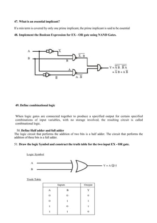
= AB'C + ACC' + A'BB' + A'BC' + BB'C + BCC' = AB'C + A'BC'
35. Show that (X + Y' + XY)( X + Y')(X'Y) = 0
(X + Y' + XY)( X + Y')(X'Y) = (X + Y' + X)(X + Y' )(X' + Y) [A + A'B = A + B]
= (X + Y' )(X + Y' )(X'Y) [A + A = 1]
= (X + Y' )(X'Y) [A.A = 1]
= X.X' + Y'.X'.Y
= 0 [A.A' = 0]
36. Prove that ABC + ABC' + AB'C + A'BC = AB + AC + BC
ABC + ABC' + AB'C + A'BC=AB(C + C') + AB'C + A'BC
=AB + AB'C + A'BC
=A(B + B'C) + A'BC
=A(B + C) + A'BC
=AB + AC + A'BC
=B(A+C)+AC
=AB + BC + AC
=AB + AC +BC ...Proved
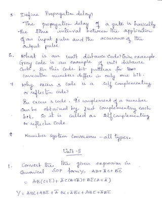
37. Convert the given expression in canonical SOP form Y = AC + AB + BC
Y = AC + AB + BC
=AC(B + B' ) + AB(C + C' ) + (A + A')BC
=ABC + ABC' + AB'C + AB'C' + ABC + ABC' + ABC
=ABC + ABC' +AB'C + AB'C' [A + A =1]
38. Define duality property.
Duality property states that every algebraic expression deducible from the postulates of Boolean
algebra remains valid if the operators and identity elements are interchanged. If the dual of an
algebraic expression is desired, we simply interchange OR and AND operators and replace 1's by 0's
and 0's by 1's.
39. Find the complement of the functions F1 = x'yz' + x'y'z and F2 = x(y'z' + yz). By
applying De-Morgan's theorem.
F1' = (x'yz' + x'y'z)' = (x'yz')'(x'y'z)' = (x + y' + z)(x + y +z')](https://image.slidesharecdn.com/ee8351-dlc-190816093101/85/EE8351-DLC-6-320.jpg)
![7
F2' = [x(y'z' + yz)]' = x' + (y'z' + yz)'
= x' + (y'z')'(yz)'
= x' + (y + z)(y' + z')
40. Simplify the following expression
Y = (A + B) (A = C) (B + C)
= (A A + A C + A B + B C) (B + C) = (A C + A B + B C) (B + C)
= A B C + A C C + A B B + A B C + B B C + B C C = A B C
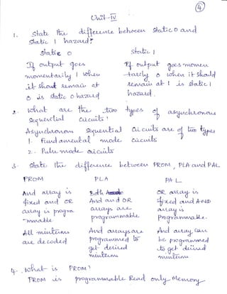
41. What are the methods adopted to reduce Boolean function?
i) Karnaug map
ii) Tabular method or Quine Mc-Cluskey method
iii) Variable entered map technique.
42. State the limitations of karnaugh map.
i) Generally it is limited to six variable map (i.e) more then six variable involving expression
are not reduced.
ii) The map method is restricted in its capability since they are useful for simplifying only
Boolean expression represented in standard form.
What is a karnaugh map?
A karnaugh map or k map is a pictorial form of truth table, in which the map diagram is made up of
squares, with each squares representing one minterm of the function.
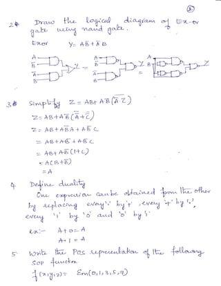
43. Find the minterms of the logical expression Y = A'B'C' + A'B'C + A'BC + ABC'
Y = A'B'C' + A'B'C + A'BC + ABC'
=m0 + m1 +m3 +m6
=∑m(0, 1, 3, 6)
44. Write the maxterms corresponding to the logical expression
Y = (A + B + C' )(A + B' + C')(A' + B' + C)
= (A + B + C' )(A + B' + C')(A' + B' + C) =M1.M3.M6
=π M(1,3,6)
45. What are called don’t care conditions?
In some logic circuits certain input conditions never occur, therefore the corresponding
output never appears. In such cases the output level is not defined, it can be either high or low. These
output levels are indicated by ‘X’ or‘d’ in the truth tables and are called don’t care conditions or
incompletely specified functions.
46. What is a prime implicant?
A prime implicant is a product term obtained by combining the maximum possible number of
adjacent squares in the map.](https://image.slidesharecdn.com/ee8351-dlc-190816093101/85/EE8351-DLC-7-320.jpg)

![o
t.
o
9
E76zol -DfflU l-rff. C>riB
P^"L=A
U'"-,. [- e
Cunv Q"* _tt^{-
ft"T uA-z
lrtk*f brwar,l c"Au i',^1, a-
1 g r o I I I ao>q
l+Otttq tldtot*D
Yu I I t o D I 0o
A3 cn-l-,-io ltll looloo
l4: ,y:*tr'Jrr*-,u o)^+ic. q^b.
#; t lh-- 'rqa^)J"^
"vLL,^Le')
tl a#*'g"ffii,ffi*#T*-"0
sp.-fl.J -ir:,,dlz
3,v..-f ,^-^R, to f-^^ y"t," o.'.tP*tr' *^^J effu CA)--,-br
o.Jt*-fl
"I-dh.*^ p rV epe*^ ..t{""l;v
I ,+.^L *ft V6+ eil?*L *fi--""fut
p*Il"f .^""4
tf"ll ip^rt- *-*"? p*J-l ,],.-o'. rr-^^^r"t'{
lTe--)^Alqfu
Xare
s,q*ry ry.*a'u*r-'$* ffi eP**A t^
lF. Giu<. -t-* **^^^fW fu k-...S't"lA"I coA,^t
gqil, 2-,;2-t ; "x^^1'^
"
4- u^*"^5't^D2"l d'' '](https://image.slidesharecdn.com/ee8351-dlc-190816093101/85/EE8351-DLC-25-320.jpg)
![{. Gn"-r- IL,
La,AV cl
I
U"?U-g'---
,r^^&u;*b-
9p- fi -f-f tt p
eq--t-tt0
@
e<voflio.* ^-r^.)
c-1,^ooa&ur..lr.
)
$*^"-^"h^i L..- 7v'-b*^
of,[Ltr) -- S+E o'tt)
O
I
o
1
,o
l
O
I
e
O
O
o
t
t
I
I
o
0
I
-ri^JP-tr^***-b-
9"+*k dra^"#^ A**
tr ^4t"*
ofb-,I?*t
W?r..-L L fffi A^a^.A^cI t^^ Rs liupp*n
W Rs #^ft-t"f ,re** bA|"- 1'-f"-lr a-,,--e:.
l, or^}p"I ., i*N'
'
,rUoJ- L^ 4-Y- a)x;f&',
1.,^
gVM a:*;V,tar'*r^b 16 -'";tr**? b''^- l 'td^"o
{" "^;* d*"-
14'D e')
fu '?h *4 "L ; a-
J.^r^.-b ^,- A Y""^"--V
aeML" e+
r'^ g^)"*'wt"AJ
dxt'-[t,*L & & +'*'i;^^*-.t
r>, a)a,^] d'ild"" *J
L ?-'"'^Y
t'^fJ'
v^,+.x
Iffi;T,4{"+ ,8. o- 4
+U- oit//ut't''-'
'
3'
t"](https://image.slidesharecdn.com/ee8351-dlc-190816093101/85/EE8351-DLC-29-320.jpg)
![.k^r^^e g "^'-''n*bT,.4
cvrrpt r.,Le,r- 4. -"[P "-[-
u ^14
@,.*+ bk"^^^ +-*^:'"'
?* w-o-" a- Art r,{'---t- tF
-$".*
i+u-' ro'6 Jz ^'^)
1*b"
-,,-r p*[- *f"'u.al
"-"^e
rnl-
I
;*A U5 "rYflL4t'L'4-Ye
Arr-coA- .-t-'t '"n'-^'z^"-
Y*T*vv'il-lt-
SR*
Y4?t'r I
k.,irJ
s- c-*^^-f a'a2 4*'-?^f'
Full"- "t^tA-
'Ci)-c-IL-^-^ T '
I t'"^F--lfc{i-'Ld dJ'/v
=11"- i.*ftr.L Ya,r- o*U-'t'
d"d ^ff- o"'t* d""^
t-t^z- c''xu^L
(
Lt gU'LbL'
"*t
o"4- i"^f* ca'-rx
d,a,^f ''Fo
t^*-
&^.h--b a'2-2- )e-/&4
eA .,"-t- d'""
}...^*c bl""A- e3" ^ 1 Pla
ntt^oA* cn-";-lt ^*d
P,ild-Q,
fL-r-J+' -{ th" pwl^"' *
^n
g r^*& +"- IF'-
;,{;t t- L-'P''^J 6-1'
a""*--;)* W- [f.'
--"; L*.r^J 6-lk-
t -^4"-E
[ "'
'*-[d
]-# o Qi]'L^2
V"Y't-' *Vr
u@,,.-4'"o*cy^p{ f.rn1u-H; wo-^'
b1&uk fa-"-'tr dJ&6 u'e-P- fA"'^
i")"-A oVvd>
6
rlr +fDci"i-C.L{tulhvt
+1p h",-"?](https://image.slidesharecdn.com/ee8351-dlc-190816093101/85/EE8351-DLC-32-320.jpg)
![:-l * r"rt,^-U aq.-a-- llL
eLilV^r^-u*,
tir C^*-"A A'vo d*f- *yY"u^I
Ct) O^- t"r{' il"*k- *ff'r*/*}'
8 " r-?..J- a-arz- rdLcr-& )
h#,'2^ dr" cr(- ^^flx- 9+r)g, vax-'a)-llA
d^fl*Ar* ,u-r*l,roAn
I d-b@
@""-- *l
tr-."1,S{*-b- utolU.
VA*^-r- ,l^" A.t:lotts* t, Ct^a""
41tu{ drls / v^c-(- e-^Aj}*^ ,"ff^ ."
t^-*o1"^l dA^^tr , ik *^r't Car^A-z-
k ,V"^f -r-i" crJU tt'^"yr-A^c)-^LA
,)raCt: a,^t- q
n
l,-" r-
C{ib cAyau'. Ik-^+ ^"-l d-Ju "4*-lz A-f
"A^C{ib c;lya(z'^ 4 |k-^'tr-:r"af ila}V s-e=W, drf -
6r, lt^:f arr')-rrt t't( uuY" d,- 11,6, s|.,e vaila-Llk-
c-fvi1-LyLO-t
1
d""^"tr, . lt- cwa. Cs- C^rt,r-Ji h -^ L ttea^r+4^I , .rt- .-s
CrU a) cr.'-, h c-.) Ya' ct' '
Var,.,t ila-
Crn C. il,
ur^J.-.At -,
Vr*^^il€r^-b
A ora a^^^t
r^,,or^* Qr,rttC T a'c-o.i
%lk- 1-{--f
gf."bL.-"*=.}., A,,*
^*
AA e,^A.o en^ lhr- orA-ro eL^ uo],; 21* Ik- g+*-Pd
d@"**f , ltro- )e-cz-'t's rytg,Y b.o*^^.$..i- "
1,of"-* L4 a-
%'1"2
A Cyc,t- oc.):,'-e *'?^t-- a',"#^o)'^xpvturL
rvoka/> r.t- )"il'/wih^^ *9'*-*-^6'[^ o u g€'-t]
+
?r^Lvz '
uot..--l' o.t,a.- V"r^^an
l*qz-^A* cisLe LLLilrea^^-MA -gr"aF-).;?
1ru ^fF* ^+ lt=*- oAT,+-
ILe-c^u"-
I ItL pro ?nJ'.,,- )A^f
)o"](https://image.slidesharecdn.com/ee8351-dlc-190816093101/85/EE8351-DLC-33-320.jpg)
![,rY!1
r. hdt*l- tt v1;D L 1
.V *e t-- ,r^r& 1n,.'34" 4,"A W?-^-E3 e-t c';]'
l;*../ v)o*-o- 'beo*pi*- )*"V7"* ik .s *4
-16 Mrufuu &tfU e*o^ila Ln k^l Po''nu-
Dtfl ; &; *il*
-
c# L' s''rM)Ae'A *"5'/++oL'
b?'"A ef."^'V", RJ^A"'"^i
"*+
' 'NtL""-"-b.
,f;^It^ a^^-J c-"..-F,,.n.-I* '1'*t+-'
Lol^^tr L^ o ?n"h-^tr
dL" v++ PL
i 7^cka,y-U ^c-l'l,ufr*'4 A-+"bf1el,
,*l-*r^,b' ,
'C.r,',-t'<-"t
"b , +*A'* a^d f'oo
Yrd
6"ul.'ur-t^ , f"D clAlr-),a-
A,-t-t"-^"-$'oA^ '
tol.aJ. at-a- tk-- n'-x-[ c^/-^ .n"l'c,
.l+p r-
Je"}'-, 1,w" d^
$.-l- {-t-'-
>r)"avi rrA
9+*^c+."'^-a.,1
o
,.
A
q
P. l'
,.
f)
keaib th- LJ.-vro-o) """"odJ I
D dtrfkg:
J5loyaan i <-e2-',
l^t.t- i.e--e--o-. sH *VT.- Tl t q,"LU
€^.trtT DFF u,s
Pa+C D, t)L, ru** I Li^ gpl-V.,"
)
cr,.'ilc,'* s+d-€,
<-r.A DF€
atc0;t= &5^. t.l.-^,orr,-r-*.1 cyf pFF u
Leq;^ )
P'rt, er*o L dV
L<a*;
'rl" gn;y.'t' +f,,^
'*.= o
d,,*$ edlc=r)pr_._nd
ruQc=D)
.*.a {,](https://image.slidesharecdn.com/ee8351-dlc-190816093101/85/EE8351-DLC-34-320.jpg)
![L
"1-
v ,^l.,, +r-* *,.oAn-l a# c*LLe-g [.-*, fa e^"rc;]
*fr^"aL +-- ?r-,"" 1t{" }Y'e b lk -""}""}-
-Tl^,a-
^'i-PS
sl-,tz '*{-'}5 cvutL . "^-A h'
At,- ciV<- 'u* ap<-^'c-b""^^
% lk-,. c'ic,;L oL^*e*
A.d tu. t[,- Y*T-^-*-
Lc* [z v.i+D L cnA,(- +* 2X I rr,ur-r-x
'{ :-3c'* sg(
)^bx*"rl i e-oz ;
r^^-r- i e;. r4-l-L6'.
-r I 6q . *-t {;
e-.fi-tr1 l"-u_,t)L t
0
P""t- Lsrf , ,T, : & sl-d -tr b. )
Y: c'** sH-bf)
€*d rrrtur j
a "t.;
b..l^^. "^&,*y,,a,qx-
t-4
b"o.*
Yu.= (q^,,+ s) a''d %
+ S arxd2, )
I
e,VC )
sf*h. ril- -- v"^Ii"4i 4 , paoVaXt- A'4""-*"*
Sre.,", C*Ia-^^b A''-dc.-La-|-.''or"n 2
A oar*.q q/-, .^r & c*W*A"ev- 4. d+^& YA'A gc.r-ha
f- "^J & cxyr-,d.'"c7v- 4. aax-a't*Vry^
rr ^- " ,L,,^ I= C rnzr.r-D ."t^k , &!^"4-^,^. *^^--f
r--
'h-^b , c-ovuuP *nP-^k '+hqq4^J Cp,,q_1,@wv , , | ''l*-'
U A I-^ I"-^. A f rn,t-rf:o
*.
C-a,txp*A"^L b t
I n F l-.](https://image.slidesharecdn.com/ee8351-dlc-190816093101/85/EE8351-DLC-35-320.jpg)