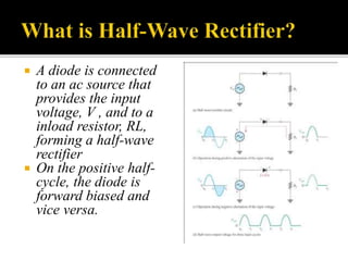
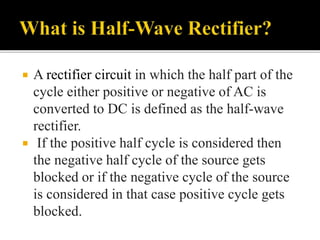
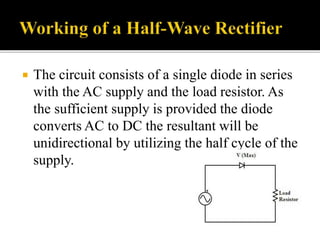
Course code: 402
Course title: Modern Physics & Electronics
Course Incharge: Sehrish Inam, Lecturer Physics
 A diode is connected
to an ac source that
provides the input
voltage, V , and to a
inload resistor, RL,
forming a half-wave
rectifier
 On the positive half-
cycle, the diode is
forward biased and
vice versa.
 A rectifier circuit in which the half part of the
cycle either positive or negative of AC is
converted to DC is defined as the half-wave
rectifier.
 If the positive half cycle is considered then
the negative half cycle of the source gets
blocked or if the negative cycle of the source
is considered in that case positive cycle gets
blocked.
 The circuit consists of a single diode in series
with the AC supply and the load resistor. As
the sufficient supply is provided the diode
converts AC to DC the resultant will be
unidirectional by utilizing the half cycle of the
supply.
 In positive half cycle sufficient amount of voltage
reaches the diode resulting it to function in
forwarding bias condition.
 The process of rectification occurs at the load
resistance where the generated voltage in the
circuit is consumed by the load.
 Load resistor is to block the excess current
produced in the circuit due to the diode.
 Here the positive side of the supply is considered
so it is termed as a positive half-wave rectifier.
 Here the diode direction is changed so it
begins to conduct during the applied negative
supply of the voltage and the positive cycle
gets blocked.
 The current produced in the circuit gets
measured at the load resistor.
 The output generated consists of pulsating Dc
but the intention of rectification is to produce
constant DC.
• RMSValue of a Half-Wave Rectifier
• RMS is defined as the root mean square value. For
load current, the RMS value can be given as
• IRMS = Im/2
• The RMS value of the output voltage is given as
• VRMS = IRMS RL
• VRMS = Im/2 * RL
 The efficiency of the rectifier is the ratio
between the generated output power to the
applied input power.
 E = Pdc / Pac
 The maximum efficiency produced is 40.6%.
 Question: if input signal is being rectified half,
then why the efficiency is not 50%?
 The output produced consists of pulsating DC.
 Pulses in the output referred to as ripples.
 The number of ripples present at the output
can be measured in terms of ripple factor.
 Ripple Factor, γ =(Ripple voltage at the output)
( dc output voltage )
This ripple factor effects the practical
implementation of half wave rectifier.
 Requirements list of the components is less.
 The cost for the construction is low.
 Less number of components presence results
in the construction of rectifier in the easiest
manner.
 It is simple to analyze because the designed
circuit is straight forward.
 The output generated in this rectifier is in the
form of pulses.
 The ripple factor is high.
 Results in the power loss of the circuit.
 The transformer utilization factor (TUF) of the
half-wave rectifier is low.
 Here the output generated requires the filter to
be connected across the load because of the
ripples generated at the output voltage.
 The requirement of generating dc output
voltage paves the way for the application of
the half-wave rectifier circuit with the filter
attached across the load.
 In the power supplies circuitry where the
constant DC at the output is not considered as
the major requirement at that case, the half-
wave rectifier can be used.
Course code: 402
Course title: Modern Physics & Electronics
Course Incharge: Sehrish Inam, Lecturer Physics
 A rectifier that utilizes both the positive and
the negative half of the input cycle and
undergoes rectification is defined as a full-
wave rectifier.
 The full-wave bridge rectifier uses four
diodes, as shown on the next slide
 For +ve input cycle (a), diodes D1 and D4 are
forward-biased and conduct current, while diodes
D2 and D3 are reverse-biased
 For –ve input cycle (b), diodes D2 and D3 are
forward-biased and conduct current, while diodes
D1 and D4 are reverse-biased
 The full-wave rectifier can be designed by
using with a minimum of two basic diodes or
it can use four diodes based on the topology
suggested.
 Full-wave rectifier can be classified into two
types. They are
(1) Center – Tapped
A center-tapped full-wave rectifier circuit
consists of two diodes, a transformer, and a
resistive load.
 A center-tapped transformer is a normal
transformer that has a slight modification in it.
Its secondary winding has a wire connected at
the center. Hence the input supply AC voltage
while passing through the secondary winding
its voltage is divided into two halves. The one
half is referred to positive half of the voltage.
Whereas the remaining half of the voltage is
for the negative part of the cycle.
 The circuit consists
of two diodes that
are connected in
parallel to each
other along with the
resistive load. The
load is connected at
the center-tapped
wire of the
secondary winding.
 The input is provided to the center-tapped
transformer as it reaches the secondary
winding the voltage is divided into two halves.
During the positive half of the input cycles,
the diode D1 is in forwarding bias condition
indicating the conducting mode and the diode
D2 is in the non-conducting mode because it is
in reverse bias condition. The flow of
current is observed at the terminal of diode
D1.
 During the negative half of the cycle, the
diode D2 conducts because of the center-
tapped transformer property and the diode D1
is in reverse bias condition that is in non-
conduction mode. During this consequence the
terminal at D2 one can find the flow of current
through it and at D1 there is no evident flow
of current or the current is blocked at D1
terminal.
 Hence both the cycles are utilized here for
rectification without any loss of input power.
 The average output voltage of the half-wave
rectifier is doubled compared to that of the
half-wave rectifier.
 A full-wave bridge rectifying circuit consists
of four diodes connected in a diagonal manner
that is nothing but in bridge topology.
 No center-tapped transformer is used.
 The four diodes connected in a bridge form.
 Diagonally opposite diodes conduct during
one half of the cycle.
 Second half the remaining two diode
conducts.
 The diode D1 and D4 are diagonally opposite to
each other whereas D2 and D3 are also
connected in a diagonally opposite manner.
During this the diodes D1 and D4 are in
forwarding bias condition that is in conduction
mode acts like closed switch then the path is
established for the flow of current. Whereas
diodes D2 and D3 are in reverse bias mode.
 As the negative cycle of the supply reaches the
bridge rectifying circuit diodes D1 and D4
becomes reverse bias and the diodes D2 and D3
act in forwarding bias mode. Hence the path is
established for the flow of current between
and D3. Where D1 and D4 diodes act like an
open circuit and block the flow of current
 The full-wave rectifier has more efficiency compared
to that of a half-wave rectifier.
 There is the utilization of both the cycles. Hence there
is no loss in the output power.
 As both the cycles used in rectification. There will be
no loss in the input voltage signal.
 Ripple factor is less compared to that of the half-wave
rectifier.
 Greater mean in DC value is achieved.
 Compare to the center-tapped full-wave rectifier bridge
rectifier is cost-effective because the center-tapped is
more costly.
 The only disadvantage of this circuit is that
the center-tapped transformer utilized here is
costly.
 To overcome this disadvantage bridge
rectifier circuit is constructed where the four
diodes are connected in a bridge topology.
 The amplitude for the modulating radio signal is
detected using the full-wave bridge rectifier circuit.
 In electric wielding to supply steady DC voltage in a
polarized way, this circuit is preferred.
 As the efficiency of rectification is high in this rectifier
circuit, it is used in various appliances as a part of the
power supply unit.
 It has the capability of converting high AC voltage to
low DC value.
 In case of powering up of the devices like motors and
LED devices these are used.
Halfwave and full wave rectificaton

Halfwave and full wave rectificaton

  • 1.
    Course code: 402 Coursetitle: Modern Physics & Electronics Course Incharge: Sehrish Inam, Lecturer Physics
  • 2.
     A diodeis connected to an ac source that provides the input voltage, V , and to a inload resistor, RL, forming a half-wave rectifier  On the positive half- cycle, the diode is forward biased and vice versa.
  • 3.
     A rectifiercircuit in which the half part of the cycle either positive or negative of AC is converted to DC is defined as the half-wave rectifier.  If the positive half cycle is considered then the negative half cycle of the source gets blocked or if the negative cycle of the source is considered in that case positive cycle gets blocked.
  • 4.
     The circuitconsists of a single diode in series with the AC supply and the load resistor. As the sufficient supply is provided the diode converts AC to DC the resultant will be unidirectional by utilizing the half cycle of the supply.
  • 5.
     In positivehalf cycle sufficient amount of voltage reaches the diode resulting it to function in forwarding bias condition.  The process of rectification occurs at the load resistance where the generated voltage in the circuit is consumed by the load.  Load resistor is to block the excess current produced in the circuit due to the diode.  Here the positive side of the supply is considered so it is termed as a positive half-wave rectifier.
  • 6.
     Here thediode direction is changed so it begins to conduct during the applied negative supply of the voltage and the positive cycle gets blocked.  The current produced in the circuit gets measured at the load resistor.  The output generated consists of pulsating Dc but the intention of rectification is to produce constant DC.
  • 8.
    • RMSValue ofa Half-Wave Rectifier • RMS is defined as the root mean square value. For load current, the RMS value can be given as • IRMS = Im/2 • The RMS value of the output voltage is given as • VRMS = IRMS RL • VRMS = Im/2 * RL
  • 9.
     The efficiencyof the rectifier is the ratio between the generated output power to the applied input power.  E = Pdc / Pac  The maximum efficiency produced is 40.6%.  Question: if input signal is being rectified half, then why the efficiency is not 50%?
  • 10.
     The outputproduced consists of pulsating DC.  Pulses in the output referred to as ripples.  The number of ripples present at the output can be measured in terms of ripple factor.  Ripple Factor, γ =(Ripple voltage at the output) ( dc output voltage ) This ripple factor effects the practical implementation of half wave rectifier.
  • 11.
     Requirements listof the components is less.  The cost for the construction is low.  Less number of components presence results in the construction of rectifier in the easiest manner.  It is simple to analyze because the designed circuit is straight forward.
  • 12.
     The outputgenerated in this rectifier is in the form of pulses.  The ripple factor is high.  Results in the power loss of the circuit.  The transformer utilization factor (TUF) of the half-wave rectifier is low.  Here the output generated requires the filter to be connected across the load because of the ripples generated at the output voltage.
  • 13.
     The requirementof generating dc output voltage paves the way for the application of the half-wave rectifier circuit with the filter attached across the load.  In the power supplies circuitry where the constant DC at the output is not considered as the major requirement at that case, the half- wave rectifier can be used.
  • 15.
    Course code: 402 Coursetitle: Modern Physics & Electronics Course Incharge: Sehrish Inam, Lecturer Physics
  • 16.
     A rectifierthat utilizes both the positive and the negative half of the input cycle and undergoes rectification is defined as a full- wave rectifier.
  • 17.
     The full-wavebridge rectifier uses four diodes, as shown on the next slide  For +ve input cycle (a), diodes D1 and D4 are forward-biased and conduct current, while diodes D2 and D3 are reverse-biased  For –ve input cycle (b), diodes D2 and D3 are forward-biased and conduct current, while diodes D1 and D4 are reverse-biased
  • 19.
     The full-waverectifier can be designed by using with a minimum of two basic diodes or it can use four diodes based on the topology suggested.  Full-wave rectifier can be classified into two types. They are (1) Center – Tapped A center-tapped full-wave rectifier circuit consists of two diodes, a transformer, and a resistive load.
  • 20.
     A center-tappedtransformer is a normal transformer that has a slight modification in it. Its secondary winding has a wire connected at the center. Hence the input supply AC voltage while passing through the secondary winding its voltage is divided into two halves. The one half is referred to positive half of the voltage. Whereas the remaining half of the voltage is for the negative part of the cycle.
  • 21.
     The circuitconsists of two diodes that are connected in parallel to each other along with the resistive load. The load is connected at the center-tapped wire of the secondary winding.
  • 22.
     The inputis provided to the center-tapped transformer as it reaches the secondary winding the voltage is divided into two halves. During the positive half of the input cycles, the diode D1 is in forwarding bias condition indicating the conducting mode and the diode D2 is in the non-conducting mode because it is in reverse bias condition. The flow of current is observed at the terminal of diode D1.
  • 23.
     During thenegative half of the cycle, the diode D2 conducts because of the center- tapped transformer property and the diode D1 is in reverse bias condition that is in non- conduction mode. During this consequence the terminal at D2 one can find the flow of current through it and at D1 there is no evident flow of current or the current is blocked at D1 terminal.
  • 24.
     Hence boththe cycles are utilized here for rectification without any loss of input power.  The average output voltage of the half-wave rectifier is doubled compared to that of the half-wave rectifier.
  • 25.
     A full-wavebridge rectifying circuit consists of four diodes connected in a diagonal manner that is nothing but in bridge topology.  No center-tapped transformer is used.
  • 27.
     The fourdiodes connected in a bridge form.  Diagonally opposite diodes conduct during one half of the cycle.  Second half the remaining two diode conducts.
  • 28.
     The diodeD1 and D4 are diagonally opposite to each other whereas D2 and D3 are also connected in a diagonally opposite manner. During this the diodes D1 and D4 are in forwarding bias condition that is in conduction mode acts like closed switch then the path is established for the flow of current. Whereas diodes D2 and D3 are in reverse bias mode.
  • 29.
     As thenegative cycle of the supply reaches the bridge rectifying circuit diodes D1 and D4 becomes reverse bias and the diodes D2 and D3 act in forwarding bias mode. Hence the path is established for the flow of current between and D3. Where D1 and D4 diodes act like an open circuit and block the flow of current
  • 30.
     The full-waverectifier has more efficiency compared to that of a half-wave rectifier.  There is the utilization of both the cycles. Hence there is no loss in the output power.  As both the cycles used in rectification. There will be no loss in the input voltage signal.  Ripple factor is less compared to that of the half-wave rectifier.  Greater mean in DC value is achieved.  Compare to the center-tapped full-wave rectifier bridge rectifier is cost-effective because the center-tapped is more costly.
  • 31.
     The onlydisadvantage of this circuit is that the center-tapped transformer utilized here is costly.  To overcome this disadvantage bridge rectifier circuit is constructed where the four diodes are connected in a bridge topology.
  • 32.
     The amplitudefor the modulating radio signal is detected using the full-wave bridge rectifier circuit.  In electric wielding to supply steady DC voltage in a polarized way, this circuit is preferred.  As the efficiency of rectification is high in this rectifier circuit, it is used in various appliances as a part of the power supply unit.  It has the capability of converting high AC voltage to low DC value.  In case of powering up of the devices like motors and LED devices these are used.