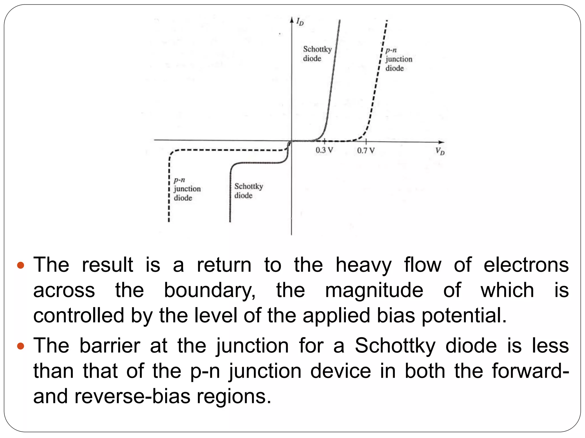
This document provides information about PN junction diodes and their characteristics:
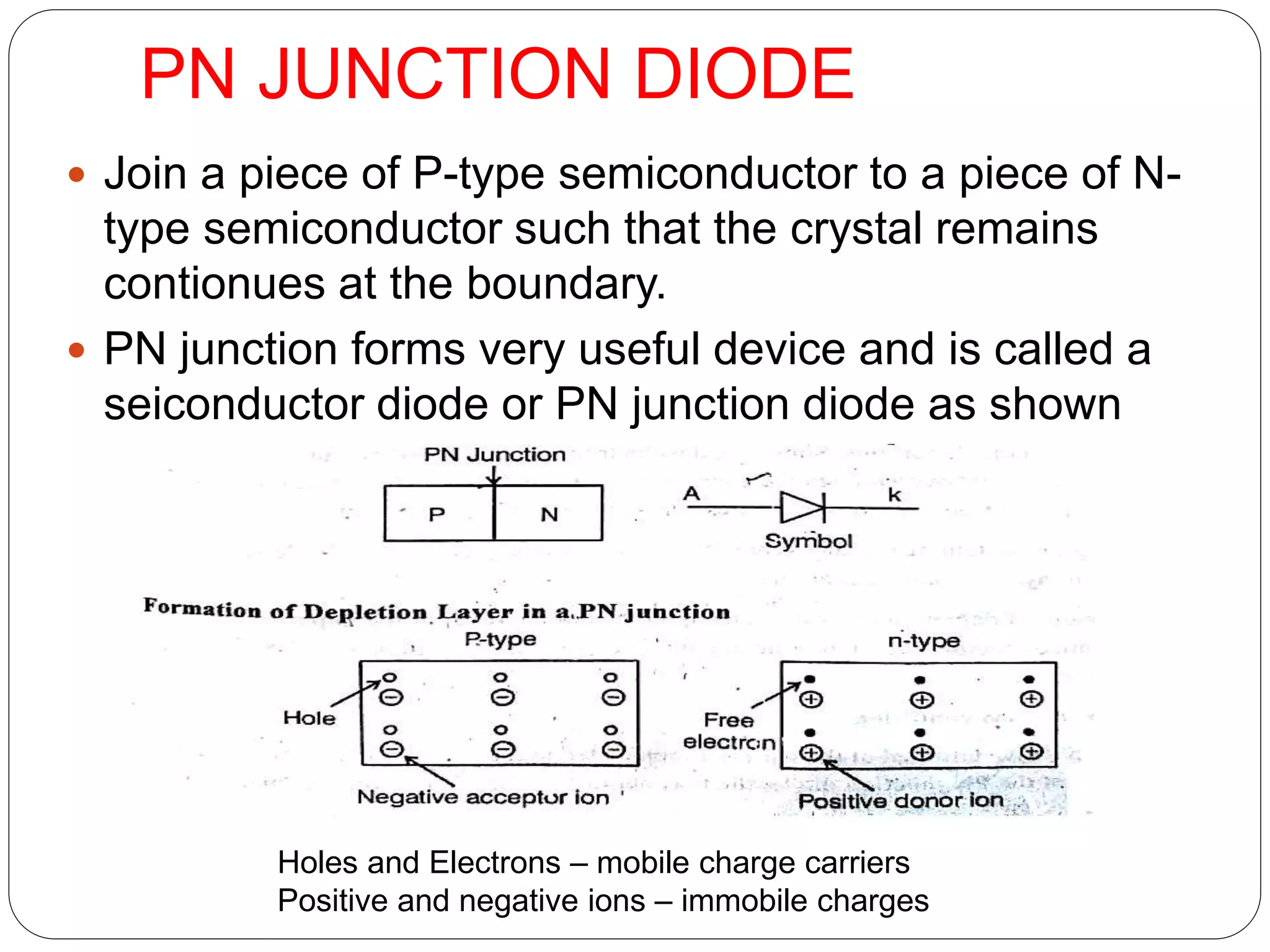
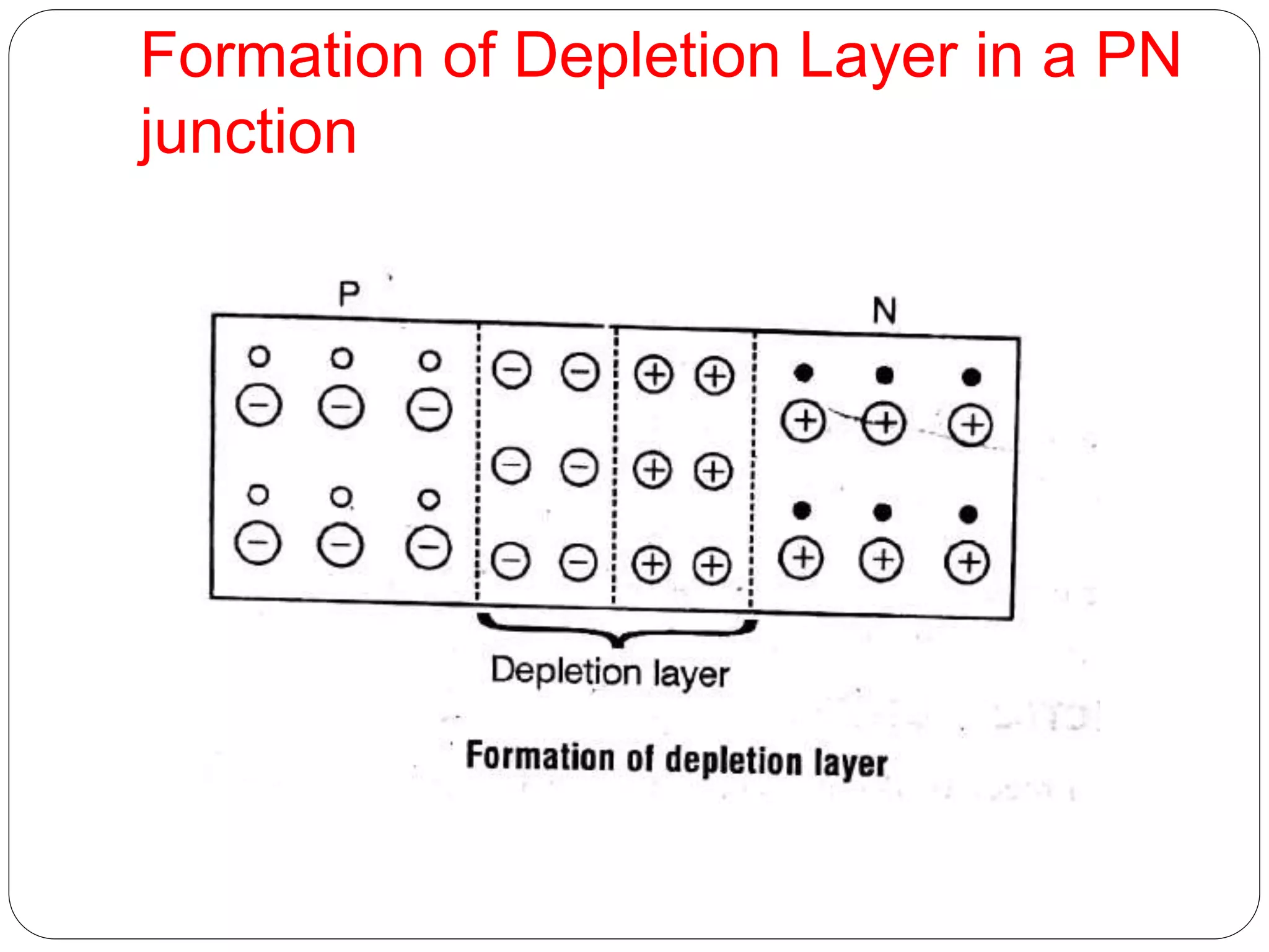
1) It describes how a PN junction is formed by combining P-type and N-type semiconductors, forming a depletion region.
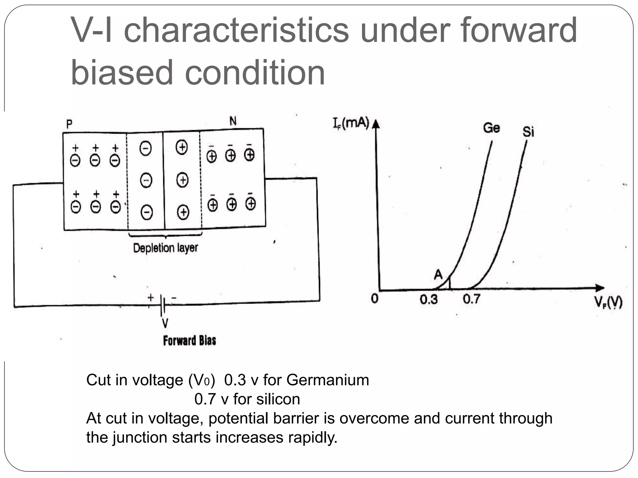
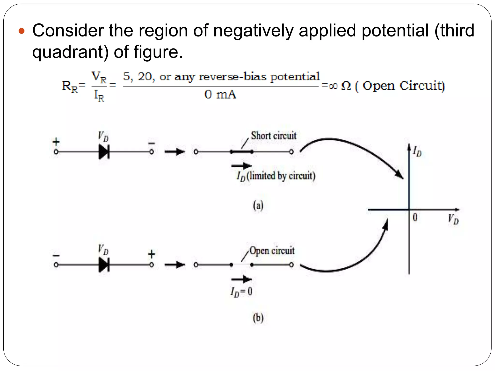
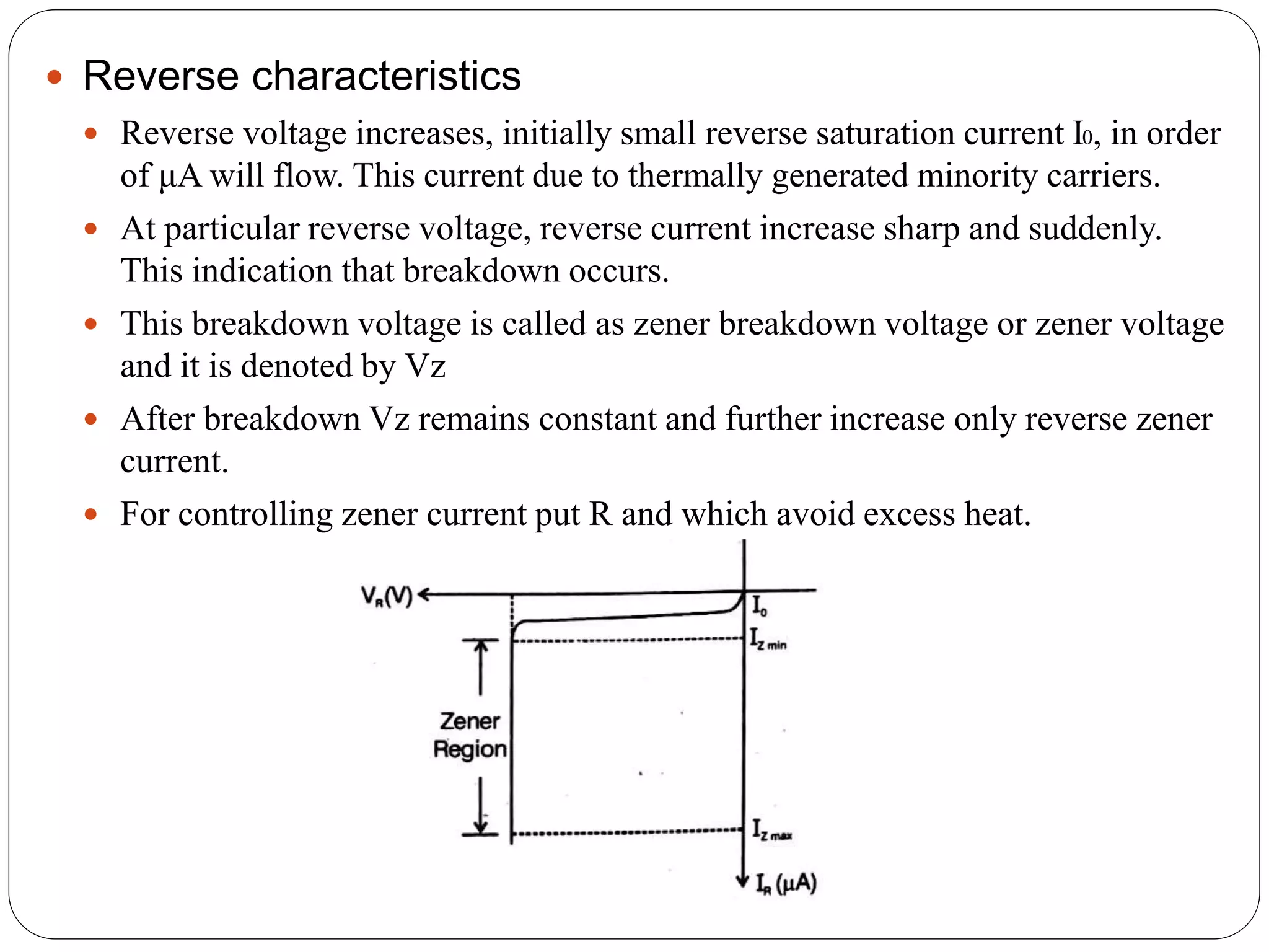
2) It explains the I-V characteristics of a diode under forward and reverse bias, including how the depletion region changes with bias.
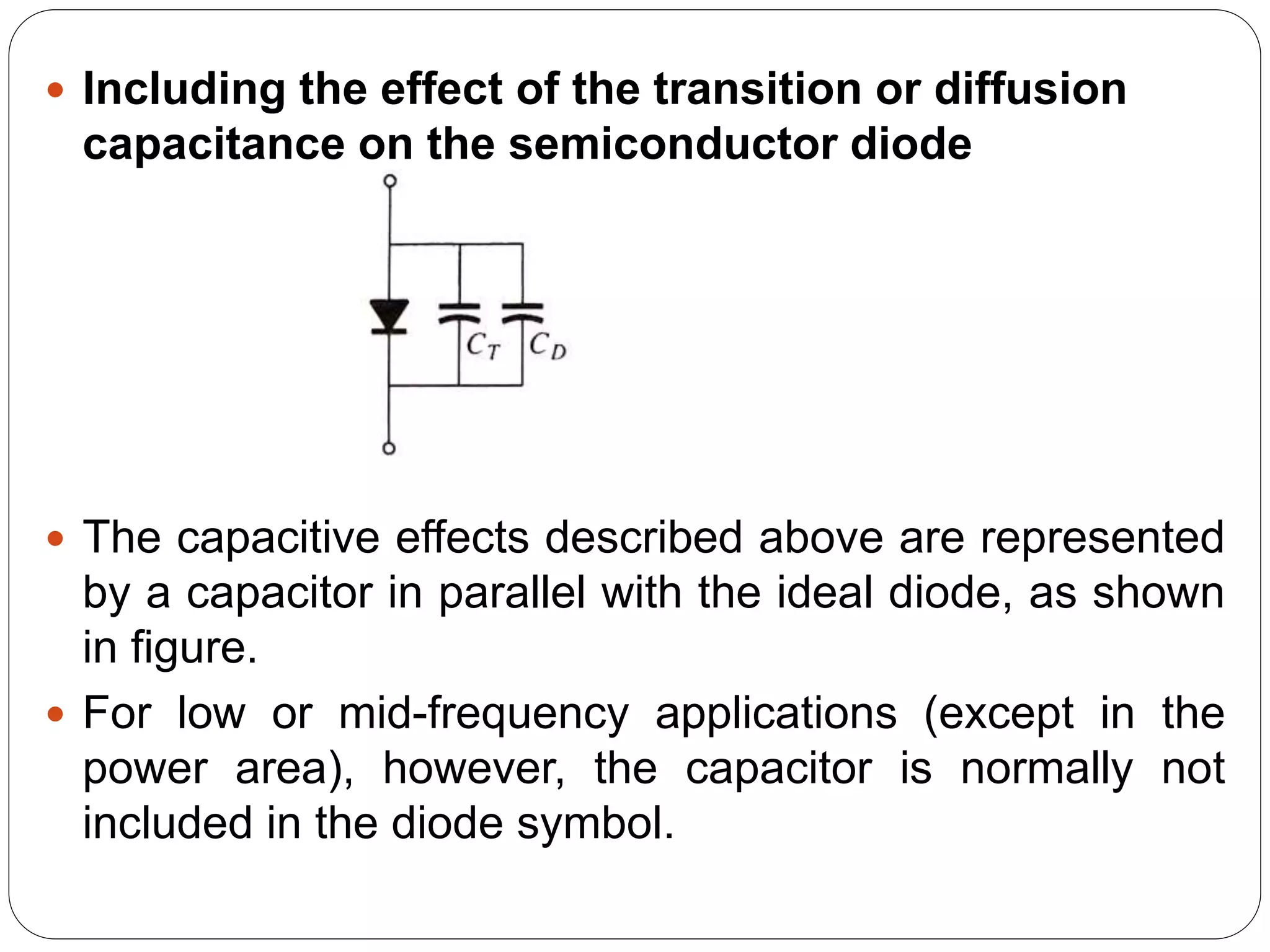
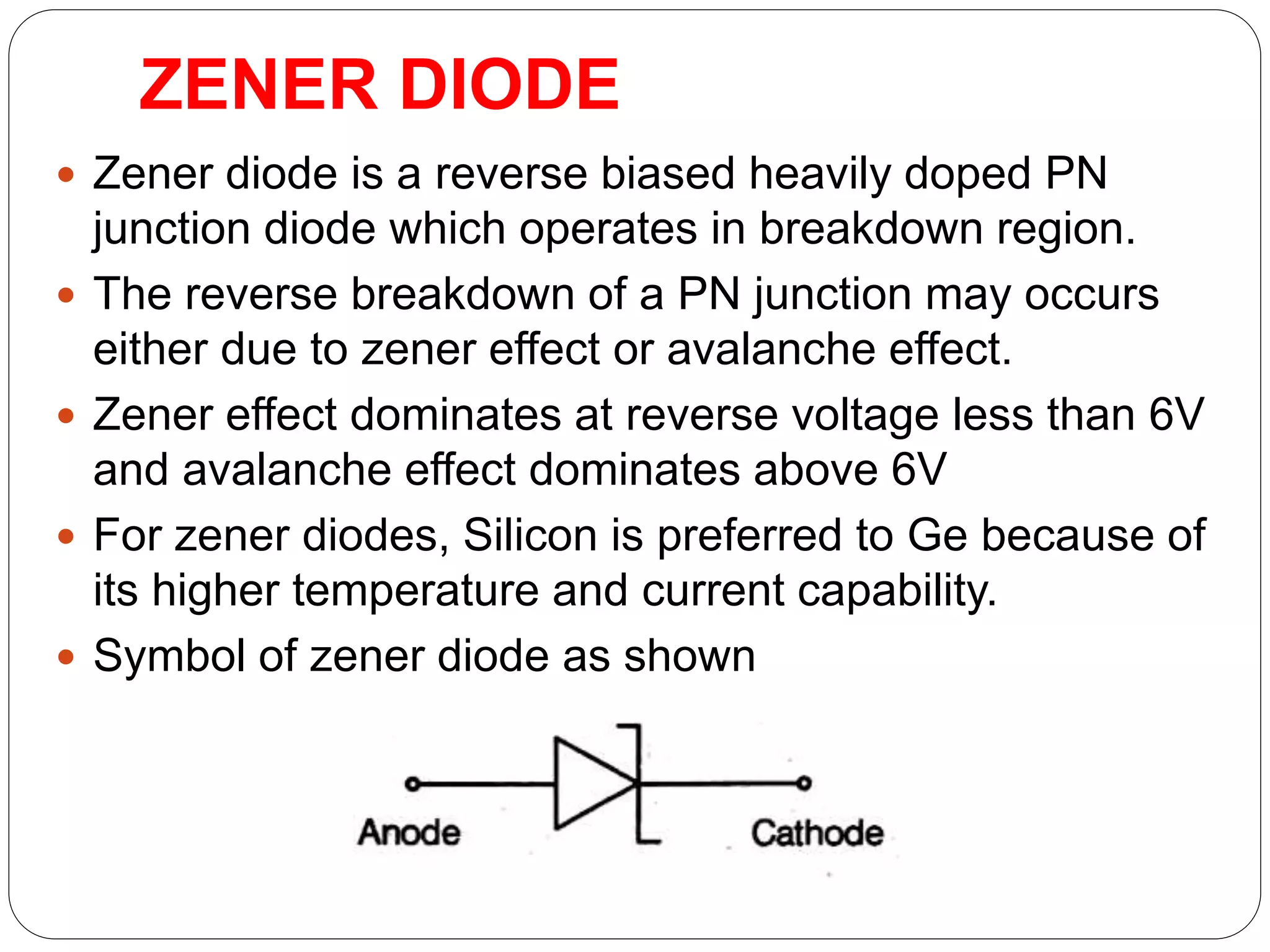
3) Additional topics covered include drift and diffusion currents, temperature effects, capacitance effects, and recovery time characteristics important for switching applications. Special diodes like Zener diodes are also introduced.


![VARACTOR (VARICAP)
DIODES
Varactor [also called varicap, VVC (voltage-variable
capacitance), or tuning] diodes are semiconductor,
voltage-dependent, variable capacitors.
Their mode of operation depends on the capacitance
that exists at the p-n junction when the element is
reverse-biased.
Under reverse-bias conditions, it was established that
there is a region of uncovered charge on either side of
the junction that together the regions make up the
depletion region and define the depletion width Wd.
The transition capacitance (CT) established by the
isolated uncovered charges is determined by](https://image.slidesharecdn.com/aeuniti-230818092735-694f0c27/75/AE-UNIT-I-ppt-69-2048.jpg)