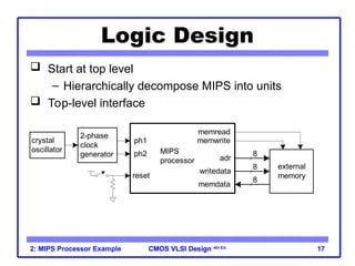
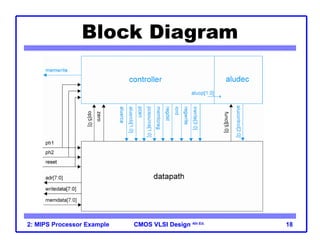
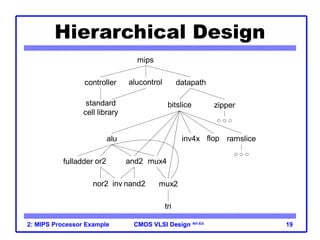
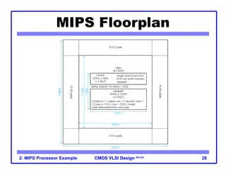
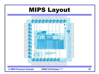
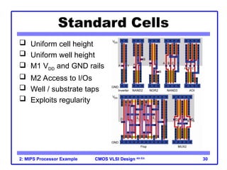
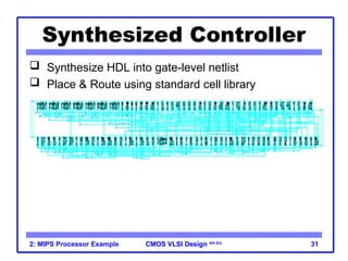
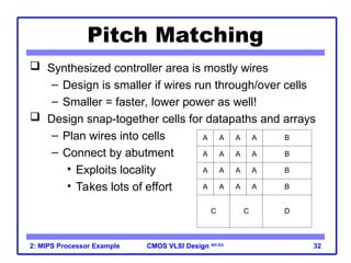
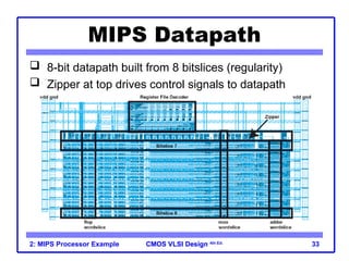
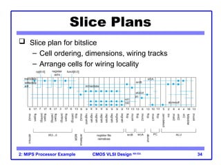
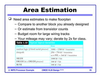
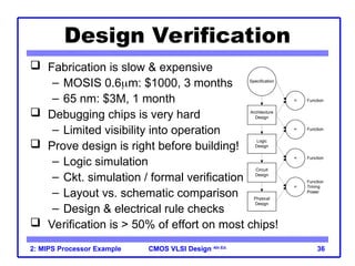
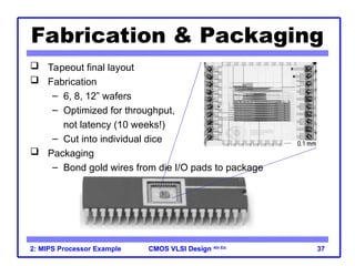
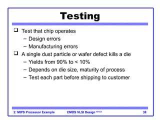
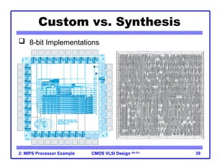
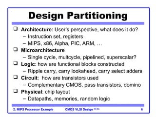
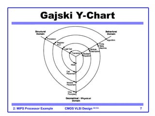
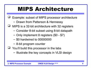
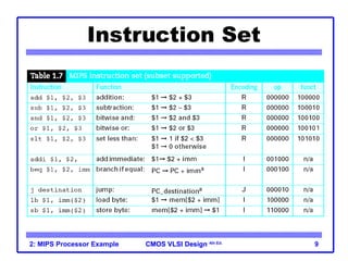
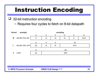
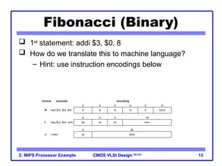
This document outlines a lecture on the design of a MIPS processor using CMOS VLSI design, covering topics from architecture to physical design. It includes details on structured design, microarchitecture, logic design, and the steps involved in fabrication and testing. The MIPS processor example serves to illustrate key concepts in digital design and hardware description languages.


![CMOS VLSI Design
CMOS VLSI Design 4th Ed.
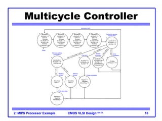
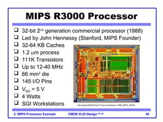
2: MIPS Processor Example 15
MIPS Microarchitecture
Multicycle architecture ( [Paterson04], [Harris07] )](https://image.slidesharecdn.com/lect2-mipsex-240914085156-4d985c67/85/MIPS-processor-in-VLSI-design-Processor-design-15-320.jpg)