The document discusses CMOS transistor theory, including:
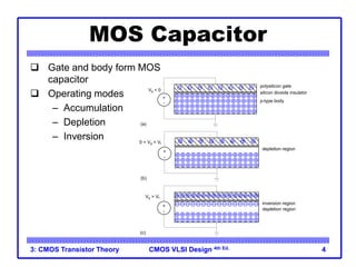
1) It describes the MOS capacitor structure and its operating modes of accumulation, depletion, and inversion.
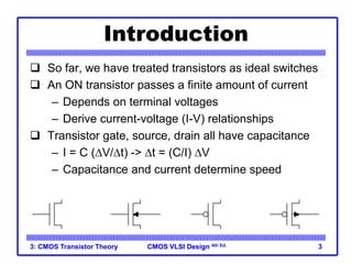
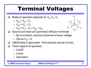
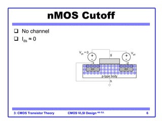
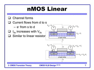
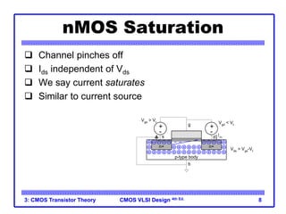
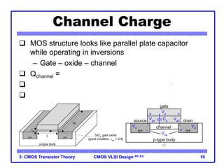
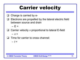
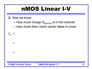
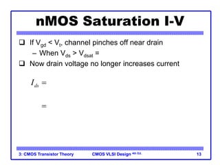
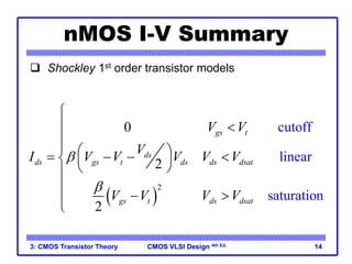
2) It analyzes the I-V characteristics of nMOS and pMOS transistors in the cutoff, linear, and saturation regions based on the channel charge and carrier velocity.
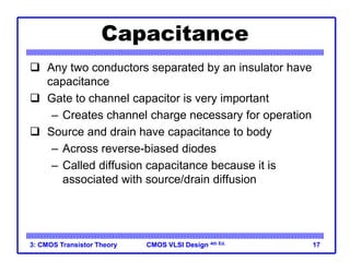
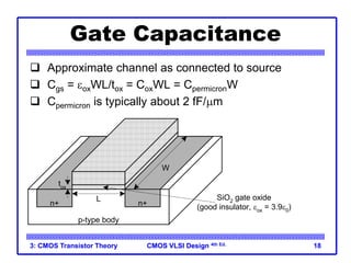
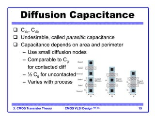
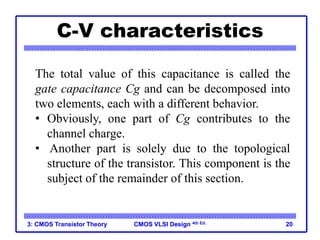
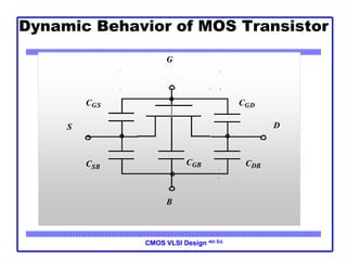
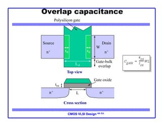
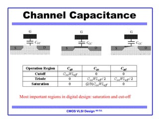
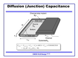
3) It explains the gate, source, and drain capacitances of MOS transistors and how they impact speed. The gate capacitance contributes to channel charge while other capacitances are parasitic.