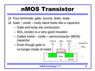
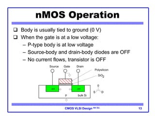
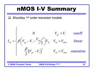
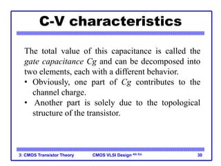
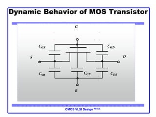
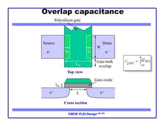
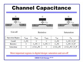
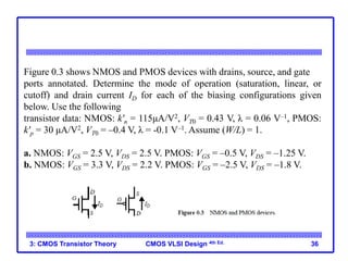
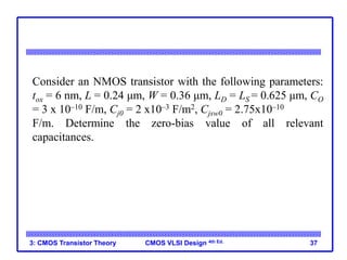
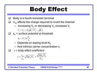
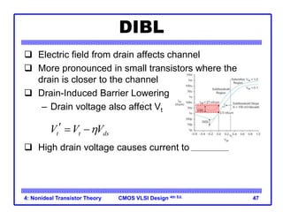
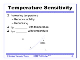
SlideShare a Scribd company logo
CMOS VLSI Design 4th Ed.
VLSI System
Design(BECE303L)
Dr. Satheesh Kumar S
Cabin: TT(A)-102-G
Mobile: 8124424714
CMOS VLSI Design 4th Ed.
VLSI Design Overview
and MOSFET Theory
2
CMOS VLSI Design 4th Ed.
Electrical Numerical Integrator And Calculator (ENIAC).
CMOS VLSI Design 4th Ed.
What is VLSI ?
Very Large Scale Integration
Integration: Integrated Circuits (Within IC).
 Multiple Devices in a substrate
 How Large is Very Large?
 SSI (Small Scale Integration)
 10 to 100 transistors (7400 series)
 MSI (Medium Scale)
 100 to 1000 transistors (74000 series)
 LSI (Large Scale)
 1000 to 10000 transistors
 VLSI (Very Large Scale)
 > 10000 transistors
 ULSI (Ultra Large Scale)
 (Not so popular)
CMOS VLSI Design 4th Ed.
VLSI Design Flow
CMOS VLSI Design 4th Ed.
2: MIPS Processor Example 9
Structured Design
 Hierarchy: Divide and Conquer
– Recursively system into modules
 Regularity
– Decomposition of a large system in simple and
similar blocks as much as possible.
– Reuse modules wherever possible
– Ex: Standard cell library
CMOS VLSI Design 4th Ed.
 Modularity: well-formed interfaces
– Modularity in design means that the various
functional blocks which make up the larger
system must have well-defined functions and
interfaces.
– Modularity allows that each block or module can
be designed relatively independently from each
other.
– All of the blocks can be combined with ease at
the end of the design process, to form the large
system.
10
CMOS VLSI Design 4th Ed.
– The concept of modularity enables the
parallelisation of the design process.
– Allows modules to be treated as black boxes
 Locality
– The concept of locality also ensures that
connections are mostly between neighboring
modules, avoiding long-distance connections as
much as possible.
– Physical and temporal
11
CMOS VLSI Design 4th Ed. 12
nMOS Transistor
 Four terminals: gate, source, drain, body
 Gate – oxide – body stack looks like a capacitor
– Gate and body are conductors
– SiO2 (oxide) is a very good insulator
– Called metal – oxide – semiconductor (MOS)
capacitor
– Even though gate is
no longer made of metal
n+
p
Gate
Source Drain
bulk Si
SiO2
Polysilicon
n+
Body
CMOS VLSI Design 4th Ed. 13
nMOS Operation
 Body is usually tied to ground (0 V)
 When the gate is at a low voltage:
– P-type body is at low voltage
– Source-body and drain-body diodes are OFF
– No current flows, transistor is OFF
n+
p
Gate
Source Drain
bulk Si
SiO2
Polysilicon
n+
D
0
S
CMOS VLSI Design 4th Ed. 14
polysilicon gate
(a)
silicon dioxide insulator
p-type body
+
-
Vg < 0
MOS Capacitor
 Gate and body form MOS
capacitor
 Operating modes
– Accumulation
– Depletion
– Inversion
(b)
+
-
0 < Vg < Vt
depletion region
(c)
+
-
Vg > Vt
depletion region
inversion region
CMOS VLSI Design 4th Ed. 15
Terminal Voltages
 Mode of operation depends on Vg, Vd, Vs
– Vgs = Vg – Vs
– Vgd = Vg – Vd
– Vds = Vd – Vs = Vgs - Vgd
 Source and drain are symmetric diffusion terminals
– By convention, source is terminal at lower voltage
– Hence Vds  0
 nMOS body is grounded. First assume source is 0 too.
 Three regions of operation
– Cutoff
– Linear
– Saturation
Vg
Vs
Vd
Vgd
Vgs
Vds
+
-
+
-
+
-
CMOS VLSI Design 4th Ed. 16
nMOS Cutoff
 No channel
 Ids ≈ 0
+
-
Vgs
= 0
n+ n+
+
-
Vgd
p-type body
b
g
s d
CMOS VLSI Design 4th Ed. 17
nMOS Linear
 Channel forms
 Current flows from d to s
– e- from s to d
 Ids increases with Vds
 Similar to linear resistor
+
-
Vgs
> Vt
n+ n+
+
-
Vgd
= Vgs
+
-
Vgs
> Vt
n+ n+
+
-
Vgs
> Vgd
> Vt
Vds
= 0
0 < Vds
< Vgs
-Vt
p-type body
p-type body
b
g
s d
b
g
s d
Ids
CMOS VLSI Design 4th Ed. 18
nMOS Saturation
 Channel pinches off
 Ids independent of Vds
 We say current saturates
 Similar to current source
+
-
Vgs
> Vt
n+ n+
+
-
Vgd
< Vt
Vds
> Vgs
-Vt
p-type body
b
g
s d Ids
CMOS VLSI Design 4th Ed. 19
Ideal I-V Characteristics
 In Linear region, Ids depends on
– How much charge is in the channel?
– How fast is the charge moving?
CMOS VLSI Design 4th Ed.
3: CMOS Transistor Theory 20
Channel Charge
 MOS structure looks like parallel plate capacitor
while operating in inversions
– Gate – oxide – channel
 Qchannel = CV
 C = Cg = eoxWL/tox = CoxWL
 V = Vgc – Vt = (Vgs – Vds/2) – Vt
n+ n+
p-type body
+
Vgd
gate
+ +
source
-
Vgs
-
drain
Vds
channel
-
Vg
Vs
Vd
Cg
n+ n+
p-type body
W
L
tox
SiO2
gate oxide
(good insulator, eox
= 3.9)
polysilicon
gate
Cox = eox / tox
CMOS VLSI Design 4th Ed.
 Vgc- vt = amount of voltage attracting charge to the
channel beyond the minimum required to invert from
P to n.
21
CMOS VLSI Design 4th Ed.
3: CMOS Transistor Theory 22
Carrier velocity
 Charge is carried by e-
 Electrons are propelled by the lateral electric field
between source and drain
– E = Vds/L
 Carrier velocity v proportional to lateral E-field
– v = mE m called mobility
 Time for carrier to cross channel:
– t = L / v
CMOS VLSI Design 4th Ed.
3: CMOS Transistor Theory 23
nMOS Linear I-V
 Now we know
– How much charge Qchannel is in the channel
– How much time t each carrier takes to cross
channel
ox 2
2
ds
ds
gs t ds
ds
gs t ds
Q
I
t
W V
C V V V
L
V
V V V
m


 
  
 
 
 
  
 
 
ox
=
W
C
L
 m
CMOS VLSI Design 4th Ed.
3: CMOS Transistor Theory 24
nMOS Saturation I-V
 If Vgd < Vt, channel pinches off near drain
– When Vds > Vdsat = Vgs – Vt
 Now drain voltage no longer increases current
 
2
2
2
dsat
ds gs t dsat
gs t
V
I V V V
V V


 
  
 
 
 
CMOS VLSI Design 4th Ed.
3: CMOS Transistor Theory 25
nMOS I-V Summary
 
2
cutoff
linear
saturatio
0
2
2
n
gs t
ds
ds gs t ds ds dsat
gs t ds dsat
V V
V
I V V V V V
V V V V



 

  
   
 

 


 


 Shockley 1st order transistor models
CMOS VLSI Design 4th Ed. 26
pMOS Transistor
 Similar, but doping and voltages reversed
– Body tied to high voltage (VDD)
– Gate low: transistor ON
– Gate high: transistor OFF
– Bubble indicates inverted behavior
SiO2
n
Gate
Source Drain
bulk Si
Polysilicon
p+ p+
CMOS VLSI Design 4th Ed. 27
Transistors as Switches
 We can view MOS transistors as electrically
controlled switches
 Voltage at gate controls path from source to drain
g
s
d
g = 0
s
d
g = 1
s
d
g
s
d
s
d
s
d
nMOS
pMOS
OFF
ON
ON
OFF
CMOS VLSI Design 4th Ed.
3: CMOS Transistor Theory 28
Capacitance
 Any two conductors separated by an insulator have
capacitance
 Gate to channel capacitor is very important
– Creates channel charge necessary for operation
 Source and drain have capacitance to body
– Across reverse-biased diodes
– Called diffusion capacitance because it is
associated with source/drain diffusion
CMOS VLSI Design 4th Ed.
3: CMOS Transistor Theory 29
Gate Capacitance
 Approximate channel as connected to source
 Cgs = eoxWL/tox = CoxWL = CpermicronW
 Cpermicron is typically about 2 fF/mm
n+ n+
p-type body
W
L
tox
SiO2
gate oxide
(good insulator, eox
= 3.9e0
)
polysilicon
gate
CMOS VLSI Design 4th Ed.
C-V characteristics
3: CMOS Transistor Theory 30
The total value of this capacitance is called the
gate capacitance Cg and can be decomposed into
two elements, each with a different behavior.
• Obviously, one part of Cg contributes to the
channel charge.
• Another part is solely due to the topological
structure of the transistor.
CMOS VLSI Design 4th Ed.
Dynamic Behavior of MOS Transistor
D
S
G
B
CGD
CGS
CSB CDB
CGB
CMOS VLSI Design 4th Ed.
Overlap capacitance
tox
n+ n+
Cross section
L
Gate oxide
xd xd
Ld
Polysilicon gate
Top view
Gate-bulk
overlap
Source
n+
Drain
n+
W
CMOS VLSI Design 4th Ed.
Channel Capacitance
S D
G
CGC
S D
G
CGC
S D
G
CGC
Cut-off Resistive Saturation
Most important regions in digital design: saturation and cut-off
CMOS VLSI Design 4th Ed.
Channel Capacitance
WLCox
WLCox
2
2WLCox
3
CGC
CGCS
VDS /(VGS-VT)
CGCD
0 1
CGC
CGCS = CGCD
CGC B
WLCox
WLCox
2
VGS
Capacitance as a function of VGS
(with VDS = 0)
Capacitance as a function of the
degree of saturation
CMOS VLSI Design 4th Ed.
Diffusion (Junction) Capacitance
Bottom
Side wall
Side wall
Channel
Source
ND
Channel-stop implant
N
A1
SubstrateNA
W
xj
L S
CMOS VLSI Design 4th Ed.
3: CMOS Transistor Theory 36
Figure 0.3 shows NMOS and PMOS devices with drains, source, and gate
ports annotated. Determine the mode of operation (saturation, linear, or
cutoff) and drain current ID for each of the biasing configurations given
below. Use the following
transistor data: NMOS: k'n = 115μA/V2, VT0 = 0.43 V, λ = 0.06 V–1, PMOS:
k'p = 30 μA/V2, VT0 = –0.4 V, λ = -0.1 V–1. Assume (W/L) = 1.
a. NMOS: VGS = 2.5 V, VDS = 2.5 V. PMOS: VGS = –0.5 V, VDS = –1.25 V.
b. NMOS: VGS = 3.3 V, VDS = 2.2 V. PMOS: VGS = –2.5 V, VDS = –1.8 V.
CMOS VLSI Design 4th Ed.
3: CMOS Transistor Theory 37
Consider an NMOS transistor with the following parameters:
tox = 6 nm, L = 0.24 μm, W = 0.36 μm, LD = LS = 0.625 μm, CO
= 3 x 10⁻¹⁰ F/m, Cj0 = 2 x10⁻³ F/m2, Cjsw0 = 2.75x10⁻¹⁰
F/m. Determine the zero-bias value of all relevant
capacitances.
CMOS VLSI Design 4th Ed.
3: CMOS Transistor Theory 38
Solution:
CMOS VLSI Design 4th Ed.
4: Nonideal Transistor Theory 39
Non-ideal Transistor Theory
 Nonideal Transistor Behavior
– High Field Effects
• Mobility Degradation
• Velocity Saturation
– Channel Length Modulation
– Threshold Voltage Effects
• Body Effect
• Drain-Induced Barrier Lowering
• Short Channel Effect
– Leakage
• Subthreshold Leakage
• Gate Leakage
• Junction Leakage
CMOS VLSI Design 4th Ed.
4: Nonideal Transistor Theory 40
Channel Length Modulation
 Reverse-biased p-n junctions form a depletion region
– Region between n and p with no carriers
– Width of depletion Ld region grows with reverse bias
– Leff = L – Ld
 Shorter Leff gives more current
– Ids increases with Vds
– Even in saturation
n
+
p
Gate
Source Drain
bulk Si
n
+
VDD
GND VDD
GND
L
Leff
Depletion Region
Width: Ld
CMOS VLSI Design 4th Ed.
4: Nonideal Transistor Theory 41
Chan Length Mod I-V
 l = channel length modulation coefficient
– not feature size
– Empirically fit to I-V characteristics
   
2
1
2
ds gs t ds
I V V V

l
  
CMOS VLSI Design 4th Ed.
4: Nonideal Transistor Theory 42
Ideal vs. Simulated nMOS I-V Plot
 65 nm IBM process, VDD = 1.0 V
0 0.2 0.4 0.6 0.8 1
0
200
400
600
800
1000
1200
Vds
Ids (mA)
Vgs = 1.0
Vgs = 1.0
Vgs = 0.8
Vgs = 0.6
Vgs = 0.4
Vgs = 0.8
Vgs = 0.6
Channel length modulation:
Saturation current increases
with Vds
Ion = 747 mA @
Vgs = Vds = VDD
Simulated
Ideal
Velocity saturation & Mobility degradation:
Saturation current increases less than
quadratically with Vgs
Velocity saturation & Mobility degradation:
Ion lower than ideal model predicts
CMOS VLSI Design 4th Ed.
4: Nonideal Transistor Theory 43
Electric Fields Effects
 Vertical electric field: Evert = Vgs / tox
– Attracts carriers into channel
– Long channel: Qchannel  Evert
 Lateral electric field: Elat = Vds / L
– Accelerates carriers from drain to source
– Long channel: v = mElat
CMOS VLSI Design 4th Ed.
4: Nonideal Transistor Theory 44
Velocity Saturation
 At high Elat, carrier velocity rolls off
– Carriers scatter off atoms in silicon lattice
– Velocity reaches vsat
• Electrons: 107 cm/s
• Holes: 8 x 106 cm/s
– Better model
CMOS VLSI Design 4th Ed.
4: Nonideal Transistor Theory 45
Threshold Voltage Effects
 Vt is Vgs for which the channel starts to invert
 Ideal models assumed Vt is constant
 Really depends (weakly) on almost everything else:
– Body voltage: Body Effect
– Drain voltage: Drain-Induced Barrier Lowering
– Channel length: Short Channel Effect
CMOS VLSI Design 4th Ed.
4: Nonideal Transistor Theory 46
Body Effect
 Body is a fourth transistor terminal
 Vsb affects the charge required to invert the channel
– Increasing Vs or decreasing Vb increases Vt
 fs = surface potential at threshold
– Depends on doping level NA
– And intrinsic carrier concentration ni
 g = body effect coefficient
 
0
t t s sb s
V V V
g f f
   
2 ln A
s T
i
N
v
n
f 
si
ox
si
ox ox
2q
2q A
A
N
t
N
C
e
g e
e
 
CMOS VLSI Design 4th Ed.
4: Nonideal Transistor Theory 47
DIBL
 Electric field from drain affects channel
 More pronounced in small transistors where the
drain is closer to the channel
 Drain-Induced Barrier Lowering
– Drain voltage also affect Vt
 High drain voltage causes current to increase.
ttdsVVV
t t ds
V V V

  
CMOS VLSI Design 4th Ed.
4: Nonideal Transistor Theory 48
Temperature Sensitivity
 Increasing temperature
– Reduces mobility
– Reduces Vt
 ION decreases with temperature
 IOFF increases with temperature
Vgs
ds
I
increasing
temperature

More Related Content

Similar to FALLSEM2023-24_BECE303L_TH_VL2023240100242_2023-04-24_Reference-Material-I.ppt

EC6601 VLSI Design CMOS Fabrication
EC6601 VLSI Design   CMOS FabricationEC6601 VLSI Design   CMOS Fabrication
EC6601 VLSI Design CMOS Fabrication
chitrarengasamy
 
MOS-Nonideal charecteristics
MOS-Nonideal charecteristicsMOS-Nonideal charecteristics
MOS-Nonideal charecteristics
Shanmuga Raju
 
VLSI- Unit I
VLSI- Unit IVLSI- Unit I
VLSI- Unit I
MADHUMITHA154
 
lect00_introducao of Very large scale Integration Tech .ppt
lect00_introducao of Very large scale Integration Tech .pptlect00_introducao of Very large scale Integration Tech .ppt
lect00_introducao of Very large scale Integration Tech .ppt
gixem51910
 
Power
PowerPower
Power
AnimSarker
 
2016 ch4 delay
2016 ch4 delay2016 ch4 delay
2016 ch4 delay
hdainghia194
 
VLSI Design_ Stick Diagrams_slidess.pptx
VLSI Design_ Stick Diagrams_slidess.pptxVLSI Design_ Stick Diagrams_slidess.pptx
VLSI Design_ Stick Diagrams_slidess.pptx
bansalnamz
 
Introduction to VLSI Technology
Introduction to VLSI TechnologyIntroduction to VLSI Technology
Introduction to VLSI Technology
Dr.YNM
 
EEE 4157_Lecture_10_11_12_13.ppt
EEE 4157_Lecture_10_11_12_13.pptEEE 4157_Lecture_10_11_12_13.ppt
EEE 4157_Lecture_10_11_12_13.ppt
OmarFaruqe23
 
Lect 1 - cktlay.ppt
Lect 1 - cktlay.pptLect 1 - cktlay.ppt
Lect 1 - cktlay.ppt
AnimSarker
 
lect1-circuits and layout.ppt
lect1-circuits and layout.pptlect1-circuits and layout.ppt
lect1-circuits and layout.ppt
ssuserf7da1a
 
20EC602 VLSI Design.ppt
20EC602 VLSI Design.ppt20EC602 VLSI Design.ppt
20EC602 VLSI Design.ppt
ASureshkumar13
 
Mos transistor
Mos transistorMos transistor
Mos transistor
Murali Rai
 
Very Large Scale Integration -VLSI
Very Large Scale Integration -VLSIVery Large Scale Integration -VLSI
Very Large Scale Integration -VLSIPRABHAHARAN429
 
EEE 4157_Lecture_7_8_9.ppt
EEE 4157_Lecture_7_8_9.pptEEE 4157_Lecture_7_8_9.ppt
EEE 4157_Lecture_7_8_9.ppt
OmarFaruqe23
 
Vlsi design notes(1st unit) according to vtu syllabus.(BE)
Vlsi  design notes(1st unit) according to vtu syllabus.(BE)Vlsi  design notes(1st unit) according to vtu syllabus.(BE)
Vlsi design notes(1st unit) according to vtu syllabus.(BE)
instrumentation_vtu
 
EMT529-VLSI-Design-wk1.pdf
EMT529-VLSI-Design-wk1.pdfEMT529-VLSI-Design-wk1.pdf
EMT529-VLSI-Design-wk1.pdf
Fazrul Faiz Zakaria
 
lect0-intro.ppt
lect0-intro.pptlect0-intro.ppt
lect0-intro.ppt
NickYu23
 
Lect 0 - intro.ppt
Lect 0 - intro.pptLect 0 - intro.ppt
Lect 0 - intro.ppt
AnimSarker
 
Lecture 9.ppt
Lecture 9.pptLecture 9.ppt
Lecture 9.ppt
TimePresents
 

Similar to FALLSEM2023-24_BECE303L_TH_VL2023240100242_2023-04-24_Reference-Material-I.ppt (20)

EC6601 VLSI Design CMOS Fabrication
EC6601 VLSI Design   CMOS FabricationEC6601 VLSI Design   CMOS Fabrication
EC6601 VLSI Design CMOS Fabrication
 
MOS-Nonideal charecteristics
MOS-Nonideal charecteristicsMOS-Nonideal charecteristics
MOS-Nonideal charecteristics
 
VLSI- Unit I
VLSI- Unit IVLSI- Unit I
VLSI- Unit I
 
lect00_introducao of Very large scale Integration Tech .ppt
lect00_introducao of Very large scale Integration Tech .pptlect00_introducao of Very large scale Integration Tech .ppt
lect00_introducao of Very large scale Integration Tech .ppt
 
Power
PowerPower
Power
 
2016 ch4 delay
2016 ch4 delay2016 ch4 delay
2016 ch4 delay
 
VLSI Design_ Stick Diagrams_slidess.pptx
VLSI Design_ Stick Diagrams_slidess.pptxVLSI Design_ Stick Diagrams_slidess.pptx
VLSI Design_ Stick Diagrams_slidess.pptx
 
Introduction to VLSI Technology
Introduction to VLSI TechnologyIntroduction to VLSI Technology
Introduction to VLSI Technology
 
EEE 4157_Lecture_10_11_12_13.ppt
EEE 4157_Lecture_10_11_12_13.pptEEE 4157_Lecture_10_11_12_13.ppt
EEE 4157_Lecture_10_11_12_13.ppt
 
Lect 1 - cktlay.ppt
Lect 1 - cktlay.pptLect 1 - cktlay.ppt
Lect 1 - cktlay.ppt
 
lect1-circuits and layout.ppt
lect1-circuits and layout.pptlect1-circuits and layout.ppt
lect1-circuits and layout.ppt
 
20EC602 VLSI Design.ppt
20EC602 VLSI Design.ppt20EC602 VLSI Design.ppt
20EC602 VLSI Design.ppt
 
Mos transistor
Mos transistorMos transistor
Mos transistor
 
Very Large Scale Integration -VLSI
Very Large Scale Integration -VLSIVery Large Scale Integration -VLSI
Very Large Scale Integration -VLSI
 
EEE 4157_Lecture_7_8_9.ppt
EEE 4157_Lecture_7_8_9.pptEEE 4157_Lecture_7_8_9.ppt
EEE 4157_Lecture_7_8_9.ppt
 
Vlsi design notes(1st unit) according to vtu syllabus.(BE)
Vlsi  design notes(1st unit) according to vtu syllabus.(BE)Vlsi  design notes(1st unit) according to vtu syllabus.(BE)
Vlsi design notes(1st unit) according to vtu syllabus.(BE)
 
EMT529-VLSI-Design-wk1.pdf
EMT529-VLSI-Design-wk1.pdfEMT529-VLSI-Design-wk1.pdf
EMT529-VLSI-Design-wk1.pdf
 
lect0-intro.ppt
lect0-intro.pptlect0-intro.ppt
lect0-intro.ppt
 
Lect 0 - intro.ppt
Lect 0 - intro.pptLect 0 - intro.ppt
Lect 0 - intro.ppt
 
Lecture 9.ppt
Lecture 9.pptLecture 9.ppt
Lecture 9.ppt
 

More from VijaySathappan

task33_ppt.pptx
task33_ppt.pptxtask33_ppt.pptx
task33_ppt.pptx
VijaySathappan
 
task31.pptx
task31.pptxtask31.pptx
task31.pptx
VijaySathappan
 
t17_1.pptx
t17_1.pptxt17_1.pptx
t17_1.pptx
VijaySathappan
 
t14_1.pptx
t14_1.pptxt14_1.pptx
t14_1.pptx
VijaySathappan
 
TASK16.pptx
TASK16.pptxTASK16.pptx
TASK16.pptx
VijaySathappan
 
8951019.ppt
8951019.ppt8951019.ppt
8951019.ppt
VijaySathappan
 
t17_1.pptx
t17_1.pptxt17_1.pptx
t17_1.pptx
VijaySathappan
 
task 8.pptx
task 8.pptxtask 8.pptx
task 8.pptx
VijaySathappan
 
task13.pptx
task13.pptxtask13.pptx
task13.pptx
VijaySathappan
 
task 7.pptx
task 7.pptxtask 7.pptx
task 7.pptx
VijaySathappan
 
task 1.pptx
task 1.pptxtask 1.pptx
task 1.pptx
VijaySathappan
 
FALLSEM2023-24_BSTS301P_SS_VL2023240100008_2023-05-24_Reference-Material-I.pptx
FALLSEM2023-24_BSTS301P_SS_VL2023240100008_2023-05-24_Reference-Material-I.pptxFALLSEM2023-24_BSTS301P_SS_VL2023240100008_2023-05-24_Reference-Material-I.pptx
FALLSEM2023-24_BSTS301P_SS_VL2023240100008_2023-05-24_Reference-Material-I.pptx
VijaySathappan
 
txt to ppt(1).ppt
txt to ppt(1).ppttxt to ppt(1).ppt
txt to ppt(1).ppt
VijaySathappan
 
task 6.ppt
task 6.ppttask 6.ppt
task 6.ppt
VijaySathappan
 
FALLSEM2023-24_BECE302L_TH_VL2023240100270_2023-05-04_Reference-Material-I.pptx
FALLSEM2023-24_BECE302L_TH_VL2023240100270_2023-05-04_Reference-Material-I.pptxFALLSEM2023-24_BECE302L_TH_VL2023240100270_2023-05-04_Reference-Material-I.pptx
FALLSEM2023-24_BECE302L_TH_VL2023240100270_2023-05-04_Reference-Material-I.pptx
VijaySathappan
 
New Microsoft PowerPoint Presentation.pptx
New Microsoft PowerPoint Presentation.pptxNew Microsoft PowerPoint Presentation.pptx
New Microsoft PowerPoint Presentation.pptx
VijaySathappan
 
task 1.pptx
task 1.pptxtask 1.pptx
task 1.pptx
VijaySathappan
 
iot_basic_1.pptx
iot_basic_1.pptxiot_basic_1.pptx
iot_basic_1.pptx
VijaySathappan
 

More from VijaySathappan (18)

task33_ppt.pptx
task33_ppt.pptxtask33_ppt.pptx
task33_ppt.pptx
 
task31.pptx
task31.pptxtask31.pptx
task31.pptx
 
t17_1.pptx
t17_1.pptxt17_1.pptx
t17_1.pptx
 
t14_1.pptx
t14_1.pptxt14_1.pptx
t14_1.pptx
 
TASK16.pptx
TASK16.pptxTASK16.pptx
TASK16.pptx
 
8951019.ppt
8951019.ppt8951019.ppt
8951019.ppt
 
t17_1.pptx
t17_1.pptxt17_1.pptx
t17_1.pptx
 
task 8.pptx
task 8.pptxtask 8.pptx
task 8.pptx
 
task13.pptx
task13.pptxtask13.pptx
task13.pptx
 
task 7.pptx
task 7.pptxtask 7.pptx
task 7.pptx
 
task 1.pptx
task 1.pptxtask 1.pptx
task 1.pptx
 
FALLSEM2023-24_BSTS301P_SS_VL2023240100008_2023-05-24_Reference-Material-I.pptx
FALLSEM2023-24_BSTS301P_SS_VL2023240100008_2023-05-24_Reference-Material-I.pptxFALLSEM2023-24_BSTS301P_SS_VL2023240100008_2023-05-24_Reference-Material-I.pptx
FALLSEM2023-24_BSTS301P_SS_VL2023240100008_2023-05-24_Reference-Material-I.pptx
 
txt to ppt(1).ppt
txt to ppt(1).ppttxt to ppt(1).ppt
txt to ppt(1).ppt
 
task 6.ppt
task 6.ppttask 6.ppt
task 6.ppt
 
FALLSEM2023-24_BECE302L_TH_VL2023240100270_2023-05-04_Reference-Material-I.pptx
FALLSEM2023-24_BECE302L_TH_VL2023240100270_2023-05-04_Reference-Material-I.pptxFALLSEM2023-24_BECE302L_TH_VL2023240100270_2023-05-04_Reference-Material-I.pptx
FALLSEM2023-24_BECE302L_TH_VL2023240100270_2023-05-04_Reference-Material-I.pptx
 
New Microsoft PowerPoint Presentation.pptx
New Microsoft PowerPoint Presentation.pptxNew Microsoft PowerPoint Presentation.pptx
New Microsoft PowerPoint Presentation.pptx
 
task 1.pptx
task 1.pptxtask 1.pptx
task 1.pptx
 
iot_basic_1.pptx
iot_basic_1.pptxiot_basic_1.pptx
iot_basic_1.pptx
 

Recently uploaded

Criminal IP - Threat Hunting Webinar.pdf
Criminal IP - Threat Hunting Webinar.pdfCriminal IP - Threat Hunting Webinar.pdf
Criminal IP - Threat Hunting Webinar.pdf
Criminal IP
 
哪里卖(usq毕业证书)南昆士兰大学毕业证研究生文凭证书托福证书原版一模一样
哪里卖(usq毕业证书)南昆士兰大学毕业证研究生文凭证书托福证书原版一模一样哪里卖(usq毕业证书)南昆士兰大学毕业证研究生文凭证书托福证书原版一模一样
哪里卖(usq毕业证书)南昆士兰大学毕业证研究生文凭证书托福证书原版一模一样
axoqas
 
Levelwise PageRank with Loop-Based Dead End Handling Strategy : SHORT REPORT ...
Levelwise PageRank with Loop-Based Dead End Handling Strategy : SHORT REPORT ...Levelwise PageRank with Loop-Based Dead End Handling Strategy : SHORT REPORT ...
Levelwise PageRank with Loop-Based Dead End Handling Strategy : SHORT REPORT ...
Subhajit Sahu
 
原版制作(swinburne毕业证书)斯威本科技大学毕业证毕业完成信一模一样
原版制作(swinburne毕业证书)斯威本科技大学毕业证毕业完成信一模一样原版制作(swinburne毕业证书)斯威本科技大学毕业证毕业完成信一模一样
原版制作(swinburne毕业证书)斯威本科技大学毕业证毕业完成信一模一样
u86oixdj
 
一比一原版(Bradford毕业证书)布拉德福德大学毕业证如何办理
一比一原版(Bradford毕业证书)布拉德福德大学毕业证如何办理一比一原版(Bradford毕业证书)布拉德福德大学毕业证如何办理
一比一原版(Bradford毕业证书)布拉德福德大学毕业证如何办理
mbawufebxi
 
一比一原版(Coventry毕业证书)考文垂大学毕业证如何办理
一比一原版(Coventry毕业证书)考文垂大学毕业证如何办理一比一原版(Coventry毕业证书)考文垂大学毕业证如何办理
一比一原版(Coventry毕业证书)考文垂大学毕业证如何办理
74nqk8xf
 
06-04-2024 - NYC Tech Week - Discussion on Vector Databases, Unstructured Dat...
06-04-2024 - NYC Tech Week - Discussion on Vector Databases, Unstructured Dat...06-04-2024 - NYC Tech Week - Discussion on Vector Databases, Unstructured Dat...
06-04-2024 - NYC Tech Week - Discussion on Vector Databases, Unstructured Dat...
Timothy Spann
 
一比一原版(NYU毕业证)纽约大学毕业证成绩单
一比一原版(NYU毕业证)纽约大学毕业证成绩单一比一原版(NYU毕业证)纽约大学毕业证成绩单
一比一原版(NYU毕业证)纽约大学毕业证成绩单
ewymefz
 
Malana- Gimlet Market Analysis (Portfolio 2)
Malana- Gimlet Market Analysis (Portfolio 2)Malana- Gimlet Market Analysis (Portfolio 2)
Malana- Gimlet Market Analysis (Portfolio 2)
TravisMalana
 
Best best suvichar in gujarati english meaning of this sentence as Silk road ...
Best best suvichar in gujarati english meaning of this sentence as Silk road ...Best best suvichar in gujarati english meaning of this sentence as Silk road ...
Best best suvichar in gujarati english meaning of this sentence as Silk road ...
AbhimanyuSinha9
 
Influence of Marketing Strategy and Market Competition on Business Plan
Influence of Marketing Strategy and Market Competition on Business PlanInfluence of Marketing Strategy and Market Competition on Business Plan
Influence of Marketing Strategy and Market Competition on Business Plan
jerlynmaetalle
 
Adjusting OpenMP PageRank : SHORT REPORT / NOTES
Adjusting OpenMP PageRank : SHORT REPORT / NOTESAdjusting OpenMP PageRank : SHORT REPORT / NOTES
Adjusting OpenMP PageRank : SHORT REPORT / NOTES
Subhajit Sahu
 
The Building Blocks of QuestDB, a Time Series Database
The Building Blocks of QuestDB, a Time Series DatabaseThe Building Blocks of QuestDB, a Time Series Database
The Building Blocks of QuestDB, a Time Series Database
javier ramirez
 
一比一原版(爱大毕业证书)爱丁堡大学毕业证如何办理
一比一原版(爱大毕业证书)爱丁堡大学毕业证如何办理一比一原版(爱大毕业证书)爱丁堡大学毕业证如何办理
一比一原版(爱大毕业证书)爱丁堡大学毕业证如何办理
g4dpvqap0
 
06-04-2024 - NYC Tech Week - Discussion on Vector Databases, Unstructured Dat...
06-04-2024 - NYC Tech Week - Discussion on Vector Databases, Unstructured Dat...06-04-2024 - NYC Tech Week - Discussion on Vector Databases, Unstructured Dat...
06-04-2024 - NYC Tech Week - Discussion on Vector Databases, Unstructured Dat...
Timothy Spann
 
原版制作(Deakin毕业证书)迪肯大学毕业证学位证一模一样
原版制作(Deakin毕业证书)迪肯大学毕业证学位证一模一样原版制作(Deakin毕业证书)迪肯大学毕业证学位证一模一样
原版制作(Deakin毕业证书)迪肯大学毕业证学位证一模一样
u86oixdj
 
Algorithmic optimizations for Dynamic Levelwise PageRank (from STICD) : SHORT...
Algorithmic optimizations for Dynamic Levelwise PageRank (from STICD) : SHORT...Algorithmic optimizations for Dynamic Levelwise PageRank (from STICD) : SHORT...
Algorithmic optimizations for Dynamic Levelwise PageRank (from STICD) : SHORT...
Subhajit Sahu
 
一比一原版(UniSA毕业证书)南澳大学毕业证如何办理
一比一原版(UniSA毕业证书)南澳大学毕业证如何办理一比一原版(UniSA毕业证书)南澳大学毕业证如何办理
一比一原版(UniSA毕业证书)南澳大学毕业证如何办理
slg6lamcq
 
一比一原版(BCU毕业证书)伯明翰城市大学毕业证如何办理
一比一原版(BCU毕业证书)伯明翰城市大学毕业证如何办理一比一原版(BCU毕业证书)伯明翰城市大学毕业证如何办理
一比一原版(BCU毕业证书)伯明翰城市大学毕业证如何办理
dwreak4tg
 
做(mqu毕业证书)麦考瑞大学毕业证硕士文凭证书学费发票原版一模一样
做(mqu毕业证书)麦考瑞大学毕业证硕士文凭证书学费发票原版一模一样做(mqu毕业证书)麦考瑞大学毕业证硕士文凭证书学费发票原版一模一样
做(mqu毕业证书)麦考瑞大学毕业证硕士文凭证书学费发票原版一模一样
axoqas
 

Recently uploaded (20)

Criminal IP - Threat Hunting Webinar.pdf
Criminal IP - Threat Hunting Webinar.pdfCriminal IP - Threat Hunting Webinar.pdf
Criminal IP - Threat Hunting Webinar.pdf
 
哪里卖(usq毕业证书)南昆士兰大学毕业证研究生文凭证书托福证书原版一模一样
哪里卖(usq毕业证书)南昆士兰大学毕业证研究生文凭证书托福证书原版一模一样哪里卖(usq毕业证书)南昆士兰大学毕业证研究生文凭证书托福证书原版一模一样
哪里卖(usq毕业证书)南昆士兰大学毕业证研究生文凭证书托福证书原版一模一样
 
Levelwise PageRank with Loop-Based Dead End Handling Strategy : SHORT REPORT ...
Levelwise PageRank with Loop-Based Dead End Handling Strategy : SHORT REPORT ...Levelwise PageRank with Loop-Based Dead End Handling Strategy : SHORT REPORT ...
Levelwise PageRank with Loop-Based Dead End Handling Strategy : SHORT REPORT ...
 
原版制作(swinburne毕业证书)斯威本科技大学毕业证毕业完成信一模一样
原版制作(swinburne毕业证书)斯威本科技大学毕业证毕业完成信一模一样原版制作(swinburne毕业证书)斯威本科技大学毕业证毕业完成信一模一样
原版制作(swinburne毕业证书)斯威本科技大学毕业证毕业完成信一模一样
 
一比一原版(Bradford毕业证书)布拉德福德大学毕业证如何办理
一比一原版(Bradford毕业证书)布拉德福德大学毕业证如何办理一比一原版(Bradford毕业证书)布拉德福德大学毕业证如何办理
一比一原版(Bradford毕业证书)布拉德福德大学毕业证如何办理
 
一比一原版(Coventry毕业证书)考文垂大学毕业证如何办理
一比一原版(Coventry毕业证书)考文垂大学毕业证如何办理一比一原版(Coventry毕业证书)考文垂大学毕业证如何办理
一比一原版(Coventry毕业证书)考文垂大学毕业证如何办理
 
06-04-2024 - NYC Tech Week - Discussion on Vector Databases, Unstructured Dat...
06-04-2024 - NYC Tech Week - Discussion on Vector Databases, Unstructured Dat...06-04-2024 - NYC Tech Week - Discussion on Vector Databases, Unstructured Dat...
06-04-2024 - NYC Tech Week - Discussion on Vector Databases, Unstructured Dat...
 
一比一原版(NYU毕业证)纽约大学毕业证成绩单
一比一原版(NYU毕业证)纽约大学毕业证成绩单一比一原版(NYU毕业证)纽约大学毕业证成绩单
一比一原版(NYU毕业证)纽约大学毕业证成绩单
 
Malana- Gimlet Market Analysis (Portfolio 2)
Malana- Gimlet Market Analysis (Portfolio 2)Malana- Gimlet Market Analysis (Portfolio 2)
Malana- Gimlet Market Analysis (Portfolio 2)
 
Best best suvichar in gujarati english meaning of this sentence as Silk road ...
Best best suvichar in gujarati english meaning of this sentence as Silk road ...Best best suvichar in gujarati english meaning of this sentence as Silk road ...
Best best suvichar in gujarati english meaning of this sentence as Silk road ...
 
Influence of Marketing Strategy and Market Competition on Business Plan
Influence of Marketing Strategy and Market Competition on Business PlanInfluence of Marketing Strategy and Market Competition on Business Plan
Influence of Marketing Strategy and Market Competition on Business Plan
 
Adjusting OpenMP PageRank : SHORT REPORT / NOTES
Adjusting OpenMP PageRank : SHORT REPORT / NOTESAdjusting OpenMP PageRank : SHORT REPORT / NOTES
Adjusting OpenMP PageRank : SHORT REPORT / NOTES
 
The Building Blocks of QuestDB, a Time Series Database
The Building Blocks of QuestDB, a Time Series DatabaseThe Building Blocks of QuestDB, a Time Series Database
The Building Blocks of QuestDB, a Time Series Database
 
一比一原版(爱大毕业证书)爱丁堡大学毕业证如何办理
一比一原版(爱大毕业证书)爱丁堡大学毕业证如何办理一比一原版(爱大毕业证书)爱丁堡大学毕业证如何办理
一比一原版(爱大毕业证书)爱丁堡大学毕业证如何办理
 
06-04-2024 - NYC Tech Week - Discussion on Vector Databases, Unstructured Dat...
06-04-2024 - NYC Tech Week - Discussion on Vector Databases, Unstructured Dat...06-04-2024 - NYC Tech Week - Discussion on Vector Databases, Unstructured Dat...
06-04-2024 - NYC Tech Week - Discussion on Vector Databases, Unstructured Dat...
 
原版制作(Deakin毕业证书)迪肯大学毕业证学位证一模一样
原版制作(Deakin毕业证书)迪肯大学毕业证学位证一模一样原版制作(Deakin毕业证书)迪肯大学毕业证学位证一模一样
原版制作(Deakin毕业证书)迪肯大学毕业证学位证一模一样
 
Algorithmic optimizations for Dynamic Levelwise PageRank (from STICD) : SHORT...
Algorithmic optimizations for Dynamic Levelwise PageRank (from STICD) : SHORT...Algorithmic optimizations for Dynamic Levelwise PageRank (from STICD) : SHORT...
Algorithmic optimizations for Dynamic Levelwise PageRank (from STICD) : SHORT...
 
一比一原版(UniSA毕业证书)南澳大学毕业证如何办理
一比一原版(UniSA毕业证书)南澳大学毕业证如何办理一比一原版(UniSA毕业证书)南澳大学毕业证如何办理
一比一原版(UniSA毕业证书)南澳大学毕业证如何办理
 
一比一原版(BCU毕业证书)伯明翰城市大学毕业证如何办理
一比一原版(BCU毕业证书)伯明翰城市大学毕业证如何办理一比一原版(BCU毕业证书)伯明翰城市大学毕业证如何办理
一比一原版(BCU毕业证书)伯明翰城市大学毕业证如何办理
 
做(mqu毕业证书)麦考瑞大学毕业证硕士文凭证书学费发票原版一模一样
做(mqu毕业证书)麦考瑞大学毕业证硕士文凭证书学费发票原版一模一样做(mqu毕业证书)麦考瑞大学毕业证硕士文凭证书学费发票原版一模一样
做(mqu毕业证书)麦考瑞大学毕业证硕士文凭证书学费发票原版一模一样
 

FALLSEM2023-24_BECE303L_TH_VL2023240100242_2023-04-24_Reference-Material-I.ppt

  • 1. CMOS VLSI Design 4th Ed. VLSI System Design(BECE303L) Dr. Satheesh Kumar S Cabin: TT(A)-102-G Mobile: 8124424714
  • 2. CMOS VLSI Design 4th Ed. VLSI Design Overview and MOSFET Theory 2
  • 5. CMOS VLSI Design 4th Ed. Electrical Numerical Integrator And Calculator (ENIAC).
  • 7. CMOS VLSI Design 4th Ed. What is VLSI ? Very Large Scale Integration Integration: Integrated Circuits (Within IC).  Multiple Devices in a substrate  How Large is Very Large?  SSI (Small Scale Integration)  10 to 100 transistors (7400 series)  MSI (Medium Scale)  100 to 1000 transistors (74000 series)  LSI (Large Scale)  1000 to 10000 transistors  VLSI (Very Large Scale)  > 10000 transistors  ULSI (Ultra Large Scale)  (Not so popular)
  • 8. CMOS VLSI Design 4th Ed. VLSI Design Flow
  • 9. CMOS VLSI Design 4th Ed. 2: MIPS Processor Example 9 Structured Design  Hierarchy: Divide and Conquer – Recursively system into modules  Regularity – Decomposition of a large system in simple and similar blocks as much as possible. – Reuse modules wherever possible – Ex: Standard cell library
  • 10. CMOS VLSI Design 4th Ed.  Modularity: well-formed interfaces – Modularity in design means that the various functional blocks which make up the larger system must have well-defined functions and interfaces. – Modularity allows that each block or module can be designed relatively independently from each other. – All of the blocks can be combined with ease at the end of the design process, to form the large system. 10
  • 11. CMOS VLSI Design 4th Ed. – The concept of modularity enables the parallelisation of the design process. – Allows modules to be treated as black boxes  Locality – The concept of locality also ensures that connections are mostly between neighboring modules, avoiding long-distance connections as much as possible. – Physical and temporal 11
  • 12. CMOS VLSI Design 4th Ed. 12 nMOS Transistor  Four terminals: gate, source, drain, body  Gate – oxide – body stack looks like a capacitor – Gate and body are conductors – SiO2 (oxide) is a very good insulator – Called metal – oxide – semiconductor (MOS) capacitor – Even though gate is no longer made of metal n+ p Gate Source Drain bulk Si SiO2 Polysilicon n+ Body
  • 13. CMOS VLSI Design 4th Ed. 13 nMOS Operation  Body is usually tied to ground (0 V)  When the gate is at a low voltage: – P-type body is at low voltage – Source-body and drain-body diodes are OFF – No current flows, transistor is OFF n+ p Gate Source Drain bulk Si SiO2 Polysilicon n+ D 0 S
  • 14. CMOS VLSI Design 4th Ed. 14 polysilicon gate (a) silicon dioxide insulator p-type body + - Vg < 0 MOS Capacitor  Gate and body form MOS capacitor  Operating modes – Accumulation – Depletion – Inversion (b) + - 0 < Vg < Vt depletion region (c) + - Vg > Vt depletion region inversion region
  • 15. CMOS VLSI Design 4th Ed. 15 Terminal Voltages  Mode of operation depends on Vg, Vd, Vs – Vgs = Vg – Vs – Vgd = Vg – Vd – Vds = Vd – Vs = Vgs - Vgd  Source and drain are symmetric diffusion terminals – By convention, source is terminal at lower voltage – Hence Vds  0  nMOS body is grounded. First assume source is 0 too.  Three regions of operation – Cutoff – Linear – Saturation Vg Vs Vd Vgd Vgs Vds + - + - + -
  • 16. CMOS VLSI Design 4th Ed. 16 nMOS Cutoff  No channel  Ids ≈ 0 + - Vgs = 0 n+ n+ + - Vgd p-type body b g s d
  • 17. CMOS VLSI Design 4th Ed. 17 nMOS Linear  Channel forms  Current flows from d to s – e- from s to d  Ids increases with Vds  Similar to linear resistor + - Vgs > Vt n+ n+ + - Vgd = Vgs + - Vgs > Vt n+ n+ + - Vgs > Vgd > Vt Vds = 0 0 < Vds < Vgs -Vt p-type body p-type body b g s d b g s d Ids
  • 18. CMOS VLSI Design 4th Ed. 18 nMOS Saturation  Channel pinches off  Ids independent of Vds  We say current saturates  Similar to current source + - Vgs > Vt n+ n+ + - Vgd < Vt Vds > Vgs -Vt p-type body b g s d Ids
  • 19. CMOS VLSI Design 4th Ed. 19 Ideal I-V Characteristics  In Linear region, Ids depends on – How much charge is in the channel? – How fast is the charge moving?
  • 20. CMOS VLSI Design 4th Ed. 3: CMOS Transistor Theory 20 Channel Charge  MOS structure looks like parallel plate capacitor while operating in inversions – Gate – oxide – channel  Qchannel = CV  C = Cg = eoxWL/tox = CoxWL  V = Vgc – Vt = (Vgs – Vds/2) – Vt n+ n+ p-type body + Vgd gate + + source - Vgs - drain Vds channel - Vg Vs Vd Cg n+ n+ p-type body W L tox SiO2 gate oxide (good insulator, eox = 3.9) polysilicon gate Cox = eox / tox
  • 21. CMOS VLSI Design 4th Ed.  Vgc- vt = amount of voltage attracting charge to the channel beyond the minimum required to invert from P to n. 21
  • 22. CMOS VLSI Design 4th Ed. 3: CMOS Transistor Theory 22 Carrier velocity  Charge is carried by e-  Electrons are propelled by the lateral electric field between source and drain – E = Vds/L  Carrier velocity v proportional to lateral E-field – v = mE m called mobility  Time for carrier to cross channel: – t = L / v
  • 23. CMOS VLSI Design 4th Ed. 3: CMOS Transistor Theory 23 nMOS Linear I-V  Now we know – How much charge Qchannel is in the channel – How much time t each carrier takes to cross channel ox 2 2 ds ds gs t ds ds gs t ds Q I t W V C V V V L V V V V m                     ox = W C L  m
  • 24. CMOS VLSI Design 4th Ed. 3: CMOS Transistor Theory 24 nMOS Saturation I-V  If Vgd < Vt, channel pinches off near drain – When Vds > Vdsat = Vgs – Vt  Now drain voltage no longer increases current   2 2 2 dsat ds gs t dsat gs t V I V V V V V             
  • 25. CMOS VLSI Design 4th Ed. 3: CMOS Transistor Theory 25 nMOS I-V Summary   2 cutoff linear saturatio 0 2 2 n gs t ds ds gs t ds ds dsat gs t ds dsat V V V I V V V V V V V V V                          Shockley 1st order transistor models
  • 26. CMOS VLSI Design 4th Ed. 26 pMOS Transistor  Similar, but doping and voltages reversed – Body tied to high voltage (VDD) – Gate low: transistor ON – Gate high: transistor OFF – Bubble indicates inverted behavior SiO2 n Gate Source Drain bulk Si Polysilicon p+ p+
  • 27. CMOS VLSI Design 4th Ed. 27 Transistors as Switches  We can view MOS transistors as electrically controlled switches  Voltage at gate controls path from source to drain g s d g = 0 s d g = 1 s d g s d s d s d nMOS pMOS OFF ON ON OFF
  • 28. CMOS VLSI Design 4th Ed. 3: CMOS Transistor Theory 28 Capacitance  Any two conductors separated by an insulator have capacitance  Gate to channel capacitor is very important – Creates channel charge necessary for operation  Source and drain have capacitance to body – Across reverse-biased diodes – Called diffusion capacitance because it is associated with source/drain diffusion
  • 29. CMOS VLSI Design 4th Ed. 3: CMOS Transistor Theory 29 Gate Capacitance  Approximate channel as connected to source  Cgs = eoxWL/tox = CoxWL = CpermicronW  Cpermicron is typically about 2 fF/mm n+ n+ p-type body W L tox SiO2 gate oxide (good insulator, eox = 3.9e0 ) polysilicon gate
  • 30. CMOS VLSI Design 4th Ed. C-V characteristics 3: CMOS Transistor Theory 30 The total value of this capacitance is called the gate capacitance Cg and can be decomposed into two elements, each with a different behavior. • Obviously, one part of Cg contributes to the channel charge. • Another part is solely due to the topological structure of the transistor.
  • 31. CMOS VLSI Design 4th Ed. Dynamic Behavior of MOS Transistor D S G B CGD CGS CSB CDB CGB
  • 32. CMOS VLSI Design 4th Ed. Overlap capacitance tox n+ n+ Cross section L Gate oxide xd xd Ld Polysilicon gate Top view Gate-bulk overlap Source n+ Drain n+ W
  • 33. CMOS VLSI Design 4th Ed. Channel Capacitance S D G CGC S D G CGC S D G CGC Cut-off Resistive Saturation Most important regions in digital design: saturation and cut-off
  • 34. CMOS VLSI Design 4th Ed. Channel Capacitance WLCox WLCox 2 2WLCox 3 CGC CGCS VDS /(VGS-VT) CGCD 0 1 CGC CGCS = CGCD CGC B WLCox WLCox 2 VGS Capacitance as a function of VGS (with VDS = 0) Capacitance as a function of the degree of saturation
  • 35. CMOS VLSI Design 4th Ed. Diffusion (Junction) Capacitance Bottom Side wall Side wall Channel Source ND Channel-stop implant N A1 SubstrateNA W xj L S
  • 36. CMOS VLSI Design 4th Ed. 3: CMOS Transistor Theory 36 Figure 0.3 shows NMOS and PMOS devices with drains, source, and gate ports annotated. Determine the mode of operation (saturation, linear, or cutoff) and drain current ID for each of the biasing configurations given below. Use the following transistor data: NMOS: k'n = 115μA/V2, VT0 = 0.43 V, λ = 0.06 V–1, PMOS: k'p = 30 μA/V2, VT0 = –0.4 V, λ = -0.1 V–1. Assume (W/L) = 1. a. NMOS: VGS = 2.5 V, VDS = 2.5 V. PMOS: VGS = –0.5 V, VDS = –1.25 V. b. NMOS: VGS = 3.3 V, VDS = 2.2 V. PMOS: VGS = –2.5 V, VDS = –1.8 V.
  • 37. CMOS VLSI Design 4th Ed. 3: CMOS Transistor Theory 37 Consider an NMOS transistor with the following parameters: tox = 6 nm, L = 0.24 μm, W = 0.36 μm, LD = LS = 0.625 μm, CO = 3 x 10⁻¹⁰ F/m, Cj0 = 2 x10⁻³ F/m2, Cjsw0 = 2.75x10⁻¹⁰ F/m. Determine the zero-bias value of all relevant capacitances.
  • 38. CMOS VLSI Design 4th Ed. 3: CMOS Transistor Theory 38 Solution:
  • 39. CMOS VLSI Design 4th Ed. 4: Nonideal Transistor Theory 39 Non-ideal Transistor Theory  Nonideal Transistor Behavior – High Field Effects • Mobility Degradation • Velocity Saturation – Channel Length Modulation – Threshold Voltage Effects • Body Effect • Drain-Induced Barrier Lowering • Short Channel Effect – Leakage • Subthreshold Leakage • Gate Leakage • Junction Leakage
  • 40. CMOS VLSI Design 4th Ed. 4: Nonideal Transistor Theory 40 Channel Length Modulation  Reverse-biased p-n junctions form a depletion region – Region between n and p with no carriers – Width of depletion Ld region grows with reverse bias – Leff = L – Ld  Shorter Leff gives more current – Ids increases with Vds – Even in saturation n + p Gate Source Drain bulk Si n + VDD GND VDD GND L Leff Depletion Region Width: Ld
  • 41. CMOS VLSI Design 4th Ed. 4: Nonideal Transistor Theory 41 Chan Length Mod I-V  l = channel length modulation coefficient – not feature size – Empirically fit to I-V characteristics     2 1 2 ds gs t ds I V V V  l   
  • 42. CMOS VLSI Design 4th Ed. 4: Nonideal Transistor Theory 42 Ideal vs. Simulated nMOS I-V Plot  65 nm IBM process, VDD = 1.0 V 0 0.2 0.4 0.6 0.8 1 0 200 400 600 800 1000 1200 Vds Ids (mA) Vgs = 1.0 Vgs = 1.0 Vgs = 0.8 Vgs = 0.6 Vgs = 0.4 Vgs = 0.8 Vgs = 0.6 Channel length modulation: Saturation current increases with Vds Ion = 747 mA @ Vgs = Vds = VDD Simulated Ideal Velocity saturation & Mobility degradation: Saturation current increases less than quadratically with Vgs Velocity saturation & Mobility degradation: Ion lower than ideal model predicts
  • 43. CMOS VLSI Design 4th Ed. 4: Nonideal Transistor Theory 43 Electric Fields Effects  Vertical electric field: Evert = Vgs / tox – Attracts carriers into channel – Long channel: Qchannel  Evert  Lateral electric field: Elat = Vds / L – Accelerates carriers from drain to source – Long channel: v = mElat
  • 44. CMOS VLSI Design 4th Ed. 4: Nonideal Transistor Theory 44 Velocity Saturation  At high Elat, carrier velocity rolls off – Carriers scatter off atoms in silicon lattice – Velocity reaches vsat • Electrons: 107 cm/s • Holes: 8 x 106 cm/s – Better model
  • 45. CMOS VLSI Design 4th Ed. 4: Nonideal Transistor Theory 45 Threshold Voltage Effects  Vt is Vgs for which the channel starts to invert  Ideal models assumed Vt is constant  Really depends (weakly) on almost everything else: – Body voltage: Body Effect – Drain voltage: Drain-Induced Barrier Lowering – Channel length: Short Channel Effect
  • 46. CMOS VLSI Design 4th Ed. 4: Nonideal Transistor Theory 46 Body Effect  Body is a fourth transistor terminal  Vsb affects the charge required to invert the channel – Increasing Vs or decreasing Vb increases Vt  fs = surface potential at threshold – Depends on doping level NA – And intrinsic carrier concentration ni  g = body effect coefficient   0 t t s sb s V V V g f f     2 ln A s T i N v n f  si ox si ox ox 2q 2q A A N t N C e g e e  
  • 47. CMOS VLSI Design 4th Ed. 4: Nonideal Transistor Theory 47 DIBL  Electric field from drain affects channel  More pronounced in small transistors where the drain is closer to the channel  Drain-Induced Barrier Lowering – Drain voltage also affect Vt  High drain voltage causes current to increase. ttdsVVV t t ds V V V    
  • 48. CMOS VLSI Design 4th Ed. 4: Nonideal Transistor Theory 48 Temperature Sensitivity  Increasing temperature – Reduces mobility – Reduces Vt  ION decreases with temperature  IOFF increases with temperature Vgs ds I increasing temperature