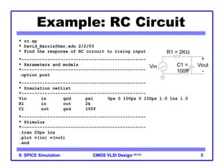
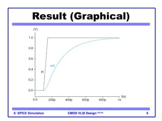
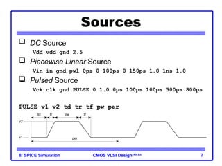
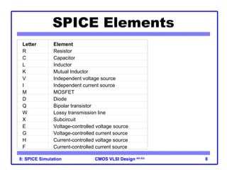
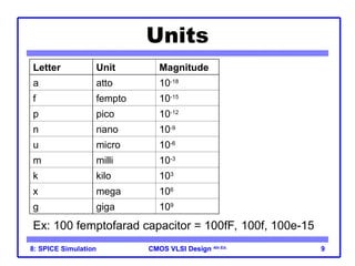
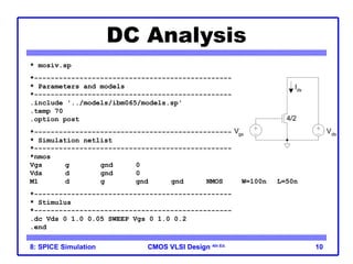
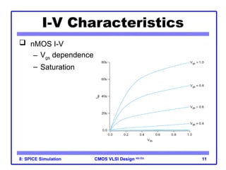
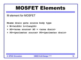
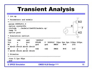
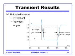
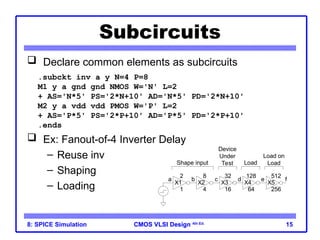
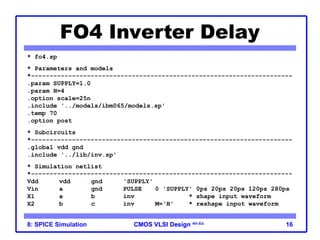
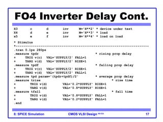
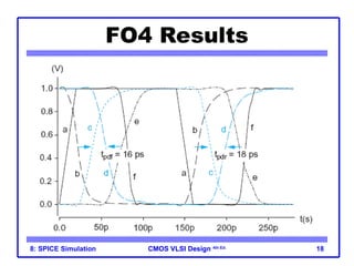
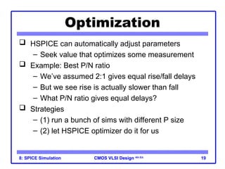
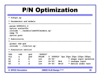
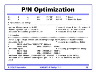
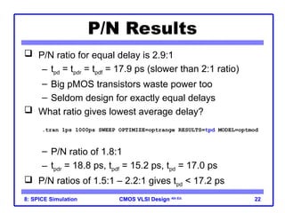
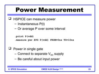
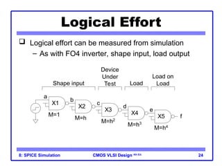
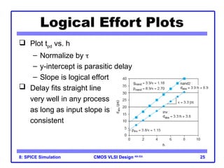
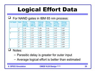
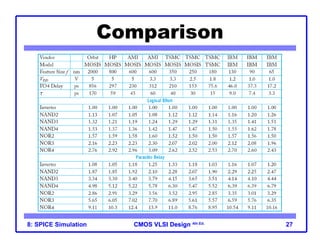
Lecture 8:
SPICE
Simulation
CMOS VLSI Design
CMOS VLSI Design 4th Ed.
8: SPICE Simulation 2
Outline
 Introduction to SPICE
 DC Analysis
 Transient Analysis
 Subcircuits
 Optimization
 Power Measurement
 Logical Effort Characterization
CMOS VLSI Design
CMOS VLSI Design 4th Ed.
8: SPICE Simulation 3
Introduction to SPICE
 Simulation Program with Integrated Circuit Emphasis
– Developed in 1970’s at Berkeley
– Many commercial versions are available
– HSPICE is a robust industry standard
• Has many enhancements that we will use
 Written in FORTRAN for punch-card machines
– Circuits elements are called cards
– Complete description is called a SPICE deck
CMOS VLSI Design
CMOS VLSI Design 4th Ed.
8: SPICE Simulation 4
Writing Spice Decks
 Writing a SPICE deck is like writing a good program
– Plan: sketch schematic on paper or in editor
• Modify existing decks whenever possible
– Code: strive for clarity
• Start with name, email, date, purpose
• Generously comment
– Test:
• Predict what results should be
• Compare with actual
• Garbage In, Garbage Out!
CMOS VLSI Design
CMOS VLSI Design 4th Ed.
8: SPICE Simulation 5
Example: RC Circuit
* rc.sp
* David_Harris@hmc.edu 2/2/03
* Find the response of RC circuit to rising input
*------------------------------------------------
* Parameters and models
*------------------------------------------------
.option post
*------------------------------------------------
* Simulation netlist
*------------------------------------------------
Vin in gnd pwl 0ps 0 100ps 0 150ps 1.0 1ns 1.0
R1 in out 2k
C1 out gnd 100f
*------------------------------------------------
* Stimulus
*------------------------------------------------
.tran 20ps 1ns
.plot v(in) v(out)
.end
R1 = 2K
C1 =
100fF
Vin
+
Vout
-
CMOS VLSI Design
CMOS VLSI Design 4th Ed.
8: SPICE Simulation 6
Result (Graphical)
CMOS VLSI Design
CMOS VLSI Design 4th Ed.
8: SPICE Simulation 7
Sources
 DC Source
Vdd vdd gnd 2.5
 Piecewise Linear Source
Vin in gnd pwl 0ps 0 100ps 0 150ps 1.0 1ns 1.0
 Pulsed Source
Vck clk gnd PULSE 0 1.0 0ps 100ps 100ps 300ps 800ps
PULSE v1 v2 td tr tf pw per
v1
v2
td tr tf
pw
per
CMOS VLSI Design
CMOS VLSI Design 4th Ed.
8: SPICE Simulation 8
SPICE Elements
Letter Element
R Resistor
C Capacitor
L Inductor
K Mutual Inductor
V Independent voltage source
I Independent current source
M MOSFET
D Diode
Q Bipolar transistor
W Lossy transmission line
X Subcircuit
E Voltage-controlled voltage source
G Voltage-controlled current source
H Current-controlled voltage source
F Current-controlled current source
CMOS VLSI Design
CMOS VLSI Design 4th Ed.
8: SPICE Simulation 9
Units
Letter Unit Magnitude
a atto 10-18
f fempto 10-15
p pico 10-12
n nano 10-9
u micro 10-6
m milli 10-3
k kilo 103
x mega 106
g giga 109
Ex: 100 femptofarad capacitor = 100fF, 100f, 100e-15
CMOS VLSI Design
CMOS VLSI Design 4th Ed.
8: SPICE Simulation 10
DC Analysis
* mosiv.sp
*------------------------------------------------
* Parameters and models
*------------------------------------------------
.include '../models/ibm065/models.sp'
.temp 70
.option post
*------------------------------------------------
* Simulation netlist
*------------------------------------------------
*nmos
Vgs g gnd 0
Vds d gnd 0
M1 d g gnd gnd NMOS W=100n L=50n
*------------------------------------------------
* Stimulus
*------------------------------------------------
.dc Vds 0 1.0 0.05 SWEEP Vgs 0 1.0 0.2
.end
Vgs
Vds
Ids
4/2
CMOS VLSI Design
CMOS VLSI Design 4th Ed.
8: SPICE Simulation 11
I-V Characteristics
 nMOS I-V
– Vgs dependence
– Saturation
CMOS VLSI Design
CMOS VLSI Design 4th Ed.
8: SPICE Simulation 12
MOSFET Elements
M element for MOSFET
Mname drain gate source body type
+ W=<width> L=<length>
+ AS=<area source> AD = <area drain>
+ PS=<perimeter source> PD=<perimeter drain>
CMOS VLSI Design
CMOS VLSI Design 4th Ed.
8: SPICE Simulation 13
Transient Analysis
* inv.sp
* Parameters and models
*------------------------------------------------
.param SUPPLY=1.0
.option scale=25n
.include '../models/ibm065/models.sp'
.temp 70
.option post
* Simulation netlist
*------------------------------------------------
Vdd vdd gnd 'SUPPLY'
Vin a gnd PULSE 0 'SUPPLY' 50ps 0ps 0ps 100ps 200ps
M1 y a gnd gnd NMOS W=4 L=2
+ AS=20 PS=18 AD=20 PD=18
M2 y a vdd vdd PMOS W=8 L=2
+ AS=40 PS=26 AD=40 PD=26
* Stimulus
*------------------------------------------------
.tran 0.1ps 80ps
.end
a
y
4/2
8/2
CMOS VLSI Design
CMOS VLSI Design 4th Ed.
8: SPICE Simulation 14
Transient Results
 Unloaded inverter
– Overshoot
– Very fast
edges
CMOS VLSI Design
CMOS VLSI Design 4th Ed.
8: SPICE Simulation 15
Subcircuits
 Declare common elements as subcircuits
 Ex: Fanout-of-4 Inverter Delay
– Reuse inv
– Shaping
– Loading
.subckt inv a y N=4 P=8
M1 y a gnd gnd NMOS W='N' L=2
+ AS='N*5' PS='2*N+10' AD='N*5' PD='2*N+10'
M2 y a vdd vdd PMOS W='P' L=2
+ AS='P*5' PS='2*P+10' AD='P*5' PD='2*P+10'
.ends
a b c d e
X1 X2 X3 X4
1
2
4
8
16
32
64
128
f
X5
256
512
Shape input
Device
Under
Test Load
Load on
Load
CMOS VLSI Design
CMOS VLSI Design 4th Ed.
8: SPICE Simulation 16
FO4 Inverter Delay
* fo4.sp
* Parameters and models
*----------------------------------------------------------------------
.param SUPPLY=1.0
.param H=4
.option scale=25n
.include '../models/ibm065/models.sp'
.temp 70
.option post
* Subcircuits
*----------------------------------------------------------------------
.global vdd gnd
.include '../lib/inv.sp'
* Simulation netlist
*----------------------------------------------------------------------
Vdd vdd gnd 'SUPPLY'
Vin a gnd PULSE 0 'SUPPLY' 0ps 20ps 20ps 120ps 280ps
X1 a b inv * shape input waveform
X2 b c inv M='H' * reshape input waveform
CMOS VLSI Design
CMOS VLSI Design 4th Ed.
8: SPICE Simulation 17
FO4 Inverter Delay Cont.
X3 c d inv M='H**2' * device under test
X4 d e inv M='H**3' * load
x5 e f inv M='H**4' * load on load
* Stimulus
*----------------------------------------------------------------------
.tran 0.1ps 280ps
.measure tpdr * rising prop delay
+ TRIG v(c) VAL='SUPPLY/2' FALL=1
+ TARG v(d) VAL='SUPPLY/2' RISE=1
.measure tpdf * falling prop delay
+ TRIG v(c) VAL='SUPPLY/2' RISE=1
+ TARG v(d) VAL='SUPPLY/2' FALL=1
.measure tpd param='(tpdr+tpdf)/2' * average prop delay
.measure trise * rise time
+ TRIG v(d) VAL='0.2*SUPPLY' RISE=1
+ TARG v(d) VAL='0.8*SUPPLY' RISE=1
.measure tfall * fall time
+ TRIG v(d) VAL='0.8*SUPPLY' FALL=1
+ TARG v(d) VAL='0.2*SUPPLY' FALL=1
.end
CMOS VLSI Design
CMOS VLSI Design 4th Ed.
8: SPICE Simulation 18
FO4 Results
CMOS VLSI Design
CMOS VLSI Design 4th Ed.
8: SPICE Simulation 19
Optimization
 HSPICE can automatically adjust parameters
– Seek value that optimizes some measurement
 Example: Best P/N ratio
– We’ve assumed 2:1 gives equal rise/fall delays
– But we see rise is actually slower than fall
– What P/N ratio gives equal delays?
 Strategies
– (1) run a bunch of sims with different P size
– (2) let HSPICE optimizer do it for us
CMOS VLSI Design
CMOS VLSI Design 4th Ed.
8: SPICE Simulation 20
P/N Optimization
* fo4opt.sp
* Parameters and models
*----------------------------------------------------------------------
.param SUPPLY=1.0
.option scale=25n
.include '../models/ibm065/models.sp'
.temp 70
.option post
* Subcircuits
*----------------------------------------------------------------------
.global vdd gnd
.include '../lib/inv.sp'
* Simulation netlist
*----------------------------------------------------------------------
Vdd vdd gnd 'SUPPLY'
Vin a gnd PULSE 0 'SUPPLY' 0ps 20ps 20ps 120ps 280ps
X1 a b inv P='P1' * shape input waveform
X2 b c inv P='P1' M=4 * reshape input
X3 c d inv P='P1' M=16 * device under test
CMOS VLSI Design
CMOS VLSI Design 4th Ed.
8: SPICE Simulation 21
P/N Optimization
X4 d e inv P='P1' M=64 * load
X5 e f inv P='P1' M=256 * load on load
* Optimization setup
*----------------------------------------------------------------------
.param P1=optrange(8,4,16) * search from 4 to 16, guess 8
.model optmod opt itropt=30 * maximum of 30 iterations
.measure bestratio param='P1/4' * compute best P/N ratio
* Stimulus
*----------------------------------------------------------------------
.tran 0.1ps 280ps SWEEP OPTIMIZE=optrange RESULTS=diff MODEL=optmod
.measure tpdr * rising propagation delay
+ TRIG v(c)VAL='SUPPLY/2' FALL=1
+ TARG v(d) VAL='SUPPLY/2' RISE=1
.measure tpdf * falling propagation delay
+ TRIG v(c) VAL='SUPPLY/2' RISE=1
+ TARG v(d) VAL='SUPPLY/2' FALL=1
.measure tpd param='(tpdr+tpdf)/2' goal=0 * average prop delay
.measure diff param='tpdr-tpdf' goal = 0 * diff between delays
.end
CMOS VLSI Design
CMOS VLSI Design 4th Ed.
8: SPICE Simulation 22
P/N Results
 P/N ratio for equal delay is 2.9:1
– tpd = tpdr = tpdf = 17.9 ps (slower than 2:1 ratio)
– Big pMOS transistors waste power too
– Seldom design for exactly equal delays
 What ratio gives lowest average delay?
.tran 1ps 1000ps SWEEP OPTIMIZE=optrange RESULTS=tpd MODEL=optmod
– P/N ratio of 1.8:1
– tpdr = 18.8 ps, tpdf = 15.2 ps, tpd = 17.0 ps
 P/N ratios of 1.5:1 – 2.2:1 gives tpd < 17.2 ps
CMOS VLSI Design
CMOS VLSI Design 4th Ed.
8: SPICE Simulation 23
Power Measurement
 HSPICE can measure power
– Instantaneous P(t)
– Or average P over some interval
.print P(vdd)
.measure pwr AVG P(vdd) FROM=0ns TO=10ns
 Power in single gate
– Connect to separate VDD supply
– Be careful about input power
CMOS VLSI Design
CMOS VLSI Design 4th Ed.
8: SPICE Simulation 24
Logical Effort
 Logical effort can be measured from simulation
– As with FO4 inverter, shape input, load output
X1
X2
X3
X4
X5
a
b
c
d
e
f
M=1
M=h
M=h2
M=h3
M=h4
Shape input
Device
Under
Test Load
Load on
Load
CMOS VLSI Design
CMOS VLSI Design 4th Ed.
8: SPICE Simulation 25
Logical Effort Plots
 Plot tpd vs. h
– Normalize by 
– y-intercept is parasitic delay
– Slope is logical effort
 Delay fits straight line
very well in any process
as long as input slope is
consistent
CMOS VLSI Design
CMOS VLSI Design 4th Ed.
8: SPICE Simulation 26
Logical Effort Data
 For NAND gates in IBM 65 nm process:
 Notes:
– Parasitic delay is greater for outer input
– Average logical effort is better than estimated
CMOS VLSI Design
CMOS VLSI Design 4th Ed.
8: SPICE Simulation 27
Comparison

Using p-Spice in VLSI design and Testing

  • 1.
  • 2.
    CMOS VLSI Design CMOSVLSI Design 4th Ed. 8: SPICE Simulation 2 Outline  Introduction to SPICE  DC Analysis  Transient Analysis  Subcircuits  Optimization  Power Measurement  Logical Effort Characterization
  • 3.
    CMOS VLSI Design CMOSVLSI Design 4th Ed. 8: SPICE Simulation 3 Introduction to SPICE  Simulation Program with Integrated Circuit Emphasis – Developed in 1970’s at Berkeley – Many commercial versions are available – HSPICE is a robust industry standard • Has many enhancements that we will use  Written in FORTRAN for punch-card machines – Circuits elements are called cards – Complete description is called a SPICE deck
  • 4.
    CMOS VLSI Design CMOSVLSI Design 4th Ed. 8: SPICE Simulation 4 Writing Spice Decks  Writing a SPICE deck is like writing a good program – Plan: sketch schematic on paper or in editor • Modify existing decks whenever possible – Code: strive for clarity • Start with name, email, date, purpose • Generously comment – Test: • Predict what results should be • Compare with actual • Garbage In, Garbage Out!
  • 5.
    CMOS VLSI Design CMOSVLSI Design 4th Ed. 8: SPICE Simulation 5 Example: RC Circuit * rc.sp * David_Harris@hmc.edu 2/2/03 * Find the response of RC circuit to rising input *------------------------------------------------ * Parameters and models *------------------------------------------------ .option post *------------------------------------------------ * Simulation netlist *------------------------------------------------ Vin in gnd pwl 0ps 0 100ps 0 150ps 1.0 1ns 1.0 R1 in out 2k C1 out gnd 100f *------------------------------------------------ * Stimulus *------------------------------------------------ .tran 20ps 1ns .plot v(in) v(out) .end R1 = 2K C1 = 100fF Vin + Vout -
  • 6.
    CMOS VLSI Design CMOSVLSI Design 4th Ed. 8: SPICE Simulation 6 Result (Graphical)
  • 7.
    CMOS VLSI Design CMOSVLSI Design 4th Ed. 8: SPICE Simulation 7 Sources  DC Source Vdd vdd gnd 2.5  Piecewise Linear Source Vin in gnd pwl 0ps 0 100ps 0 150ps 1.0 1ns 1.0  Pulsed Source Vck clk gnd PULSE 0 1.0 0ps 100ps 100ps 300ps 800ps PULSE v1 v2 td tr tf pw per v1 v2 td tr tf pw per
  • 8.
    CMOS VLSI Design CMOSVLSI Design 4th Ed. 8: SPICE Simulation 8 SPICE Elements Letter Element R Resistor C Capacitor L Inductor K Mutual Inductor V Independent voltage source I Independent current source M MOSFET D Diode Q Bipolar transistor W Lossy transmission line X Subcircuit E Voltage-controlled voltage source G Voltage-controlled current source H Current-controlled voltage source F Current-controlled current source
  • 9.
    CMOS VLSI Design CMOSVLSI Design 4th Ed. 8: SPICE Simulation 9 Units Letter Unit Magnitude a atto 10-18 f fempto 10-15 p pico 10-12 n nano 10-9 u micro 10-6 m milli 10-3 k kilo 103 x mega 106 g giga 109 Ex: 100 femptofarad capacitor = 100fF, 100f, 100e-15
  • 10.
    CMOS VLSI Design CMOSVLSI Design 4th Ed. 8: SPICE Simulation 10 DC Analysis * mosiv.sp *------------------------------------------------ * Parameters and models *------------------------------------------------ .include '../models/ibm065/models.sp' .temp 70 .option post *------------------------------------------------ * Simulation netlist *------------------------------------------------ *nmos Vgs g gnd 0 Vds d gnd 0 M1 d g gnd gnd NMOS W=100n L=50n *------------------------------------------------ * Stimulus *------------------------------------------------ .dc Vds 0 1.0 0.05 SWEEP Vgs 0 1.0 0.2 .end Vgs Vds Ids 4/2
  • 11.
    CMOS VLSI Design CMOSVLSI Design 4th Ed. 8: SPICE Simulation 11 I-V Characteristics  nMOS I-V – Vgs dependence – Saturation
  • 12.
    CMOS VLSI Design CMOSVLSI Design 4th Ed. 8: SPICE Simulation 12 MOSFET Elements M element for MOSFET Mname drain gate source body type + W=<width> L=<length> + AS=<area source> AD = <area drain> + PS=<perimeter source> PD=<perimeter drain>
  • 13.
    CMOS VLSI Design CMOSVLSI Design 4th Ed. 8: SPICE Simulation 13 Transient Analysis * inv.sp * Parameters and models *------------------------------------------------ .param SUPPLY=1.0 .option scale=25n .include '../models/ibm065/models.sp' .temp 70 .option post * Simulation netlist *------------------------------------------------ Vdd vdd gnd 'SUPPLY' Vin a gnd PULSE 0 'SUPPLY' 50ps 0ps 0ps 100ps 200ps M1 y a gnd gnd NMOS W=4 L=2 + AS=20 PS=18 AD=20 PD=18 M2 y a vdd vdd PMOS W=8 L=2 + AS=40 PS=26 AD=40 PD=26 * Stimulus *------------------------------------------------ .tran 0.1ps 80ps .end a y 4/2 8/2
  • 14.
    CMOS VLSI Design CMOSVLSI Design 4th Ed. 8: SPICE Simulation 14 Transient Results  Unloaded inverter – Overshoot – Very fast edges
  • 15.
    CMOS VLSI Design CMOSVLSI Design 4th Ed. 8: SPICE Simulation 15 Subcircuits  Declare common elements as subcircuits  Ex: Fanout-of-4 Inverter Delay – Reuse inv – Shaping – Loading .subckt inv a y N=4 P=8 M1 y a gnd gnd NMOS W='N' L=2 + AS='N*5' PS='2*N+10' AD='N*5' PD='2*N+10' M2 y a vdd vdd PMOS W='P' L=2 + AS='P*5' PS='2*P+10' AD='P*5' PD='2*P+10' .ends a b c d e X1 X2 X3 X4 1 2 4 8 16 32 64 128 f X5 256 512 Shape input Device Under Test Load Load on Load
  • 16.
    CMOS VLSI Design CMOSVLSI Design 4th Ed. 8: SPICE Simulation 16 FO4 Inverter Delay * fo4.sp * Parameters and models *---------------------------------------------------------------------- .param SUPPLY=1.0 .param H=4 .option scale=25n .include '../models/ibm065/models.sp' .temp 70 .option post * Subcircuits *---------------------------------------------------------------------- .global vdd gnd .include '../lib/inv.sp' * Simulation netlist *---------------------------------------------------------------------- Vdd vdd gnd 'SUPPLY' Vin a gnd PULSE 0 'SUPPLY' 0ps 20ps 20ps 120ps 280ps X1 a b inv * shape input waveform X2 b c inv M='H' * reshape input waveform
  • 17.
    CMOS VLSI Design CMOSVLSI Design 4th Ed. 8: SPICE Simulation 17 FO4 Inverter Delay Cont. X3 c d inv M='H**2' * device under test X4 d e inv M='H**3' * load x5 e f inv M='H**4' * load on load * Stimulus *---------------------------------------------------------------------- .tran 0.1ps 280ps .measure tpdr * rising prop delay + TRIG v(c) VAL='SUPPLY/2' FALL=1 + TARG v(d) VAL='SUPPLY/2' RISE=1 .measure tpdf * falling prop delay + TRIG v(c) VAL='SUPPLY/2' RISE=1 + TARG v(d) VAL='SUPPLY/2' FALL=1 .measure tpd param='(tpdr+tpdf)/2' * average prop delay .measure trise * rise time + TRIG v(d) VAL='0.2*SUPPLY' RISE=1 + TARG v(d) VAL='0.8*SUPPLY' RISE=1 .measure tfall * fall time + TRIG v(d) VAL='0.8*SUPPLY' FALL=1 + TARG v(d) VAL='0.2*SUPPLY' FALL=1 .end
  • 18.
    CMOS VLSI Design CMOSVLSI Design 4th Ed. 8: SPICE Simulation 18 FO4 Results
  • 19.
    CMOS VLSI Design CMOSVLSI Design 4th Ed. 8: SPICE Simulation 19 Optimization  HSPICE can automatically adjust parameters – Seek value that optimizes some measurement  Example: Best P/N ratio – We’ve assumed 2:1 gives equal rise/fall delays – But we see rise is actually slower than fall – What P/N ratio gives equal delays?  Strategies – (1) run a bunch of sims with different P size – (2) let HSPICE optimizer do it for us
  • 20.
    CMOS VLSI Design CMOSVLSI Design 4th Ed. 8: SPICE Simulation 20 P/N Optimization * fo4opt.sp * Parameters and models *---------------------------------------------------------------------- .param SUPPLY=1.0 .option scale=25n .include '../models/ibm065/models.sp' .temp 70 .option post * Subcircuits *---------------------------------------------------------------------- .global vdd gnd .include '../lib/inv.sp' * Simulation netlist *---------------------------------------------------------------------- Vdd vdd gnd 'SUPPLY' Vin a gnd PULSE 0 'SUPPLY' 0ps 20ps 20ps 120ps 280ps X1 a b inv P='P1' * shape input waveform X2 b c inv P='P1' M=4 * reshape input X3 c d inv P='P1' M=16 * device under test
  • 21.
    CMOS VLSI Design CMOSVLSI Design 4th Ed. 8: SPICE Simulation 21 P/N Optimization X4 d e inv P='P1' M=64 * load X5 e f inv P='P1' M=256 * load on load * Optimization setup *---------------------------------------------------------------------- .param P1=optrange(8,4,16) * search from 4 to 16, guess 8 .model optmod opt itropt=30 * maximum of 30 iterations .measure bestratio param='P1/4' * compute best P/N ratio * Stimulus *---------------------------------------------------------------------- .tran 0.1ps 280ps SWEEP OPTIMIZE=optrange RESULTS=diff MODEL=optmod .measure tpdr * rising propagation delay + TRIG v(c)VAL='SUPPLY/2' FALL=1 + TARG v(d) VAL='SUPPLY/2' RISE=1 .measure tpdf * falling propagation delay + TRIG v(c) VAL='SUPPLY/2' RISE=1 + TARG v(d) VAL='SUPPLY/2' FALL=1 .measure tpd param='(tpdr+tpdf)/2' goal=0 * average prop delay .measure diff param='tpdr-tpdf' goal = 0 * diff between delays .end
  • 22.
    CMOS VLSI Design CMOSVLSI Design 4th Ed. 8: SPICE Simulation 22 P/N Results  P/N ratio for equal delay is 2.9:1 – tpd = tpdr = tpdf = 17.9 ps (slower than 2:1 ratio) – Big pMOS transistors waste power too – Seldom design for exactly equal delays  What ratio gives lowest average delay? .tran 1ps 1000ps SWEEP OPTIMIZE=optrange RESULTS=tpd MODEL=optmod – P/N ratio of 1.8:1 – tpdr = 18.8 ps, tpdf = 15.2 ps, tpd = 17.0 ps  P/N ratios of 1.5:1 – 2.2:1 gives tpd < 17.2 ps
  • 23.
    CMOS VLSI Design CMOSVLSI Design 4th Ed. 8: SPICE Simulation 23 Power Measurement  HSPICE can measure power – Instantaneous P(t) – Or average P over some interval .print P(vdd) .measure pwr AVG P(vdd) FROM=0ns TO=10ns  Power in single gate – Connect to separate VDD supply – Be careful about input power
  • 24.
    CMOS VLSI Design CMOSVLSI Design 4th Ed. 8: SPICE Simulation 24 Logical Effort  Logical effort can be measured from simulation – As with FO4 inverter, shape input, load output X1 X2 X3 X4 X5 a b c d e f M=1 M=h M=h2 M=h3 M=h4 Shape input Device Under Test Load Load on Load
  • 25.
    CMOS VLSI Design CMOSVLSI Design 4th Ed. 8: SPICE Simulation 25 Logical Effort Plots  Plot tpd vs. h – Normalize by  – y-intercept is parasitic delay – Slope is logical effort  Delay fits straight line very well in any process as long as input slope is consistent
  • 26.
    CMOS VLSI Design CMOSVLSI Design 4th Ed. 8: SPICE Simulation 26 Logical Effort Data  For NAND gates in IBM 65 nm process:  Notes: – Parasitic delay is greater for outer input – Average logical effort is better than estimated
  • 27.
    CMOS VLSI Design CMOSVLSI Design 4th Ed. 8: SPICE Simulation 27 Comparison