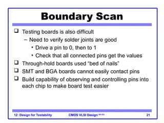
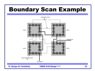
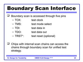
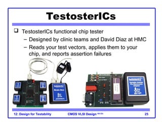
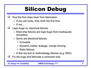
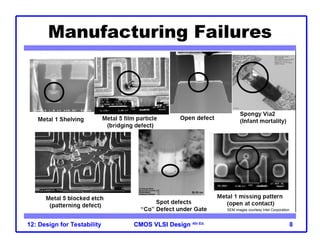
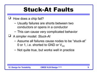
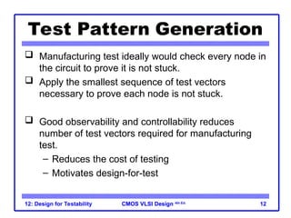
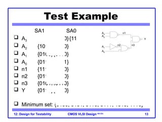
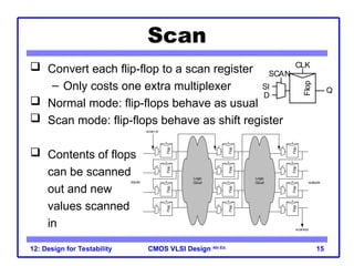
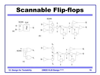
Lecture 12:
Design for
Testability
CMOS VLSI Design
CMOS VLSI Design 4th Ed.
12: Design for Testability 2
Outline
 Testing
– Logic Verification
– Silicon Debug
– Manufacturing Test
 Fault Models
 Observability and Controllability
 Design for Test
– Scan
– BIST
 Boundary Scan
CMOS VLSI Design
CMOS VLSI Design 4th Ed.
12: Design for Testability 3
Testing
 Testing is one of the most expensive parts of chips
– Logic verification accounts for > 50% of design
effort for many chips
– Debug time after fabrication has enormous
opportunity cost
– Shipping defective parts can sink a company
 Example: Intel FDIV bug (1994)
– Logic error not caught until > 1M units shipped
– Recall cost $450M (!!!)
CMOS VLSI Design
CMOS VLSI Design 4th Ed.
12: Design for Testability 4
Logic Verification
 Does the chip simulate correctly?
– Usually done at HDL level
– Verification engineers write test bench for HDL
• Can’t test all cases
• Look for corner cases
• Try to break logic design
 Ex: 32-bit adder
– Test all combinations of corner cases as inputs:
• 0, 1, 2, 231
-1, -1, -231
, a few random numbers
 Good tests require ingenuity
CMOS VLSI Design
CMOS VLSI Design 4th Ed.
12: Design for Testability 5
Silicon Debug
 Test the first chips back from fabrication
– If you are lucky, they work the first time
– If not…
 Logic bugs vs. electrical failures
– Most chip failures are logic bugs from inadequate
simulation
– Some are electrical failures
• Crosstalk
• Dynamic nodes: leakage, charge sharing
• Ratio failures
– A few are tool or methodology failures (e.g. DRC)
 Fix the bugs and fabricate a corrected chip
CMOS VLSI Design
CMOS VLSI Design 4th Ed.
12: Design for Testability 6
Shmoo Plots
 How to diagnose failures?
– Hard to access chips
• Picoprobes
• Electron beam
• Laser voltage probing
• Built-in self-test
 Shmoo plots
– Vary voltage, frequency
– Look for cause of
electrical failures
CMOS VLSI Design
CMOS VLSI Design 4th Ed.
12: Design for Testability 7
Manufacturing Test
 A speck of dust on a wafer is sufficient to kill chip
 Yield of any chip is < 100%
– Must test chips after manufacturing before
delivery to customers to only ship good parts
 Manufacturing testers are
very expensive
– Minimize time on tester
– Careful selection of
test vectors
CMOS VLSI Design
CMOS VLSI Design 4th Ed.
12: Design for Testability 8
Manufacturing Failures
SEM images courtesy Intel Corporation
CMOS VLSI Design
CMOS VLSI Design 4th Ed.
12: Design for Testability 9
Stuck-At Faults
 How does a chip fail?
– Usually failures are shorts between two
conductors or opens in a conductor
– This can cause very complicated behavior
 A simpler model: Stuck-At
– Assume all failures cause nodes to be “stuck-at”
0 or 1, i.e. shorted to GND or VDD
– Not quite true, but works well in practice
CMOS VLSI Design
CMOS VLSI Design 4th Ed.
12: Design for Testability 10
Examples
CMOS VLSI Design
CMOS VLSI Design 4th Ed.
12: Design for Testability 11
Observability & Controllability
 Observability: ease of observing a node by watching
external output pins of the chip
 Controllability: ease of forcing a node to 0 or 1 by
driving input pins of the chip
 Combinational logic is usually easy to observe and
control
 Finite state machines can be very difficult, requiring
many cycles to enter desired state
– Especially if state transition diagram is not known
to the test engineer
CMOS VLSI Design
CMOS VLSI Design 4th Ed.
12: Design for Testability 12
Test Pattern Generation
 Manufacturing test ideally would check every node in
the circuit to prove it is not stuck.
 Apply the smallest sequence of test vectors
necessary to prove each node is not stuck.
 Good observability and controllability reduces
number of test vectors required for manufacturing
test.
– Reduces the cost of testing
– Motivates design-for-test
CMOS VLSI Design
CMOS VLSI Design 4th Ed.
12: Design for Testability 13
Test Example
SA1 SA0
 A3 {0110}{1110}
 A2 {1010}{1110}
 A1 {0100}{0110}
 A0 {0110}{0111}
 n1 {1110}{0110}
 n2 {0110}{0100}
 n3 {0101}{0110}
 Y {0110}{1110}
 Minimum set: {0100, 0101, 0110, 0111, 1010, 1110}
A3
A2
A1
A0
Y
n1
n2 n3
CMOS VLSI Design
CMOS VLSI Design 4th Ed.
12: Design for Testability 14
Design for Test
 Design the chip to increase observability and
controllability
 If each register could be observed and controlled,
test problem reduces to testing combinational logic
between registers.
 Better yet, logic blocks could enter test mode where
they generate test patterns and report the results
automatically.
CMOS VLSI Design
CMOS VLSI Design 4th Ed.
12: Design for Testability 15
Scan
 Convert each flip-flop to a scan register
– Only costs one extra multiplexer
 Normal mode: flip-flops behave as usual
 Scan mode: flip-flops behave as shift register
 Contents of flops
can be scanned
out and new
values scanned
in
Flop
Q
D
CLK
SI
SCAN
scanout
scan-in
inputs outputs
Flop
Flop
Flop
Flop
Flop
Flop
Flop
Flop
Flop
Flop
Flop
Flop
Logic
Cloud
Logic
Cloud
CMOS VLSI Design
CMOS VLSI Design 4th Ed.
12: Design for Testability 16
Scannable Flip-flops
0
1
Flop
CLK
D
SI
SCAN
Q
D




X
Q
Q




(a)
(b)
SCAN
SI
D


X
Q
Q




SI
s
s
(c)

d
d
d
s
SCAN
CMOS VLSI Design
CMOS VLSI Design 4th Ed.
12: Design for Testability 17
ATPG
 Test pattern generation is tedious
 Automatic Test Pattern Generation (ATPG) tools
produce a good set of vectors for each block of
combinational logic
 Scan chains are used to control and observe the
blocks
 Complete coverage requires a large number of
vectors, raising the cost of test
 Most products settle for covering 90+% of potential
stuck-at faults
CMOS VLSI Design
CMOS VLSI Design 4th Ed.
12: Design for Testability 18
Built-in Self-test
 Built-in self-test lets blocks test themselves
– Generate pseudo-random inputs to comb. logic
– Combine outputs into a syndrome
– With high probability, block is fault-free if it
produces the expected syndrome
CMOS VLSI Design
CMOS VLSI Design 4th Ed.
12: Design for Testability 19
PRSG
 Linear Feedback Shift Register
– Shift register with input taken from XOR of state
– Pseudo-Random Sequence Generator
Flop
Flop
Flop
Q[0] Q[1] Q[2]
CLK
D D D
Step Y
0 111
1 110
2 101
3 010
4 100
5 001
6 011
7 111 (repeats)
Flops reset to 111
Y
CMOS VLSI Design
CMOS VLSI Design 4th Ed.
12: Design for Testability 20
BILBO
 Built-in Logic Block Observer
– Combine scan with PRSG & signature analysis
MODE C[1] C[0]
Scan 0 0
Test 0 1
Reset 1 0
Normal 1 1
Flop
Flop
Flop
1
0
D[0] D[1] D[2]
Q[0]
Q[1]
Q[2] / SO
SI
C[1]
C[0]
PRSG
Logic
Cloud
Signature
Analyzer
CMOS VLSI Design
CMOS VLSI Design 4th Ed.
12: Design for Testability 21
Boundary Scan
 Testing boards is also difficult
– Need to verify solder joints are good
• Drive a pin to 0, then to 1
• Check that all connected pins get the values
 Through-hold boards used “bed of nails”
 SMT and BGA boards cannot easily contact pins
 Build capability of observing and controlling pins into
each chip to make board test easier
CMOS VLSI Design
CMOS VLSI Design 4th Ed.
12: Design for Testability 22
Boundary Scan Example
SerialData In
SerialData Out
PackageInterconnect
IOpad andBoundaryScan
Cell
CHIP A
CHIP B CHIP C
CHIP D
CMOS VLSI Design
CMOS VLSI Design 4th Ed.
12: Design for Testability 23
Boundary Scan Interface
 Boundary scan is accessed through five pins
– TCK: test clock
– TMS: test mode select
– TDI: test data in
– TDO: test data out
– TRST*: test reset (optional)
 Chips with internal scan chains can access the
chains through boundary scan for unified test
strategy.
CMOS VLSI Design
CMOS VLSI Design 4th Ed.
12: Design for Testability 24
Testing Your Class Project
 Presilicon Verification
– Test vectors: corner cases and random vectors
– HDL simulation of schematics for functionality
– Use 2-phase clocking to avoid races
– Use static CMOS gates to avoid electrical failures
– Use LVS to ensure layout matches schematic
– Don’t worry about timing
 Postsilicon Verification
– Run your test vectors on the fabricated chip
– Use a functional chip tester
– Potentially use breadboard or PCB for full system
CMOS VLSI Design
CMOS VLSI Design 4th Ed.
12: Design for Testability 25
TestosterICs
 TestosterICs functional chip tester
– Designed by clinic teams and David Diaz at HMC
– Reads your test vectors, applies them to your
chip, and reports assertion failures
CMOS VLSI Design
CMOS VLSI Design 4th Ed.
12: Design for Testability 26
Summary
 Think about testing from the beginning
– Simulate as you go
– Plan for test after fabrication
 “If you don’t test it, it won’t work! (Guaranteed)”

Test generation in VLSI design and Testing

  • 1.
  • 2.
    CMOS VLSI Design CMOSVLSI Design 4th Ed. 12: Design for Testability 2 Outline  Testing – Logic Verification – Silicon Debug – Manufacturing Test  Fault Models  Observability and Controllability  Design for Test – Scan – BIST  Boundary Scan
  • 3.
    CMOS VLSI Design CMOSVLSI Design 4th Ed. 12: Design for Testability 3 Testing  Testing is one of the most expensive parts of chips – Logic verification accounts for > 50% of design effort for many chips – Debug time after fabrication has enormous opportunity cost – Shipping defective parts can sink a company  Example: Intel FDIV bug (1994) – Logic error not caught until > 1M units shipped – Recall cost $450M (!!!)
  • 4.
    CMOS VLSI Design CMOSVLSI Design 4th Ed. 12: Design for Testability 4 Logic Verification  Does the chip simulate correctly? – Usually done at HDL level – Verification engineers write test bench for HDL • Can’t test all cases • Look for corner cases • Try to break logic design  Ex: 32-bit adder – Test all combinations of corner cases as inputs: • 0, 1, 2, 231 -1, -1, -231 , a few random numbers  Good tests require ingenuity
  • 5.
    CMOS VLSI Design CMOSVLSI Design 4th Ed. 12: Design for Testability 5 Silicon Debug  Test the first chips back from fabrication – If you are lucky, they work the first time – If not…  Logic bugs vs. electrical failures – Most chip failures are logic bugs from inadequate simulation – Some are electrical failures • Crosstalk • Dynamic nodes: leakage, charge sharing • Ratio failures – A few are tool or methodology failures (e.g. DRC)  Fix the bugs and fabricate a corrected chip
  • 6.
    CMOS VLSI Design CMOSVLSI Design 4th Ed. 12: Design for Testability 6 Shmoo Plots  How to diagnose failures? – Hard to access chips • Picoprobes • Electron beam • Laser voltage probing • Built-in self-test  Shmoo plots – Vary voltage, frequency – Look for cause of electrical failures
  • 7.
    CMOS VLSI Design CMOSVLSI Design 4th Ed. 12: Design for Testability 7 Manufacturing Test  A speck of dust on a wafer is sufficient to kill chip  Yield of any chip is < 100% – Must test chips after manufacturing before delivery to customers to only ship good parts  Manufacturing testers are very expensive – Minimize time on tester – Careful selection of test vectors
  • 8.
    CMOS VLSI Design CMOSVLSI Design 4th Ed. 12: Design for Testability 8 Manufacturing Failures SEM images courtesy Intel Corporation
  • 9.
    CMOS VLSI Design CMOSVLSI Design 4th Ed. 12: Design for Testability 9 Stuck-At Faults  How does a chip fail? – Usually failures are shorts between two conductors or opens in a conductor – This can cause very complicated behavior  A simpler model: Stuck-At – Assume all failures cause nodes to be “stuck-at” 0 or 1, i.e. shorted to GND or VDD – Not quite true, but works well in practice
  • 10.
    CMOS VLSI Design CMOSVLSI Design 4th Ed. 12: Design for Testability 10 Examples
  • 11.
    CMOS VLSI Design CMOSVLSI Design 4th Ed. 12: Design for Testability 11 Observability & Controllability  Observability: ease of observing a node by watching external output pins of the chip  Controllability: ease of forcing a node to 0 or 1 by driving input pins of the chip  Combinational logic is usually easy to observe and control  Finite state machines can be very difficult, requiring many cycles to enter desired state – Especially if state transition diagram is not known to the test engineer
  • 12.
    CMOS VLSI Design CMOSVLSI Design 4th Ed. 12: Design for Testability 12 Test Pattern Generation  Manufacturing test ideally would check every node in the circuit to prove it is not stuck.  Apply the smallest sequence of test vectors necessary to prove each node is not stuck.  Good observability and controllability reduces number of test vectors required for manufacturing test. – Reduces the cost of testing – Motivates design-for-test
  • 13.
    CMOS VLSI Design CMOSVLSI Design 4th Ed. 12: Design for Testability 13 Test Example SA1 SA0  A3 {0110}{1110}  A2 {1010}{1110}  A1 {0100}{0110}  A0 {0110}{0111}  n1 {1110}{0110}  n2 {0110}{0100}  n3 {0101}{0110}  Y {0110}{1110}  Minimum set: {0100, 0101, 0110, 0111, 1010, 1110} A3 A2 A1 A0 Y n1 n2 n3
  • 14.
    CMOS VLSI Design CMOSVLSI Design 4th Ed. 12: Design for Testability 14 Design for Test  Design the chip to increase observability and controllability  If each register could be observed and controlled, test problem reduces to testing combinational logic between registers.  Better yet, logic blocks could enter test mode where they generate test patterns and report the results automatically.
  • 15.
    CMOS VLSI Design CMOSVLSI Design 4th Ed. 12: Design for Testability 15 Scan  Convert each flip-flop to a scan register – Only costs one extra multiplexer  Normal mode: flip-flops behave as usual  Scan mode: flip-flops behave as shift register  Contents of flops can be scanned out and new values scanned in Flop Q D CLK SI SCAN scanout scan-in inputs outputs Flop Flop Flop Flop Flop Flop Flop Flop Flop Flop Flop Flop Logic Cloud Logic Cloud
  • 16.
    CMOS VLSI Design CMOSVLSI Design 4th Ed. 12: Design for Testability 16 Scannable Flip-flops 0 1 Flop CLK D SI SCAN Q D     X Q Q     (a) (b) SCAN SI D   X Q Q     SI s s (c)  d d d s SCAN
  • 17.
    CMOS VLSI Design CMOSVLSI Design 4th Ed. 12: Design for Testability 17 ATPG  Test pattern generation is tedious  Automatic Test Pattern Generation (ATPG) tools produce a good set of vectors for each block of combinational logic  Scan chains are used to control and observe the blocks  Complete coverage requires a large number of vectors, raising the cost of test  Most products settle for covering 90+% of potential stuck-at faults
  • 18.
    CMOS VLSI Design CMOSVLSI Design 4th Ed. 12: Design for Testability 18 Built-in Self-test  Built-in self-test lets blocks test themselves – Generate pseudo-random inputs to comb. logic – Combine outputs into a syndrome – With high probability, block is fault-free if it produces the expected syndrome
  • 19.
    CMOS VLSI Design CMOSVLSI Design 4th Ed. 12: Design for Testability 19 PRSG  Linear Feedback Shift Register – Shift register with input taken from XOR of state – Pseudo-Random Sequence Generator Flop Flop Flop Q[0] Q[1] Q[2] CLK D D D Step Y 0 111 1 110 2 101 3 010 4 100 5 001 6 011 7 111 (repeats) Flops reset to 111 Y
  • 20.
    CMOS VLSI Design CMOSVLSI Design 4th Ed. 12: Design for Testability 20 BILBO  Built-in Logic Block Observer – Combine scan with PRSG & signature analysis MODE C[1] C[0] Scan 0 0 Test 0 1 Reset 1 0 Normal 1 1 Flop Flop Flop 1 0 D[0] D[1] D[2] Q[0] Q[1] Q[2] / SO SI C[1] C[0] PRSG Logic Cloud Signature Analyzer
  • 21.
    CMOS VLSI Design CMOSVLSI Design 4th Ed. 12: Design for Testability 21 Boundary Scan  Testing boards is also difficult – Need to verify solder joints are good • Drive a pin to 0, then to 1 • Check that all connected pins get the values  Through-hold boards used “bed of nails”  SMT and BGA boards cannot easily contact pins  Build capability of observing and controlling pins into each chip to make board test easier
  • 22.
    CMOS VLSI Design CMOSVLSI Design 4th Ed. 12: Design for Testability 22 Boundary Scan Example SerialData In SerialData Out PackageInterconnect IOpad andBoundaryScan Cell CHIP A CHIP B CHIP C CHIP D
  • 23.
    CMOS VLSI Design CMOSVLSI Design 4th Ed. 12: Design for Testability 23 Boundary Scan Interface  Boundary scan is accessed through five pins – TCK: test clock – TMS: test mode select – TDI: test data in – TDO: test data out – TRST*: test reset (optional)  Chips with internal scan chains can access the chains through boundary scan for unified test strategy.
  • 24.
    CMOS VLSI Design CMOSVLSI Design 4th Ed. 12: Design for Testability 24 Testing Your Class Project  Presilicon Verification – Test vectors: corner cases and random vectors – HDL simulation of schematics for functionality – Use 2-phase clocking to avoid races – Use static CMOS gates to avoid electrical failures – Use LVS to ensure layout matches schematic – Don’t worry about timing  Postsilicon Verification – Run your test vectors on the fabricated chip – Use a functional chip tester – Potentially use breadboard or PCB for full system
  • 25.
    CMOS VLSI Design CMOSVLSI Design 4th Ed. 12: Design for Testability 25 TestosterICs  TestosterICs functional chip tester – Designed by clinic teams and David Diaz at HMC – Reads your test vectors, applies them to your chip, and reports assertion failures
  • 26.
    CMOS VLSI Design CMOSVLSI Design 4th Ed. 12: Design for Testability 26 Summary  Think about testing from the beginning – Simulate as you go – Plan for test after fabrication  “If you don’t test it, it won’t work! (Guaranteed)”