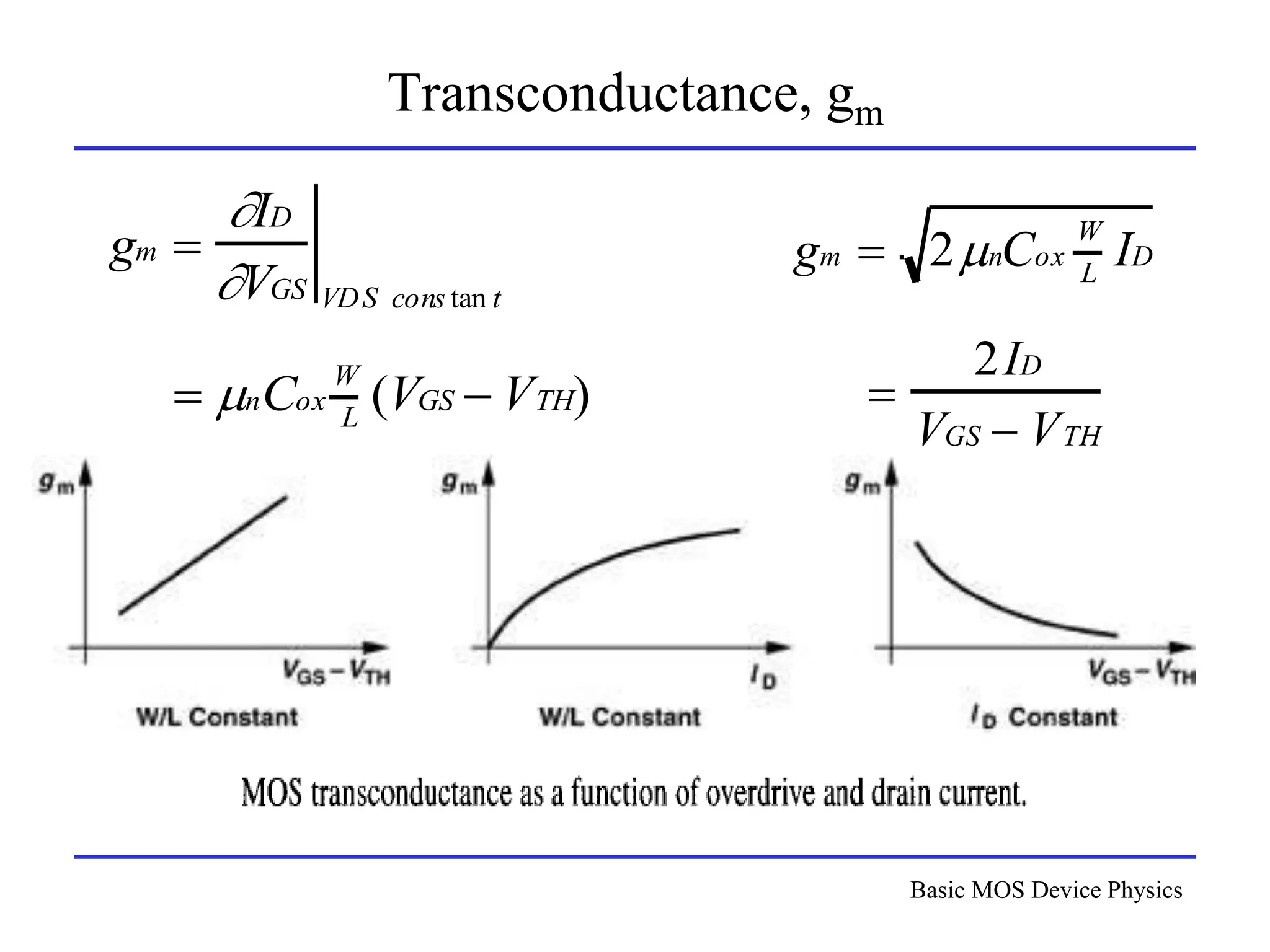
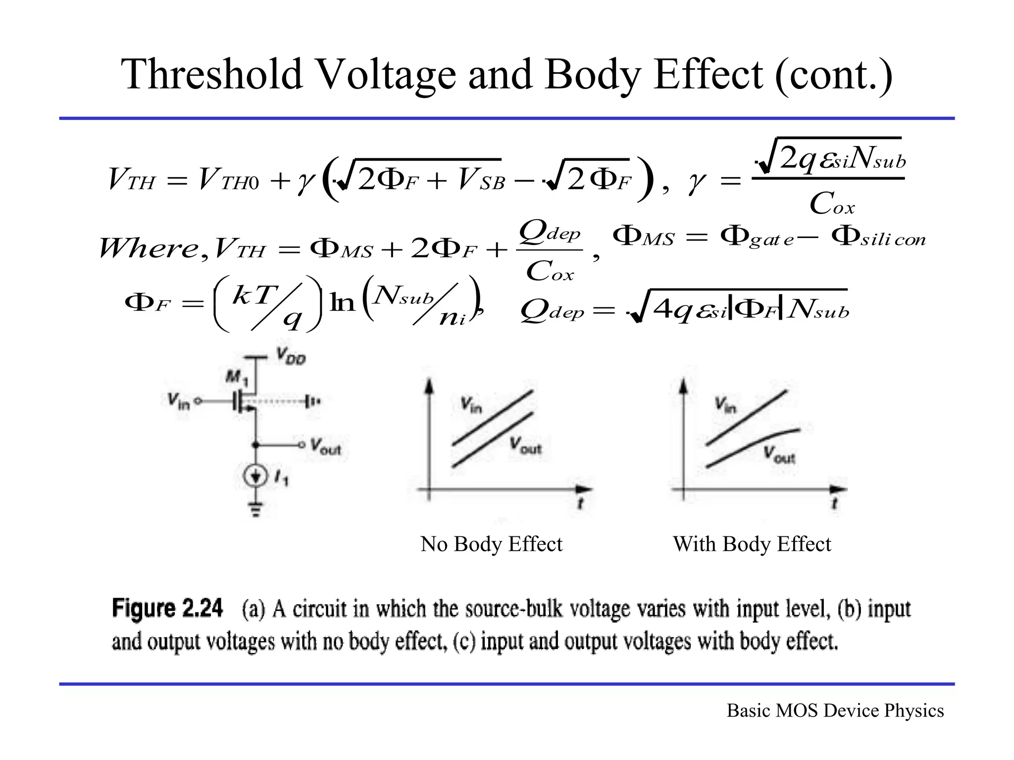
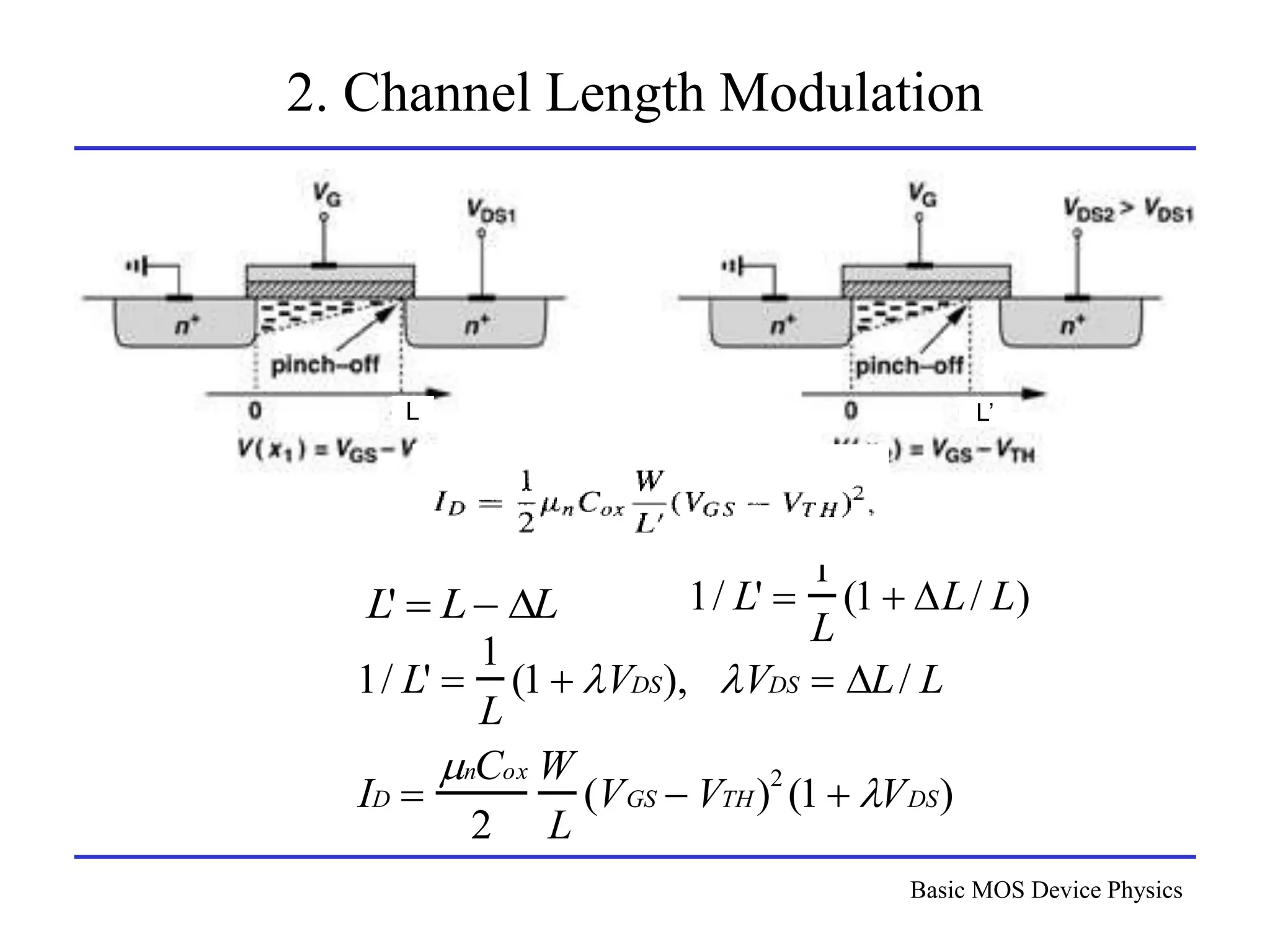
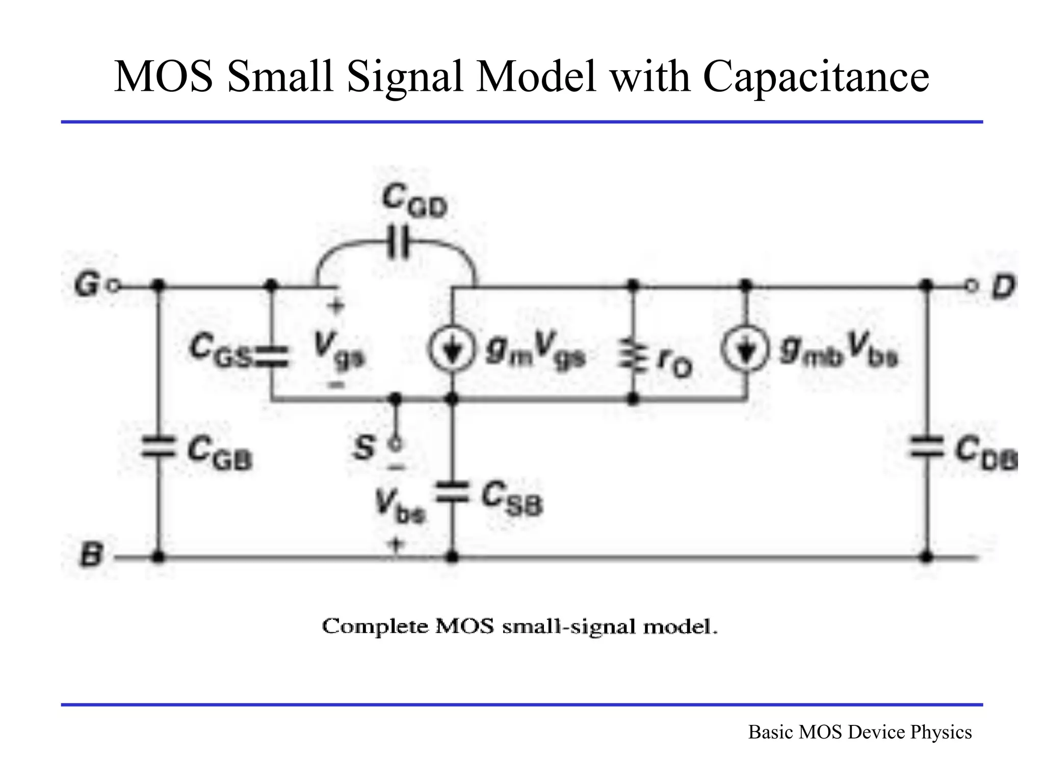
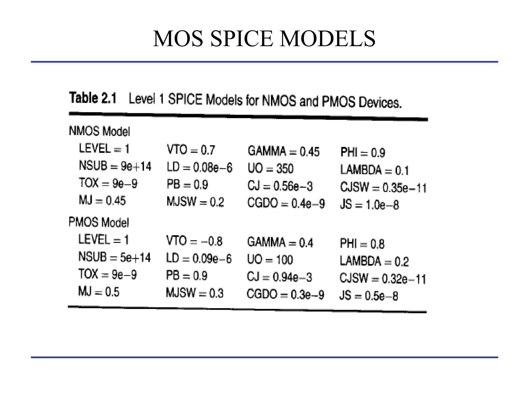
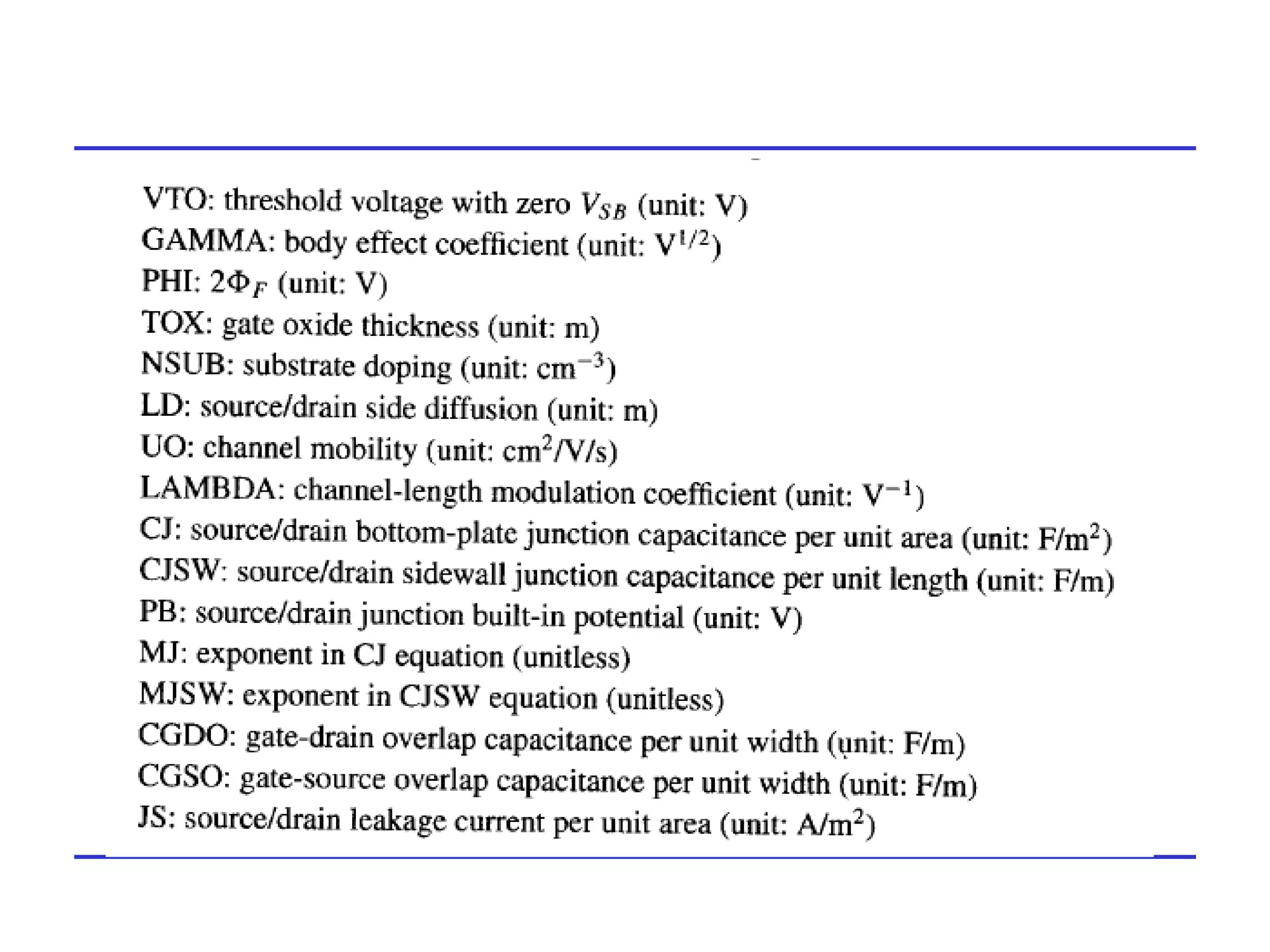
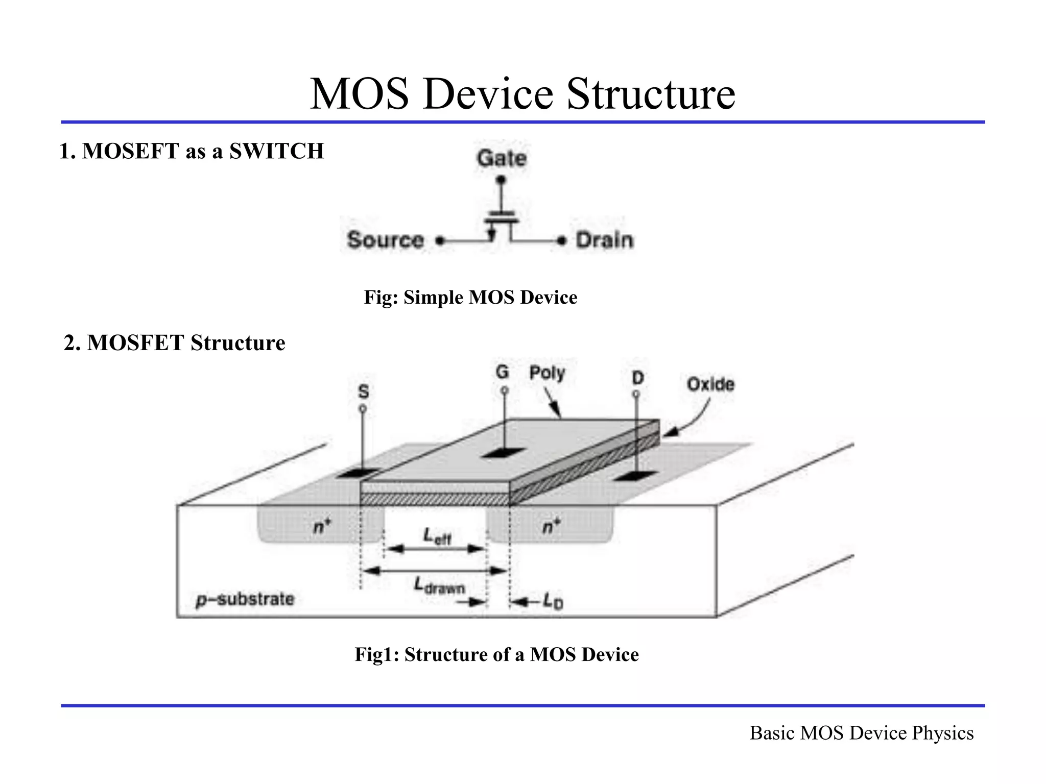
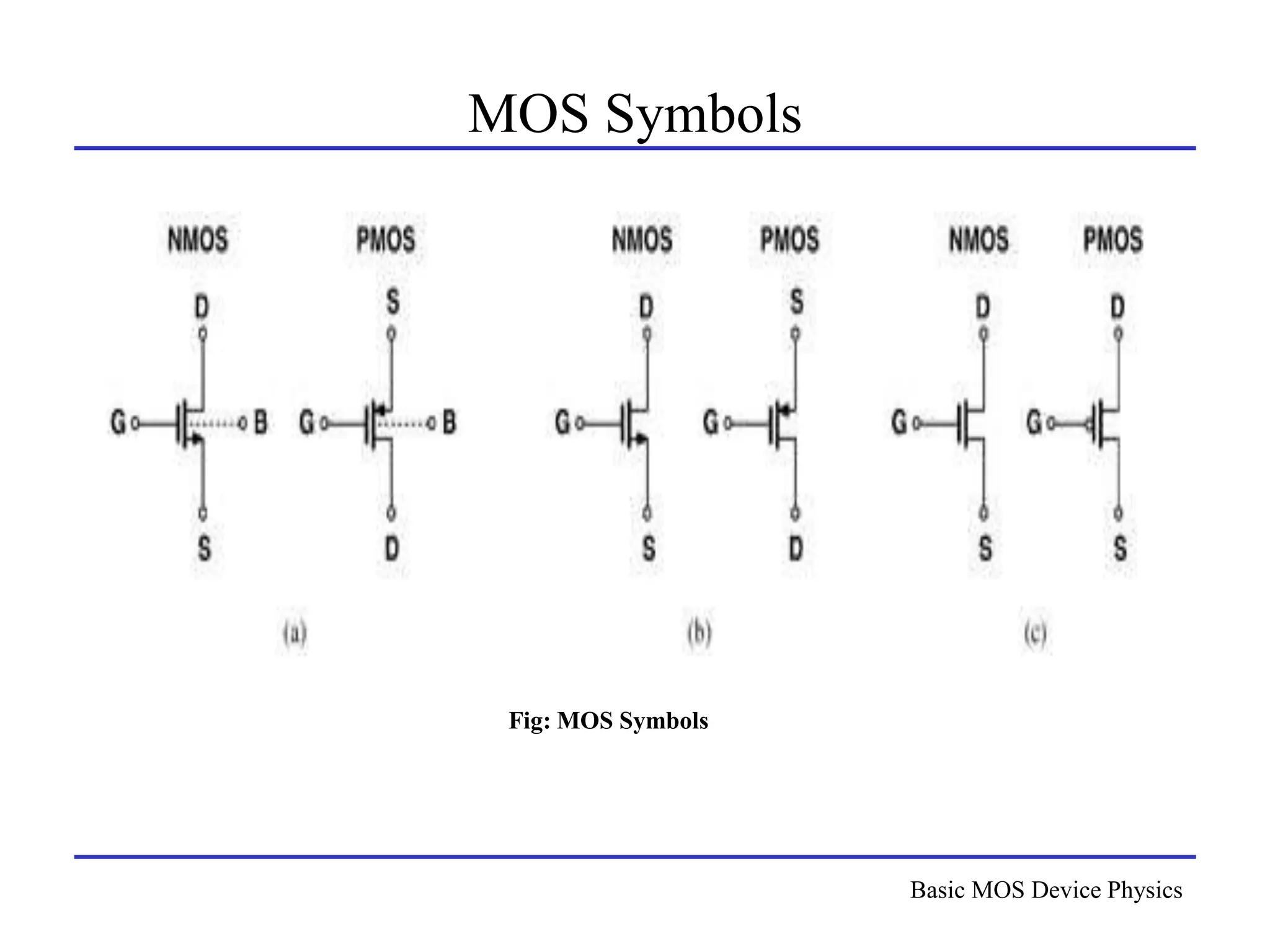
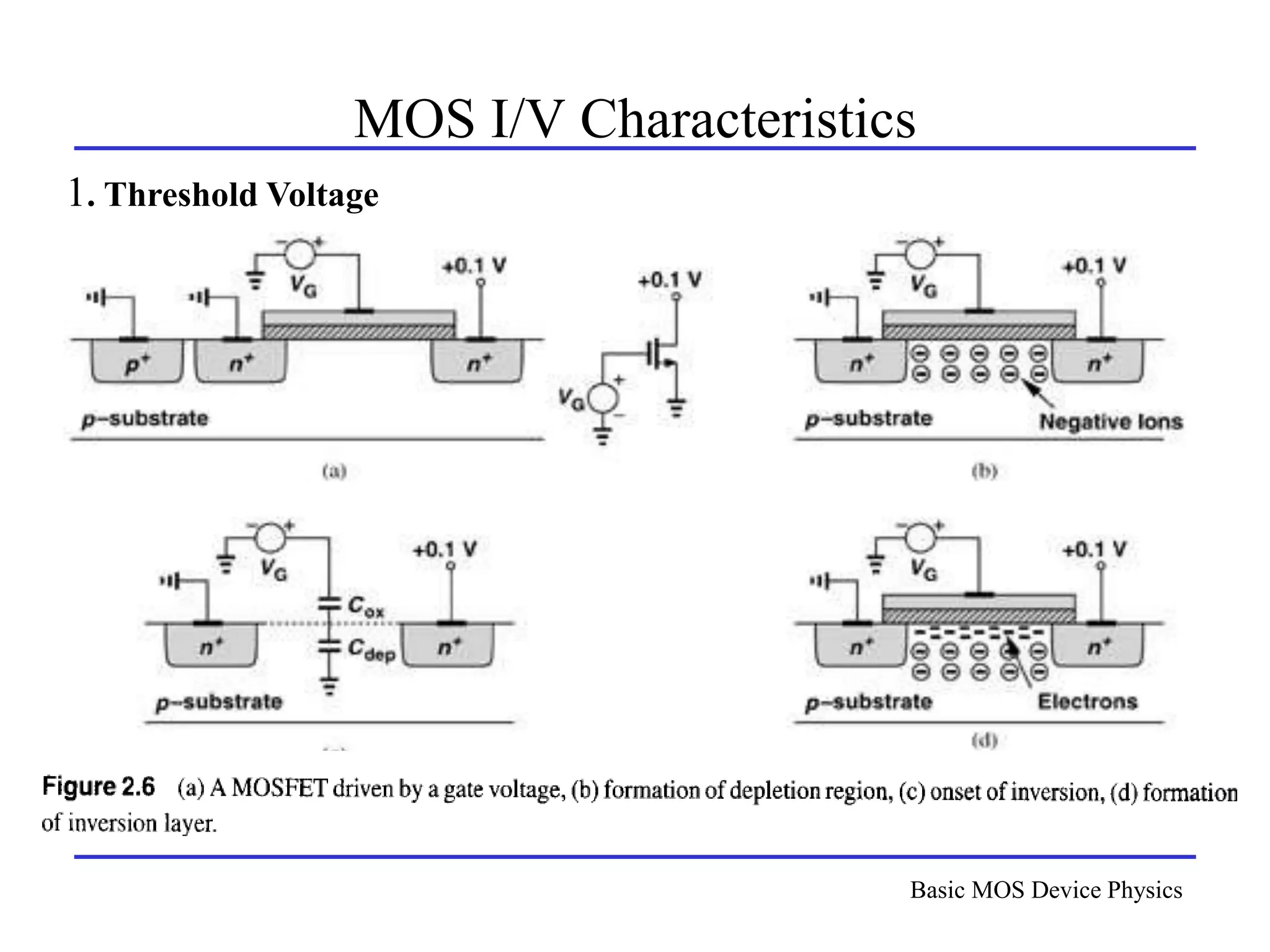
The document covers the fundamental physics and characteristics of MOS devices, including their structure, I/V characteristics, and operation in various regions such as triode and saturation. It also discusses important concepts like transconductance, second-order effects such as body effect and channel length modulation, and includes layout and capacitance considerations. Additionally, it touches on small signal models and SPICE models for MOS simulation.


![Basic MOS Device Physics
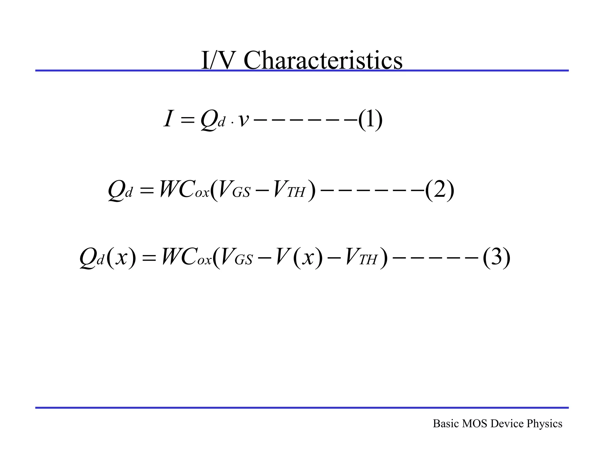
I/V Characteristics (cont.)
)
4
(
]
)
(
[
v
V
x
V
V
WC
I TH
GS
ox
D
)
6
(
]
)
(
[
0
0
VDS
V
TH
GS
n
ox
L
x
D dV
V
x
V
V
WC
dx
I
Given v E and E(x)
dV (x)
dx
)
5
(
)
(
]
)
(
[
dx
x
dV
V
x
V
V
WC
I n
TH
GS
ox
D
)
7
(
]
2
1
)
[( 2
DS
DS
TH
GS
L
W
ox
n
D V
V
V
V
C
I
From eq(1) the current is given by
Using Boundary conditions V(0)=0 and V(L)=Vds](https://image.slidesharecdn.com/unit1ch-01-230514155550-22238e84/75/Unit1-ch-01-ppt-9-2048.jpg)
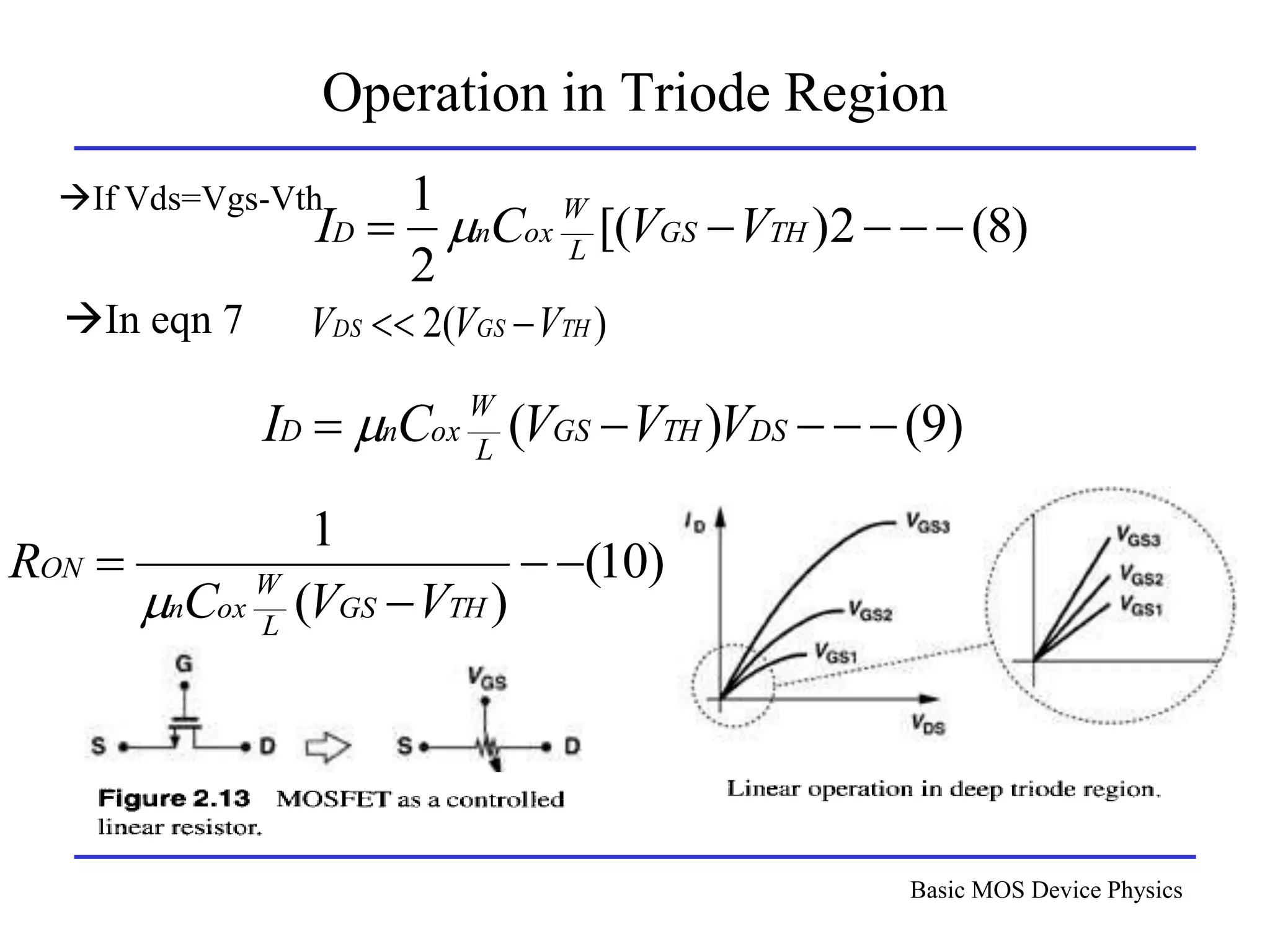
![Basic MOS Device Physics
I/V Characteristics (cont.)
ID nCox
W
L
[(VGS VTH)VDS
1
2
VDS
2
]](https://image.slidesharecdn.com/unit1ch-01-230514155550-22238e84/75/Unit1-ch-01-ppt-10-2048.jpg)

![11
)
)
(
(
)
(
TH
GS
ox
d V
x
V
V
WC
x
Q
Using Boundary conditions for saturated device
)
12
(
]
)
(
[
0
0
VDS
V
TH
GS
n
ox
L
x
D dV
V
x
V
V
WC
dx
I
)
13
(
]
)
(
[
0
0
VTH
VGS
V
TH
GS
n
ox
L
x
D dV
V
x
V
V
WC
dx
I
Limits of left hand side from eqn (12) x=0 to x=L’ and right
hand side frrom V(x)=0 to V(x)=Vgs- Vth](https://image.slidesharecdn.com/unit1ch-01-230514155550-22238e84/75/Unit1-ch-01-ppt-13-2048.jpg)