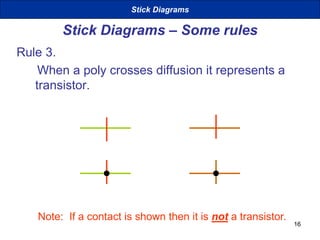
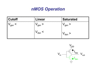
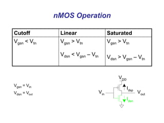
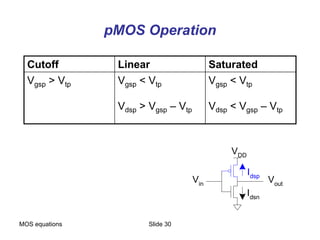
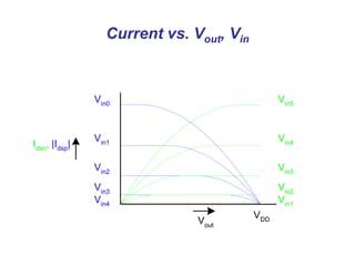
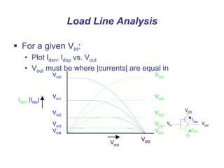
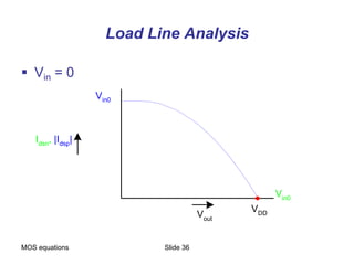
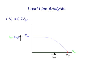
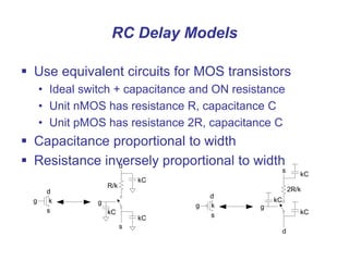
GITAM
(Deemed to be University)
Bengaluru Campus
School of Technology
EEC 401 BASIC VLSI
DESIGN
Presented By
Dr. M. Arun Kumar
Assistant Professor
Department of EECE
Module-3
MOS and BiCMOS Circuit Design Process
Contents
 MOS layers, stick diagrams, design rules and
layout
 CMOS rules
 Layout diagrams, symbolic diagrams
 Basic Circuit concepts
 Sheet resistance
 Area capacitance of layers
 Delay model
 Wiring capacitance
 Choice of layers
 Scaling of MOS circuits
 Scaling models, Scaling function and Limitation of
Scaling
3
MODULE-III
Stick Diagrams
Stick Diagrams
4
PCB Board
5
6
7
Stick Diagrams
N+ N+
Stick Diagrams
8
Stick Diagrams
Gnd
VDD
x x
X
X
X
X
VDD
x x
Gnd
Stick
Diagra
m
Stick Diagrams
9
Stick Diagrams
Gnd
VDD
x x
X
X
X
X
VDD
x x
Gnd
Stick Diagrams
10
Stick Diagrams
 VLSI design aims to translate circuit concepts
onto silicon.
 stick diagrams are a means of capturing
topography and layer information using
simple diagrams.
 Stick diagrams convey layer information
through colour codes (or monochrome
encoding).
 Acts as an interface between symbolic circuit
and the actual layout.
Stick Diagrams
11
Stick Diagrams
 Does show all components/vias.
 It shows relative placement of components.
 Goes one step closer to the layout
 Helps plan the layout and routing
A stick diagram is a cartoon of a layout.
Stick Diagrams
12
Stick Diagrams
 Does not show
• Exact placement of components
• Transistor sizes
• Wire lengths, wire widths, tub boundaries.
• Any other low level details such as parasitics..
Stick Diagrams
13
Stick Diagrams – Notations
Metal 1
poly
ndiff
pdiff
Can also draw
in shades of
gray/line style.
Stick Diagrams
Similarly for contacts, via, tub etc..
14
Stick Diagrams – Some rules
Rule 1.
When two or more ‘sticks’ of the same type cross
or touch each other that represents electrical
contact.
Stick Diagrams
15
Stick Diagrams – Some rules
Rule 2.
When two or more ‘sticks’ of different type cross
or touch each other there is no electrical contact.
(If electrical contact is needed we have to show the connection
explicitly).
Stick Diagrams
16
Stick Diagrams – Some rules
Rule 3.
When a poly crosses diffusion it represents a
transistor.
Note: If a contact is shown then it is not a transistor.
Stick Diagrams
17
Stick Diagrams – Some rules
Rule 4.
In CMOS a demarcation line is drawn to avoid
touching of p-diff with n-diff. All pMOS must lie
on one side of the line and all nMOS will have
to be on the other side.
Stick Diagrams
18
How to draw Stick Diagrams
Stick Diagrams
19
Stick Diagrams
20
Power
Ground
B
C
Out
A
Stick Diagrams
Introduction to
CMOS VLSI
Design
MOS devices: static and
dynamic behavior
Outline
 DC Response
 Logic Levels and Noise Margins
 Transient Response
 Delay Estimation
DC Response
 DC Response: Vout vs. Vin for a gate
 Ex: Inverter
• When Vin = 0 -> Vout = VDD
• When Vin = VDD -> Vout = 0
• In between, Vout depends on
transistor size and current
• By KCL, must settle such that
Idsn = |Idsp|
• We could solve equations
• But graphical solution gives more insight
Idsn
Idsp
Vout
VDD
Vin
Transistor Operation
 Current depends on region of transistor behavior
 For what Vin and Vout are nMOS and pMOS in
• Cutoff?
• Linear?
• Saturation?
nMOS Operation
Cutoff Linear Saturated
Vgsn < Vgsn >
Vdsn <
Vgsn >
Vdsn >
Idsn
Idsp
Vout
VDD
Vin
nMOS Operation
Cutoff Linear Saturated
Vgsn < Vtn Vgsn > Vtn
Vdsn < Vgsn – Vtn
Vgsn > Vtn
Vdsn > Vgsn – Vtn
Idsn
Idsp
Vout
VDD
Vin
nMOS Operation
Cutoff Linear Saturated
Vgsn < Vtn Vgsn > Vtn
Vdsn < Vgsn – Vtn
Vgsn > Vtn
Vdsn > Vgsn – Vtn
Idsn
Idsp
Vout
VDD
Vin
Vgsn = Vin
Vdsn = Vout
nMOS Operation
Cutoff Linear Saturated
Vgsn < Vtn
Vin < Vtn
Vgsn > Vtn
Vin > Vtn
Vdsn < Vgsn – Vtn
Vout < Vin - Vtn
Vgsn > Vtn
Vin > Vtn
Vdsn > Vgsn – Vtn
Vout > Vin - Vtn
Idsn
Idsp
Vout
VDD
Vin
Vgsn = Vin
Vdsn = Vout
pMOS Operation
Cutoff Linear Saturated
Vgsp > Vgsp <
Vdsp >
Vgsp <
Vdsp <
Idsn
Idsp
Vout
VDD
Vin
MOS equations Slide 30
pMOS Operation
Cutoff Linear Saturated
Vgsp > Vtp Vgsp < Vtp
Vdsp > Vgsp – Vtp
Vgsp < Vtp
Vdsp < Vgsp – Vtp
Idsn
Idsp
Vout
VDD
Vin
MOS equations Slide 31
pMOS Operation
Cutoff Linear Saturated
Vgsp > Vtp Vgsp < Vtp
Vdsp > Vgsp – Vtp
Vgsp < Vtp
Vdsp < Vgsp – Vtp
Idsn
Idsp
Vout
VDD
Vin
Vgsp = Vin - VDD
Vdsp = Vout - VDD
Vtp < 0
pMOS Operation
Cutoff Linear Saturated
Vgsp > Vtp
Vin > VDD + Vtp
Vgsp < Vtp
Vin < VDD + Vtp
Vdsp > Vgsp – Vtp
Vout > Vin - Vtp
Vgsp < Vtp
Vin < VDD + Vtp
Vdsp < Vgsp – Vtp
Vout < Vin - Vtp
Idsn
Idsp
Vout
VDD
Vin
Vgsp = Vin - VDD
Vdsp = Vout - VDD
Vtp < 0
I-V Characteristics
 Make pMOS is wider than nMOS such that bn =
bp
Vgsn5
Vgsn4
Vgsn3
Vgsn2
Vgsn1
Vgsp5
Vgsp4
Vgsp3
Vgsp2
Vgsp1
VDD
-VDD
Vdsn
-Vdsp
-Idsp
Idsn
0
Current vs. Vout, Vin
Vin5
Vin4
Vin3
Vin2
Vin1
Vin0
Vin1
Vin2
Vin3
Vin4
Idsn
, |Idsp
|
Vout
VDD
Load Line Analysis
Vin5
Vin4
Vin3
Vin2
Vin1
Vin0
Vin1
Vin2
Vin3
Vin4
Idsn
, |Idsp
|
Vout
VDD
 For a given Vin:
• Plot Idsn, Idsp vs. Vout
• Vout must be where |currents| are equal in
Idsn
Idsp
Vout
VDD
Vin
MOS equations Slide 36
Load Line Analysis
Vin0
Vin0
Idsn
, |Idsp
|
Vout
VDD
 Vin = 0
Load Line Analysis
Vin1
Vin1
Idsn
, |Idsp
|
Vout
VDD
 Vin = 0.2VDD
MOS equations Slide 38
Load Line Analysis
Vin2
Vin2
Idsn
, |Idsp
|
Vout
VDD
 Vin = 0.4VDD
Load Line Analysis
Vin3
Vin3
Idsn
, |Idsp
|
Vout
VDD
 Vin = 0.6VDD
Load Line Analysis
Vin4
Vin4
Idsn
, |Idsp
|
Vout
VDD
 Vin = 0.8VDD
Load Line Analysis
Vin5
Vin0
Vin1
Vin2
Vin3
Vin4
Idsn
, |Idsp
|
Vout
VDD
 Vin = VDD
Load Line Summary
Vin5
Vin4
Vin3
Vin2
Vin1
Vin0
Vin1
Vin2
Vin3
Vin4
Idsn
, |Idsp
|
Vout
VDD
DC Transfer Curve
 Transcribe points onto Vin vs. Vout plot
Vin5
Vin4
Vin3
Vin2
Vin1
Vin0
Vin1
Vin2
Vin3
Vin4
Vout
VDD
C
Vout
0
Vin
VDD
VDD
A B
D
E
Vtn
VDD
/2 VDD
+Vtp
Operating Regions
 Revisit transistor operating regions
C
Vout
0
Vin
VDD
VDD
A B
D
E
Vtn
VDD
/2 VDD
+Vtp
Region nMOS pMOS
A Cutoff Linear
B Saturation Linear
C Saturation Saturation
D Linear Saturation
E Linear Cutoff
Beta Ratio
 If bp / bn  1, switching point will move from
VDD/2
 Called skewed gate
 Other gates: collapse into equivalent inverter
Vout
0
Vin
VDD
VDD
0.5
1
2
10
p
n
b
b

0.1
p
n
b
b

Noise Margins
 How much noise can a gate input see before it
does not recognize the input?
Indeterminate
Region
NML
NMH
Input Characteristics
Output Characteristics
VOH
VDD
VOL
GND
VIH
VIL
Logical High
Input Range
Logical Low
Input Range
Logical High
Output Range
Logical Low
Output Range
Logic Levels
 To maximize noise margins, select logic levels at
VDD
Vin
Vout
VDD
bp
/bn
> 1
Vin
Vout
0
Logic Levels
 To maximize noise margins, select logic levels at
• unity gain point of DC transfer characteristic
VDD
Vin
Vout
VOH
VDD
VOL
VIL
VIH
Vtn
Unity Gain Points
Slope = -1
VDD
-
|Vtp
|
bp
/bn
> 1
Vin
Vout
0
Transient Response
 DC analysis tells us Vout if Vin is constant
 Transient analysis tells us Vout(t) if Vin(t) changes
• Requires solving differential equations
 Input is usually considered to be a step or ramp
• From 0 to VDD or vice versa
Inverter Step Response
 Ex: find step response of inverter driving load
cap
0
( )
(
)
)
(
o
i
ut
n
out
V t t
t
V
t
V
d
d
t

 

Vin(t)
Vout
(t)
Cload
Idsn(t)
Inverter Step Response
 Ex: find step response of inverter driving load
cap
0
0
( )
( )
( )
( )
ou
DD
in
t
out
u t t V
d
d
t
t t
V t
V
V
t





Vin(t)
Vout
(t)
Cload
Idsn(t)
Inverter Step Response
 Ex: find step response of inverter driving load
cap
0
0
(
( )
)
(
(
)
)
DD
D
o
i
D
o t
n
ut
u
V t
u t t V
V
d
d
t
t
V
V
t
t
 



Vin(t)
Vout
(t)
Cload
Idsn(t)
Inverter Step Response
 Ex: find step response of inverter driving load
cap
0
0
( )
( )
( )
(
(
)
)
DD
DD
loa
d
ou
i
d
t
o
n
ut sn
V
V
u t t V
t t
V t
V
d
dt C
t
I t
 

 

0
( ) DD t
out
ou
ds
t DD t
n
I t V V
V
V V
V
t t



  

  

Vin(t)
Vout
(t)
Cload
Idsn(t)
Inverter Step Response
 Ex: find step response of inverter driving load
cap
0
0
( )
( )
( )
(
(
)
)
DD
DD
loa
d
ou
i
d
t
o
n
ut sn
V
V
u t t V
t t
V t
V
d
dt C
t
I t
 

 

 
0
2
2
0
2
)
)
(
( )
( DD DD t
DD
out
out
out out D t
n
t
ds
D
I V
t t
V V V V
V V V V
V
t
V t
V t
b
b




   


 
   
  
 

Vout(t)
Vin(t)
t0
t
Vin(t)
Vout
(t)
Cload
Idsn(t)
Delay Definitions
 tpdr: rising propagation delay
• From input to rising output crossing VDD/2
 tpdf: falling propagation delay
• From input to falling output crossing VDD/2
 tpd: average propagation delay
• tpd = (tpdr + tpdf)/2
 tr: rise time
• From output crossing 0.2 VDD to 0.8 VDD
 tf: fall time
• From output crossing 0.8 VDD to 0.2 VDD
Delay Definitions
 tcdr: rising contamination delay
• From input to rising output crossing VDD/2
 tcdf: falling contamination delay
• From input to falling output crossing VDD/2
 tcd: average contamination delay
• tpd = (tcdr + tcdf)/2
Simulated Inverter Delay
 Solving differential equations by hand is too hard
 SPICE simulator solves the equations
numerically
• Uses more accurate I-V models too!
 But simulations take time to write
(V)
0.0
0.5
1.0
1.5
2.0
t(s)
0.0 200p 400p 600p 800p 1n
tpdf
= 66ps tpdr
= 83ps
Vin
Vout
Delay Estimation
 We would like to be able to easily estimate delay
• Not as accurate as simulation
• But easier to ask “What if?”
 The step response usually looks like a 1st order
RC response with a decaying exponential.
 Use RC delay models to estimate delay
• C = total capacitance on output node
• Use effective resistance R
• So that tpd = RC
 Characterize transistors by finding their effective
R
• Depends on average current as gate switches
RC Delay Models
 Use equivalent circuits for MOS transistors
• Ideal switch + capacitance and ON resistance
• Unit nMOS has resistance R, capacitance C
• Unit pMOS has resistance 2R, capacitance C
 Capacitance proportional to width
 Resistance inversely proportional to width
k
g
s
d
g
s
d
kC
kC
kC
R/k
k
g
s
d
g
s
d
kC
kC
kC
2R/k
Delay Components
 Delay has two parts
• Parasitic delay
 6 or 7 RC
 Independent of load
• Effort delay
 4h RC
 Proportional to load capacitance
7C
3C
3C
3
3
3
2
2
2
3C
2C
2C
3C
3C
Isolated
Contacted
Diffusion
Merged
Uncontacted
Diffusion
Shared
Contacted
Diffusion
Diffusion Capacitance
 we assumed contacted diffusion on every s / d.
 Good layout minimizes diffusion area
 Ex: NAND3 layout shares one diffusion contact
• Reduces output capacitance by 2C
• Merged uncontacted diffusion might help too

Stick diagram with EEC 401 Basic VLSI Design.ppt

  • 1.
    GITAM (Deemed to beUniversity) Bengaluru Campus School of Technology EEC 401 BASIC VLSI DESIGN Presented By Dr. M. Arun Kumar Assistant Professor Department of EECE
  • 2.
    Module-3 MOS and BiCMOSCircuit Design Process Contents  MOS layers, stick diagrams, design rules and layout  CMOS rules  Layout diagrams, symbolic diagrams  Basic Circuit concepts  Sheet resistance  Area capacitance of layers  Delay model  Wiring capacitance  Choice of layers  Scaling of MOS circuits  Scaling models, Scaling function and Limitation of Scaling
  • 3.
  • 4.
  • 5.
  • 6.
  • 7.
  • 8.
    8 Stick Diagrams Gnd VDD x x X X X X VDD xx Gnd Stick Diagra m Stick Diagrams
  • 9.
  • 10.
    10 Stick Diagrams  VLSIdesign aims to translate circuit concepts onto silicon.  stick diagrams are a means of capturing topography and layer information using simple diagrams.  Stick diagrams convey layer information through colour codes (or monochrome encoding).  Acts as an interface between symbolic circuit and the actual layout. Stick Diagrams
  • 11.
    11 Stick Diagrams  Doesshow all components/vias.  It shows relative placement of components.  Goes one step closer to the layout  Helps plan the layout and routing A stick diagram is a cartoon of a layout. Stick Diagrams
  • 12.
    12 Stick Diagrams  Doesnot show • Exact placement of components • Transistor sizes • Wire lengths, wire widths, tub boundaries. • Any other low level details such as parasitics.. Stick Diagrams
  • 13.
    13 Stick Diagrams –Notations Metal 1 poly ndiff pdiff Can also draw in shades of gray/line style. Stick Diagrams Similarly for contacts, via, tub etc..
  • 14.
    14 Stick Diagrams –Some rules Rule 1. When two or more ‘sticks’ of the same type cross or touch each other that represents electrical contact. Stick Diagrams
  • 15.
    15 Stick Diagrams –Some rules Rule 2. When two or more ‘sticks’ of different type cross or touch each other there is no electrical contact. (If electrical contact is needed we have to show the connection explicitly). Stick Diagrams
  • 16.
    16 Stick Diagrams –Some rules Rule 3. When a poly crosses diffusion it represents a transistor. Note: If a contact is shown then it is not a transistor. Stick Diagrams
  • 17.
    17 Stick Diagrams –Some rules Rule 4. In CMOS a demarcation line is drawn to avoid touching of p-diff with n-diff. All pMOS must lie on one side of the line and all nMOS will have to be on the other side. Stick Diagrams
  • 18.
    18 How to drawStick Diagrams Stick Diagrams
  • 19.
  • 20.
  • 21.
    Introduction to CMOS VLSI Design MOSdevices: static and dynamic behavior
  • 22.
    Outline  DC Response Logic Levels and Noise Margins  Transient Response  Delay Estimation
  • 23.
    DC Response  DCResponse: Vout vs. Vin for a gate  Ex: Inverter • When Vin = 0 -> Vout = VDD • When Vin = VDD -> Vout = 0 • In between, Vout depends on transistor size and current • By KCL, must settle such that Idsn = |Idsp| • We could solve equations • But graphical solution gives more insight Idsn Idsp Vout VDD Vin
  • 24.
    Transistor Operation  Currentdepends on region of transistor behavior  For what Vin and Vout are nMOS and pMOS in • Cutoff? • Linear? • Saturation?
  • 25.
    nMOS Operation Cutoff LinearSaturated Vgsn < Vgsn > Vdsn < Vgsn > Vdsn > Idsn Idsp Vout VDD Vin
  • 26.
    nMOS Operation Cutoff LinearSaturated Vgsn < Vtn Vgsn > Vtn Vdsn < Vgsn – Vtn Vgsn > Vtn Vdsn > Vgsn – Vtn Idsn Idsp Vout VDD Vin
  • 27.
    nMOS Operation Cutoff LinearSaturated Vgsn < Vtn Vgsn > Vtn Vdsn < Vgsn – Vtn Vgsn > Vtn Vdsn > Vgsn – Vtn Idsn Idsp Vout VDD Vin Vgsn = Vin Vdsn = Vout
  • 28.
    nMOS Operation Cutoff LinearSaturated Vgsn < Vtn Vin < Vtn Vgsn > Vtn Vin > Vtn Vdsn < Vgsn – Vtn Vout < Vin - Vtn Vgsn > Vtn Vin > Vtn Vdsn > Vgsn – Vtn Vout > Vin - Vtn Idsn Idsp Vout VDD Vin Vgsn = Vin Vdsn = Vout
  • 29.
    pMOS Operation Cutoff LinearSaturated Vgsp > Vgsp < Vdsp > Vgsp < Vdsp < Idsn Idsp Vout VDD Vin
  • 30.
    MOS equations Slide30 pMOS Operation Cutoff Linear Saturated Vgsp > Vtp Vgsp < Vtp Vdsp > Vgsp – Vtp Vgsp < Vtp Vdsp < Vgsp – Vtp Idsn Idsp Vout VDD Vin
  • 31.
    MOS equations Slide31 pMOS Operation Cutoff Linear Saturated Vgsp > Vtp Vgsp < Vtp Vdsp > Vgsp – Vtp Vgsp < Vtp Vdsp < Vgsp – Vtp Idsn Idsp Vout VDD Vin Vgsp = Vin - VDD Vdsp = Vout - VDD Vtp < 0
  • 32.
    pMOS Operation Cutoff LinearSaturated Vgsp > Vtp Vin > VDD + Vtp Vgsp < Vtp Vin < VDD + Vtp Vdsp > Vgsp – Vtp Vout > Vin - Vtp Vgsp < Vtp Vin < VDD + Vtp Vdsp < Vgsp – Vtp Vout < Vin - Vtp Idsn Idsp Vout VDD Vin Vgsp = Vin - VDD Vdsp = Vout - VDD Vtp < 0
  • 33.
    I-V Characteristics  MakepMOS is wider than nMOS such that bn = bp Vgsn5 Vgsn4 Vgsn3 Vgsn2 Vgsn1 Vgsp5 Vgsp4 Vgsp3 Vgsp2 Vgsp1 VDD -VDD Vdsn -Vdsp -Idsp Idsn 0
  • 34.
    Current vs. Vout,Vin Vin5 Vin4 Vin3 Vin2 Vin1 Vin0 Vin1 Vin2 Vin3 Vin4 Idsn , |Idsp | Vout VDD
  • 35.
    Load Line Analysis Vin5 Vin4 Vin3 Vin2 Vin1 Vin0 Vin1 Vin2 Vin3 Vin4 Idsn ,|Idsp | Vout VDD  For a given Vin: • Plot Idsn, Idsp vs. Vout • Vout must be where |currents| are equal in Idsn Idsp Vout VDD Vin
  • 36.
    MOS equations Slide36 Load Line Analysis Vin0 Vin0 Idsn , |Idsp | Vout VDD  Vin = 0
  • 37.
    Load Line Analysis Vin1 Vin1 Idsn ,|Idsp | Vout VDD  Vin = 0.2VDD
  • 38.
    MOS equations Slide38 Load Line Analysis Vin2 Vin2 Idsn , |Idsp | Vout VDD  Vin = 0.4VDD
  • 39.
    Load Line Analysis Vin3 Vin3 Idsn ,|Idsp | Vout VDD  Vin = 0.6VDD
  • 40.
    Load Line Analysis Vin4 Vin4 Idsn ,|Idsp | Vout VDD  Vin = 0.8VDD
  • 41.
  • 42.
  • 43.
    DC Transfer Curve Transcribe points onto Vin vs. Vout plot Vin5 Vin4 Vin3 Vin2 Vin1 Vin0 Vin1 Vin2 Vin3 Vin4 Vout VDD C Vout 0 Vin VDD VDD A B D E Vtn VDD /2 VDD +Vtp
  • 44.
    Operating Regions  Revisittransistor operating regions C Vout 0 Vin VDD VDD A B D E Vtn VDD /2 VDD +Vtp Region nMOS pMOS A Cutoff Linear B Saturation Linear C Saturation Saturation D Linear Saturation E Linear Cutoff
  • 45.
    Beta Ratio  Ifbp / bn  1, switching point will move from VDD/2  Called skewed gate  Other gates: collapse into equivalent inverter Vout 0 Vin VDD VDD 0.5 1 2 10 p n b b  0.1 p n b b 
  • 46.
    Noise Margins  Howmuch noise can a gate input see before it does not recognize the input? Indeterminate Region NML NMH Input Characteristics Output Characteristics VOH VDD VOL GND VIH VIL Logical High Input Range Logical Low Input Range Logical High Output Range Logical Low Output Range
  • 47.
    Logic Levels  Tomaximize noise margins, select logic levels at VDD Vin Vout VDD bp /bn > 1 Vin Vout 0
  • 48.
    Logic Levels  Tomaximize noise margins, select logic levels at • unity gain point of DC transfer characteristic VDD Vin Vout VOH VDD VOL VIL VIH Vtn Unity Gain Points Slope = -1 VDD - |Vtp | bp /bn > 1 Vin Vout 0
  • 49.
    Transient Response  DCanalysis tells us Vout if Vin is constant  Transient analysis tells us Vout(t) if Vin(t) changes • Requires solving differential equations  Input is usually considered to be a step or ramp • From 0 to VDD or vice versa
  • 50.
    Inverter Step Response Ex: find step response of inverter driving load cap 0 ( ) ( ) ) ( o i ut n out V t t t V t V d d t     Vin(t) Vout (t) Cload Idsn(t)
  • 51.
    Inverter Step Response Ex: find step response of inverter driving load cap 0 0 ( ) ( ) ( ) ( ) ou DD in t out u t t V d d t t t V t V V t      Vin(t) Vout (t) Cload Idsn(t)
  • 52.
    Inverter Step Response Ex: find step response of inverter driving load cap 0 0 ( ( ) ) ( ( ) ) DD D o i D o t n ut u V t u t t V V d d t t V V t t      Vin(t) Vout (t) Cload Idsn(t)
  • 53.
    Inverter Step Response Ex: find step response of inverter driving load cap 0 0 ( ) ( ) ( ) ( ( ) ) DD DD loa d ou i d t o n ut sn V V u t t V t t V t V d dt C t I t       0 ( ) DD t out ou ds t DD t n I t V V V V V V t t            Vin(t) Vout (t) Cload Idsn(t)
  • 54.
    Inverter Step Response Ex: find step response of inverter driving load cap 0 0 ( ) ( ) ( ) ( ( ) ) DD DD loa d ou i d t o n ut sn V V u t t V t t V t V d dt C t I t         0 2 2 0 2 ) ) ( ( ) ( DD DD t DD out out out out D t n t ds D I V t t V V V V V V V V V t V t V t b b                       Vin(t) Vout (t) Cload Idsn(t)
  • 55.
    Inverter Step Response Ex: find step response of inverter driving load cap 0 0 ( ) ( ) ( ) ( ( ) ) DD DD loa d ou i d t o n ut sn V V u t t V t t V t V d dt C t I t         0 2 2 0 2 ) ) ( ( ) ( DD DD t DD out out out out D t n t ds D I V t t V V V V V V V V V t V t V t b b                       Vout(t) Vin(t) t0 t Vin(t) Vout (t) Cload Idsn(t)
  • 56.
    Delay Definitions  tpdr:rising propagation delay • From input to rising output crossing VDD/2  tpdf: falling propagation delay • From input to falling output crossing VDD/2  tpd: average propagation delay • tpd = (tpdr + tpdf)/2  tr: rise time • From output crossing 0.2 VDD to 0.8 VDD  tf: fall time • From output crossing 0.8 VDD to 0.2 VDD
  • 57.
    Delay Definitions  tcdr:rising contamination delay • From input to rising output crossing VDD/2  tcdf: falling contamination delay • From input to falling output crossing VDD/2  tcd: average contamination delay • tpd = (tcdr + tcdf)/2
  • 58.
    Simulated Inverter Delay Solving differential equations by hand is too hard  SPICE simulator solves the equations numerically • Uses more accurate I-V models too!  But simulations take time to write (V) 0.0 0.5 1.0 1.5 2.0 t(s) 0.0 200p 400p 600p 800p 1n tpdf = 66ps tpdr = 83ps Vin Vout
  • 59.
    Delay Estimation  Wewould like to be able to easily estimate delay • Not as accurate as simulation • But easier to ask “What if?”  The step response usually looks like a 1st order RC response with a decaying exponential.  Use RC delay models to estimate delay • C = total capacitance on output node • Use effective resistance R • So that tpd = RC  Characterize transistors by finding their effective R • Depends on average current as gate switches
  • 60.
    RC Delay Models Use equivalent circuits for MOS transistors • Ideal switch + capacitance and ON resistance • Unit nMOS has resistance R, capacitance C • Unit pMOS has resistance 2R, capacitance C  Capacitance proportional to width  Resistance inversely proportional to width k g s d g s d kC kC kC R/k k g s d g s d kC kC kC 2R/k
  • 61.
    Delay Components  Delayhas two parts • Parasitic delay  6 or 7 RC  Independent of load • Effort delay  4h RC  Proportional to load capacitance
  • 62.
    7C 3C 3C 3 3 3 2 2 2 3C 2C 2C 3C 3C Isolated Contacted Diffusion Merged Uncontacted Diffusion Shared Contacted Diffusion Diffusion Capacitance  weassumed contacted diffusion on every s / d.  Good layout minimizes diffusion area  Ex: NAND3 layout shares one diffusion contact • Reduces output capacitance by 2C • Merged uncontacted diffusion might help too