Downloaded 385 times
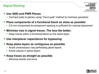

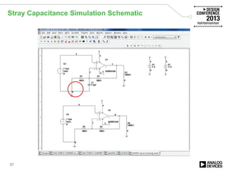
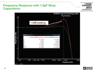
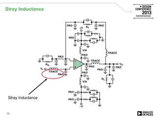
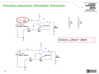

The document provides guidelines and techniques for high-speed PCB design, emphasizing proper component placement, signal routing, and power supply bypassing to enhance circuit performance. It discusses the importance of effective schematics, the selection of materials, and considerations for minimizing parasitics and crosstalk. Additionally, it covers legal disclaimers regarding the proprietary nature of the content and lists a structured agenda outlining the key topics addressed.


![Signal Integrity - A Crash Course [R Lott]](https://cdn.slidesharecdn.com/ss_thumbnails/1cb0870c-cad3-4a68-ad41-8e9450fec5d8-170217191645-thumbnail.jpg?width=640&height=640&fit=bounds)