Download as PDF, PPTX


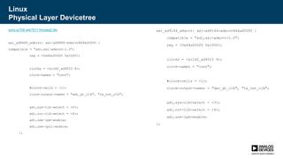


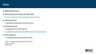
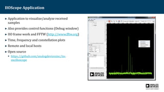
![Linux IIO
► Lots of information online
https://wiki.analog.com/resources/tools-
software/linux-software/libiio
► Application is independent of back end
Ethernet, USB, Serial etc.
iio_channel_read(,, &received_samples[0], );
iio_channel_write(,, &transmit_samples[0],);
Figurative only, actual function call and parameters
may vary
► The IIOScope application in the demo is running
FFTW on the received samples using the IIO
framework](https://image.slidesharecdn.com/jesd204binterfaceframeworktechnicalinstruction-180322191137/85/AD-IP-JESD204-JESD204B-Interface-Framework-78-320.jpg)
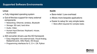
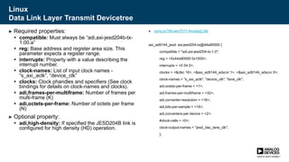
![No-OS (Bare Metal)
► Simple generic ‘C’
► Mostly duplicated Kernel Drivers
► Proof of concept/Sanity checking
► Maintained and released with HDL & Linux
https://github.com/analogdevicesinc/no-OS
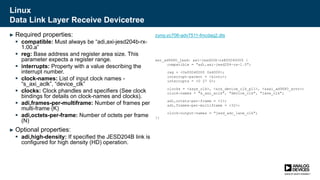
► Capture is possible but usually requires the tool
to off load samples
► Linux is recommended for its shear capability
and ease of use
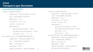
// adc device-clk-sysref, fpga-clk-sysref
ad9523_channels[ADC_DEVICE_CLK].channel_num = 13;
ad9523_channels[ADC_DEVICE_CLK].channel_divider = 1;
ad9523_channels[ADC_DEVICE_SYSREF].channel_num = 6;
ad9523_channels[ADC_DEVICE_SYSREF].channel_divider = 128;
ad9144_channels[0].dds_frequency_0 = 11*1000*1000;
ad9144_channels[0].sel = DAC_SRC_DDS;
ad9680_setup(&ad9680_spi_device, ad9680_param);
jesd_setup(ad9680_jesd);
xcvr_setup(ad9680_xcvr);
jesd_status(ad9680_jesd);
adc_setup(ad9680_core);](https://image.slidesharecdn.com/jesd204binterfaceframeworktechnicalinstruction-180322191137/85/AD-IP-JESD204-JESD204B-Interface-Framework-80-320.jpg)


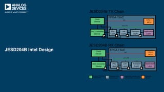
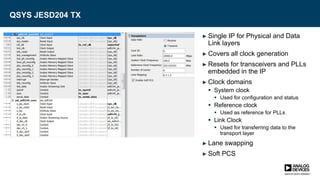
The document discusses the JESD204B interface framework designed for high-speed serial communication between data converters and FPGAs, highlighting its layers, components, and design issues related to implementation. It emphasizes the framework's automatic configuration capabilities to manage complexity, improve diagnostics, and facilitate application-driven design, while addressing challenges of high-speed links. Furthermore, it outlines the integration of hardware, HDL, and software elements, aimed at simplifying interoperability and enhancing system-level performance.