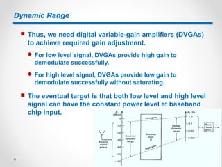
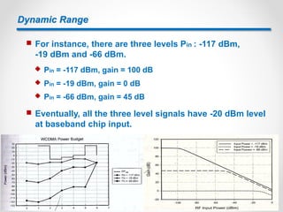
Dynamic range is an important consideration for digital receivers. A high dynamic range allows a receiver to capture both weak and strong signals. Digital variable gain amplifiers provide gain adjustment to keep signal levels constant at the analog-to-digital converter (ADC) input. Factors like modulation type, noise, distortion, and peak-to-average power ratio determine the required ADC dynamic range. Proper automatic gain control and oversampling can help improve dynamic range performance.

![Dynamic Range
Digital receivers for cellular communications require
the highest performance from analog-to-digital
converters (ADCs) and their supporting cast of RF
components[39].
The signal chain must be sensitive enough to capture
low-level signals, while providing enough linearity to
handle high-level interfering signals (blockers). That is,
its dynamic range ought to be high enough.](https://image.slidesharecdn.com/theabcsofadcsunderstandinghowadcerrorsaffectsystemperformance-161130141210/85/The-ABCs-of-ADCs-Understanding-How-ADC-Errors-Affect-System-Performance-2-320.jpg)


![AGC
In receiver applications, the lower level desired signal is
digitized alone or in the presence of an unwanted
signal(s) that can be significantly larger in
amplitude[39].
Thus, stringent noise and distortion requirements are
placed on the ADC
The converter's noise figure(NF) is determined by
comparing its total noise power to the thermal noise
floor. For small analog input signals, the thermal +
quantization noise power dominate the ADC‘s noise
floor, which is used to approximate the ADC's effective
NF[39].](https://image.slidesharecdn.com/theabcsofadcsunderstandinghowadcerrorsaffectsystemperformance-161130141210/85/The-ABCs-of-ADCs-Understanding-How-ADC-Errors-Affect-System-Performance-5-320.jpg)
![AGC
In general, the ADC often doesn’t have sufficient
dynamic range to meet both the NF requirements
(receiver sensitivity ) and maximum blocker
requirements without implementing automatic gain
control (AGC). The AGC can be included either in the
RF stages, IF stages, or both.
ADCs are optimized for baseband performance where
the input frequency (fINPUT) is less than one-half the
clock frequency (fCLOCK/2). Operating in this frequency
range and using these baseband-optimized parts
provide the optimal possible ADCs’ dynamic range[39].](https://image.slidesharecdn.com/theabcsofadcsunderstandinghowadcerrorsaffectsystemperformance-161130141210/85/The-ABCs-of-ADCs-Understanding-How-ADC-Errors-Affect-System-Performance-6-320.jpg)
![AGC
In practice, once the ADC's effective NF is known under
small-signal conditions, and the cascaded NF of the
analog (RF and IF) circuitry is determined, the minimum
power gain ahead of the ADC is selected to meet the
required receiver NF.
The amount of power gain places an upper limit on the
maximum blocker, or highest interference level the
receiver can tolerate before the ADC overloads[39,45].](https://image.slidesharecdn.com/theabcsofadcsunderstandinghowadcerrorsaffectsystemperformance-161130141210/85/The-ABCs-of-ADCs-Understanding-How-ADC-Errors-Affect-System-Performance-7-320.jpg)
![AGC
The photo shown below depicts the ADC noise
contribution in the absence of a large-level blocker. An
overall gain of 36 dB is needed to achieve the desired
cascaded receiver NF of 3.7 dB[39].](https://image.slidesharecdn.com/theabcsofadcsunderstandinghowadcerrorsaffectsystemperformance-161130141210/85/The-ABCs-of-ADCs-Understanding-How-ADC-Errors-Affect-System-Performance-8-320.jpg)
![AGC
With 36-dB gain ahead of the ADC, a maximum single
tone blocker level above −30dBm at the antenna
terminal will exceed the ADC full-scale. Thus, a 6-dB
gain reduction was used to increase the largest
allowable blocker signal applied to the ADC providing
margin to the standard's specification[39].](https://image.slidesharecdn.com/theabcsofadcsunderstandinghowadcerrorsaffectsystemperformance-161130141210/85/The-ABCs-of-ADCs-Understanding-How-ADC-Errors-Affect-System-Performance-9-320.jpg)
![ENOB
Using a 12-bit-resolution analog-to-digital converter
(ADC) does not necessarily mean your system will
have 12-bit accuracy[44].
Perhaps you only obtain an Effective Number Of
Bits(ENOB) value of 11 eventually. Therefore,
you have lost 1 bit of information due to the converter's
noise and distortion performance[44].](https://image.slidesharecdn.com/theabcsofadcsunderstandinghowadcerrorsaffectsystemperformance-161130141210/85/The-ABCs-of-ADCs-Understanding-How-ADC-Errors-Affect-System-Performance-10-320.jpg)
![Oversample
One way to improve SNR is to oversample, which
provides a processing gain. Oversampling is a method
of lowering the noise floor of the converter by sampling
at a rate much higher than the signal of interest. This
spreads the noise out over a wider range in the
frequency domain, thereby effectively reducing the
noise at any one frequency bin. A 2X oversampling
reduces the noise floor by 3dB[40,44].
Noise floor
reduction](https://image.slidesharecdn.com/theabcsofadcsunderstandinghowadcerrorsaffectsystemperformance-161130141210/85/The-ABCs-of-ADCs-Understanding-How-ADC-Errors-Affect-System-Performance-11-320.jpg)
![SFDR
In RF design, two definitions of dynamic range have
emerged. The first, simply called the dynamic range,
refers to the maximum tolerable desired signal power
divided by the minimum tolerable desired signal power
(the sensitivity). That is, it is limited by compression at
the upper end and noise at the lower end[46].
Level
FrequencyNoise Floor
Sensitivity
Compression
Point
Dynamic Range](https://image.slidesharecdn.com/theabcsofadcsunderstandinghowadcerrorsaffectsystemperformance-161130141210/85/The-ABCs-of-ADCs-Understanding-How-ADC-Errors-Affect-System-Performance-12-320.jpg)
![SFDR
Another term often used to describe the dynamic range
is the spurious free dynamic range (SFDR), which is the
level at which the intermodulation distortion (IMD)
products are equal to the noise floor[46,47].
Therefore, the input signals are adjusted such that the
difference between the desired signals and the noise
floor is equal to the difference between the desired
signals and the spurs.
Level
FrequencyNoise Floor
Sensitivity
SFDR
2f1-f2 2f2-f1f1 f2](https://image.slidesharecdn.com/theabcsofadcsunderstandinghowadcerrorsaffectsystemperformance-161130141210/85/The-ABCs-of-ADCs-Understanding-How-ADC-Errors-Affect-System-Performance-13-320.jpg)
![SFDR
In terms of ADC, SFDR is defined as the ratio of the
signal to the largest spur observed in the frequency
domain using an FFT plot.
Spurs prevent the ADC from converting small input
signals, because the distortion component can be
much larger than the signal of interest.
This limits the dynamic range of the ADC. Note that a
large spur in the frequency domain may not
significantly affect the SNR, but will significantly affect
the SFDR[44].](https://image.slidesharecdn.com/theabcsofadcsunderstandinghowadcerrorsaffectsystemperformance-161130141210/85/The-ABCs-of-ADCs-Understanding-How-ADC-Errors-Affect-System-Performance-14-320.jpg)
![SFDR
FFT plot reveals performance of an ADC[44] :](https://image.slidesharecdn.com/theabcsofadcsunderstandinghowadcerrorsaffectsystemperformance-161130141210/85/The-ABCs-of-ADCs-Understanding-How-ADC-Errors-Affect-System-Performance-15-320.jpg)
![SFDR
SFDR of the ADC limits the detection of low-input
signals[36]:](https://image.slidesharecdn.com/theabcsofadcsunderstandinghowadcerrorsaffectsystemperformance-161130141210/85/The-ABCs-of-ADCs-Understanding-How-ADC-Errors-Affect-System-Performance-16-320.jpg)
![SFDR
A interferer located inside the bandwidth of interest
can’t be filtered out. It haves the signal chain reduce
the gain so that the ADC doesn’t get saturated. Less
gain in the signal chain reduces the ability to elevate
small signals(as shown above, “Wanted Signal B”)
above the ADC noise floor to properly detect it.
Harmonic spurs of the in-band interferer also can fall on
top of the wanted signal, limiting the sensitivity of the
receiver[36].
Therefore, reduction in SFDR doesn’t affect SNR, but
affects dynamic range, thereby aggravating
sensitivity[36].](https://image.slidesharecdn.com/theabcsofadcsunderstandinghowadcerrorsaffectsystemperformance-161130141210/85/The-ABCs-of-ADCs-Understanding-How-ADC-Errors-Affect-System-Performance-17-320.jpg)
![SFDR of differential ADC
Most high-speed ADCs use a differential input
structure, which provides good common-mode noise
rejection capability[43,48].](https://image.slidesharecdn.com/theabcsofadcsunderstandinghowadcerrorsaffectsystemperformance-161130141210/85/The-ABCs-of-ADCs-Understanding-How-ADC-Errors-Affect-System-Performance-18-320.jpg)
![SFDR of differential ADC
Nevertheless, in practice, there may be some small
differential imbalances that distort the signal of interest
and decrease the SFDR through the ADC[43].
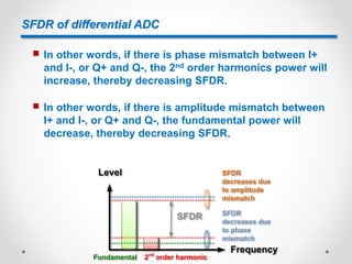
Phase mismatch between each side of the differential
input signal at the front end of the ADC creates an
increase in harmonics power. This can happen when
one side of the differential signal leads the other side in
time by some amount of phase relative to its period[43].](https://image.slidesharecdn.com/theabcsofadcsunderstandinghowadcerrorsaffectsystemperformance-161130141210/85/The-ABCs-of-ADCs-Understanding-How-ADC-Errors-Affect-System-Performance-19-320.jpg)
![SFDR of differential ADC
The differential structure is designed to suppress even
order distortion. As shown below, with differential
operation, the 2nd order harmonics distortion (HD2)
is much lower than single-ended one[49].
Thus, as mentioned above, phase mismatch creates an
increase in harmonics power, especially HD2, thereby
decreasing SFDR[43].
Level
Frequency
SFDR
Fundamental 2nd
order harmonics](https://image.slidesharecdn.com/theabcsofadcsunderstandinghowadcerrorsaffectsystemperformance-161130141210/85/The-ABCs-of-ADCs-Understanding-How-ADC-Errors-Affect-System-Performance-20-320.jpg)
![SFDR of differential ADC
Another imbalance at the front end of a differential
signal can be amplitude mismatch. When one side
of a differential signal has a different gain than its
complement, the ADC input sees one side as a larger
signal and the other as a smaller signal[43].
This otherwise reduces the full power of the
fundamental signal and decreases the SFDR in dBc.
A 2-dB amplitude mismatch between differential inputs
will result in a 1-dB full-scale reduction in the power of
the input signal.](https://image.slidesharecdn.com/theabcsofadcsunderstandinghowadcerrorsaffectsystemperformance-161130141210/85/The-ABCs-of-ADCs-Understanding-How-ADC-Errors-Affect-System-Performance-21-320.jpg)

![Radio and Data Converter Functions
The radio lineup used in a typical mobile
application[40] :](https://image.slidesharecdn.com/theabcsofadcsunderstandinghowadcerrorsaffectsystemperformance-161130141210/85/The-ABCs-of-ADCs-Understanding-How-ADC-Errors-Affect-System-Performance-23-320.jpg)
![Radio and Data Converter Functions
The radio architecture, a ZIF receiver requires a dual-
channel high-speed Rx ADC for in-phase and
quadrature-phase (I/Q) baseband signal sampling
and construction[40].
The digital baseband processor performs signal-
processing functions like channel coding, modulation
mapping, and digital filtering[40].](https://image.slidesharecdn.com/theabcsofadcsunderstandinghowadcerrorsaffectsystemperformance-161130141210/85/The-ABCs-of-ADCs-Understanding-How-ADC-Errors-Affect-System-Performance-24-320.jpg)
![High-Speed Analog Front-End (AFE)
Primarily, the converter’s dynamic performance
establishes the radio’s performance level. The Rx ADC
must faithfully digitize and synthesize receiver signals
without degrading system SNR[40].
System requirements for modulation order, desired
BER, undesired high interference levels, and spurious
emission levels determine the Rx ADC dynamic
specifications. Signals that use high-order modulation
require more quantization levels. Channel bandwidth
determines the converter sample rate. The signal peak-
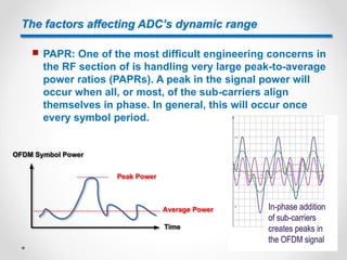
to-average power ratio (PAPR) dictates dynamic range,
and system spurious emission limits determine output
spectral purity[40].](https://image.slidesharecdn.com/theabcsofadcsunderstandinghowadcerrorsaffectsystemperformance-161130141210/85/The-ABCs-of-ADCs-Understanding-How-ADC-Errors-Affect-System-Performance-25-320.jpg)
![High-Speed Converter Sample Rate
The Nyquist criterion dictates that converter sampling
frequency must be at least twice the highest frequency
component of interest or information will be
lost[40].
For example, in an 802.11g WiFi, the channel bandwidth
is 16.25MHz. At baseband, the I/Q frequency
components are each 8.125MHz. So theoretically, the Rx
ADC must sample at least 16.25Msps (FCLK =
16.25MHz)[40].](https://image.slidesharecdn.com/theabcsofadcsunderstandinghowadcerrorsaffectsystemperformance-161130141210/85/The-ABCs-of-ADCs-Understanding-How-ADC-Errors-Affect-System-Performance-26-320.jpg)
![High-Speed Converter Sample Rate
This sample rate requires a “brick wall” (i.e., high order)
filter that attenuates out-of-band frequency
components to prevent aliasing by the Rx ADC[40].
As mentioned above, oversampling is a method of
lowering the noise floor of the converter. Thus, when
the sample rate is increased by four or eight times, the
baseband I/Q filter order requirement can be relaxed
because alias and image frequencies are moved
beyond the first Nyquist region[40].
Therefore, high sampling rate has advantages as below:
To lower the noise floor of ADC
To relax baseband I/Q filter order requirement
To obtain high fidelity of signal](https://image.slidesharecdn.com/theabcsofadcsunderstandinghowadcerrorsaffectsystemperformance-161130141210/85/The-ABCs-of-ADCs-Understanding-How-ADC-Errors-Affect-System-Performance-27-320.jpg)
![High-Speed Converter Sample Rate
As air-interface channel bandwidths increase, the data
converter sample rate must increase. A minimum 2x
oversampling rate is desirable to reduce baseband filter
requirements, improve SNR, and minimize sin(x)/x
effects. To address 4G variable channel bandwidths
covering 1.4MHz up to 20MHz, the high-speed data
converter should be at a minimum 2x oversampling
rate, ranging from 2.8Msps to 40Msps[40].](https://image.slidesharecdn.com/theabcsofadcsunderstandinghowadcerrorsaffectsystemperformance-161130141210/85/The-ABCs-of-ADCs-Understanding-How-ADC-Errors-Affect-System-Performance-28-320.jpg)
![Rx ADC: How Many Bits?
RF front-end sensitivity, noise figure, and filtering are
selected to meet the baseband demodulation signal-
processing requirement for a desired BER. It is the
primary job of the Rx ADC to quantize the ZIF receiver’s
analog I/Q output signals without significantly
degrading SNR. Furthermore, the Rx ADC cannot
introduce distortion that inhibits reliable signal
recovery[40].
As mentioned above, the ADC’s dynamic range
establishes the radio’s performance level. And there’re
7 main factors affecting ADC’s dynamic range[40] :
Modulation SNR SNR Margin PAPR
Gain/Offset
Errors
AGC Error Channel Filter
Process Gain](https://image.slidesharecdn.com/theabcsofadcsunderstandinghowadcerrorsaffectsystemperformance-161130141210/85/The-ABCs-of-ADCs-Understanding-How-ADC-Errors-Affect-System-Performance-29-320.jpg)
![The factors affecting ADC’s dynamic range
Modulation SNR: For 64QAM modulation with SER = 1e-
5, the digital demodulator requires 18dB SNR. This is
based on known symbol error probability theory[40]](https://image.slidesharecdn.com/theabcsofadcsunderstandinghowadcerrorsaffectsystemperformance-161130141210/85/The-ABCs-of-ADCs-Understanding-How-ADC-Errors-Affect-System-Performance-30-320.jpg)
![The factors affecting ADC’s dynamic range
SNR margin: Since an ADC has internal noise sources,
the ADC inherently adds noise and distortion to the
input signal. The design objective is to select an ADC
with noise and distortion at an acceptable level that
meets the digital demodulator SNR requirements.
Typically, including 0.6 dB SNR degradation from ADC,
the ADC ought to have at least 9 dB SNR margin. That
is, with 18dB SNR requirement in demodulator, the ADC
needs 18+9 = 27 dB SNR[40].
The following equation calculates system SNR:](https://image.slidesharecdn.com/theabcsofadcsunderstandinghowadcerrorsaffectsystemperformance-161130141210/85/The-ABCs-of-ADCs-Understanding-How-ADC-Errors-Affect-System-Performance-31-320.jpg)

![The factors affecting ADC’s dynamic range
For OFDM signaling, wider bandwidth leads to more
subcarriers, which leads to larger PAPR.
15
20
25
30
20 40 80 160
PAPR(dB)
Bandwidth(MHz)
Take 80 MHz signal bandwidth for example, the PAPR is
24 dB. This means the ADC input must be backed off by
24 dB to prevent clipping during peaks. ADC clipping
should be avoided since it creates distortion that
degrades SER performance[40].](https://image.slidesharecdn.com/theabcsofadcsunderstandinghowadcerrorsaffectsystemperformance-161130141210/85/The-ABCs-of-ADCs-Understanding-How-ADC-Errors-Affect-System-Performance-33-320.jpg)
![The factors affecting ADC’s dynamic range
Gain/offset errors: The major contributor to gain error
for an ADC is the internal voltage reference. The
internal reference can have ±5% tolerance over
temperature. Offset is residual from the internal ADC
amplifier voltage offsets. Gain and offset errors are
important considerations because they reduce the
usable dynamic range[40].
Thus, the ADC must be backed off to prevent input
clipping due to Gain/offset errors[40].](https://image.slidesharecdn.com/theabcsofadcsunderstandinghowadcerrorsaffectsystemperformance-161130141210/85/The-ABCs-of-ADCs-Understanding-How-ADC-Errors-Affect-System-Performance-34-320.jpg)
![The factors affecting ADC’s dynamic range
AGC error: A typical ZIF receiver integrates AGC to set
baseband analog I/Q output voltage signal levels. The
AGC level can have a 20% (±10%) accuracy error due to
variations over process, temperature, and supply
voltage. This translates to an error of 2dB in the AGC.
To maintain the desired SNR level and PAPR back-off at
the Rx ADC input, the AGC error should be considered.
For instance, if the actual AGC setting is 2dB lower
from the expected setting, then SNR will be 2dB
lower[40].](https://image.slidesharecdn.com/theabcsofadcsunderstandinghowadcerrorsaffectsystemperformance-161130141210/85/The-ABCs-of-ADCs-Understanding-How-ADC-Errors-Affect-System-Performance-35-320.jpg)
![The factors affecting ADC’s dynamic range
Channel filter: There are circumstances where the RF
receiver cannot sufficiently filter undesirable adjacent-
channel interferers. In such a case, the Rx ADC must
have adequate dynamic range to handle the blocker
signal level and the desired signal while maintaining
the required SNR for digital demodulation of the desired
signal[40].
Thus, to relax the baseband analog filter requirement,
we can add additional digital filter to suppress
undesired interferer. A dB-for-dB relationship exists
between the analog and digital filter order. For instance,
if 12dB blocker attenuation is necessary, we can add
the analog and digital filter with 6dB rejection
individually[40].](https://image.slidesharecdn.com/theabcsofadcsunderstandinghowadcerrorsaffectsystemperformance-161130141210/85/The-ABCs-of-ADCs-Understanding-How-ADC-Errors-Affect-System-Performance-36-320.jpg)
![The factors affecting ADC’s dynamic range
Process gain: As mentioned above, oversampling
brings process gain, which can be derived as[50] :
Assume the baseband signal is BW = 2.5MHz and FCLK
= 10MHz, the resulting process gain is 3dB. The
process gain improves SNR by 3dB, which can be
subtracted from the required Rx ADC SNR.
Indeed, higher the sampling rate is, the larger process
gain will be[40].
Thus, for an OFDM signal, larger signal bandwidth
leads to higher ADC dynamic range and sampling rate
requirement[40].](https://image.slidesharecdn.com/theabcsofadcsunderstandinghowadcerrorsaffectsystemperformance-161130141210/85/The-ABCs-of-ADCs-Understanding-How-ADC-Errors-Affect-System-Performance-37-320.jpg)
![ADC’s clock phase noise
Because of jitter, the ideal impulse in the frequency
domain is actually spread out, as shown in the
skirting[51]:
t
Jitter
Error
Voltage
Error
Voltage](https://image.slidesharecdn.com/theabcsofadcsunderstandinghowadcerrorsaffectsystemperformance-161130141210/85/The-ABCs-of-ADCs-Understanding-How-ADC-Errors-Affect-System-Performance-38-320.jpg)
![ADC’s clock phase noise
As shown above, the clock jitter leads to error voltage.
Besides, the relationship between clock noise and ADC
output noise is as below[51]:
According to the formula, we know :
The higher the sample rate is, the lower the ADC output
noise will be.
The lower the clock noise is, the lower the ADC output
noise will be.](https://image.slidesharecdn.com/theabcsofadcsunderstandinghowadcerrorsaffectsystemperformance-161130141210/85/The-ABCs-of-ADCs-Understanding-How-ADC-Errors-Affect-System-Performance-39-320.jpg)
![ADC’s clock phase noise
In terms of constellation, the phase noise contributes to
high EVM[52] :
High EVM leads to low SNR, which leads to poor
sensitivity; hence, it proves again that clock noise does
aggravate sensitivity[52].](https://image.slidesharecdn.com/theabcsofadcsunderstandinghowadcerrorsaffectsystemperformance-161130141210/85/The-ABCs-of-ADCs-Understanding-How-ADC-Errors-Affect-System-Performance-40-320.jpg)
![ADC’s clock phase noise
Reciprocal mixing occurs when a stronger signal is
near the desired weaker signal. If the clock phase noise
is mixed with the undesired signal, it will serve to
increase the noise floor of the desired signal. If the
phase noise is large enough, it can overpower the
desired weak signal, and cause loss of that signal, as
shown below[51] :](https://image.slidesharecdn.com/theabcsofadcsunderstandinghowadcerrorsaffectsystemperformance-161130141210/85/The-ABCs-of-ADCs-Understanding-How-ADC-Errors-Affect-System-Performance-41-320.jpg)
![Anti-Aliasing Filters
As mentioned above, the Nyquist sampling theorem
indicates the sampling rate should be at least twice the
maximum frequency component of the signal of
interest. In other words , the maximum frequency of the
input
signal should be less than or equal to half of the
sampling rate[37].
To be sure that the frequency content of the input
signal is limited, a low pass filter is added before the
ADC. This filter is an anti-alias filter, preventing the
aliasing components from being sampled. Indeed,
because anti-alias filter is prior to ADC, it is analog
type[37].](https://image.slidesharecdn.com/theabcsofadcsunderstandinghowadcerrorsaffectsystemperformance-161130141210/85/The-ABCs-of-ADCs-Understanding-How-ADC-Errors-Affect-System-Performance-42-320.jpg)
![Anti-Aliasing Filters
An ideal anti-alias filter passes all the appropriate input
frequencies (below f1) and cuts off all the undesired
frequencies (above f1).
However, In practice, the region between f1 and f2 is the
transition band, containing a gradual attenuation of the
input frequencies. Those signals in the transition band
could still cause aliasing; hence, in practice, the
sampling frequency should be greater than twice the
highest frequency in the transition band[37].](https://image.slidesharecdn.com/theabcsofadcsunderstandinghowadcerrorsaffectsystemperformance-161130141210/85/The-ABCs-of-ADCs-Understanding-How-ADC-Errors-Affect-System-Performance-43-320.jpg)
![Anti-Aliasing Filters
We want to sample f1 and f2 only. But, f3 lies in the
transition band. Thus, the undesired frequency f3 has
been attenuated but its attenuated image still is
sampled. Note also that f4 has been completely
eliminated because it lies above the transition band[37].](https://image.slidesharecdn.com/theabcsofadcsunderstandinghowadcerrorsaffectsystemperformance-161130141210/85/The-ABCs-of-ADCs-Understanding-How-ADC-Errors-Affect-System-Performance-44-320.jpg)
![Anti-Aliasing Filters
As mentioned above, the higher the ratio of sampling
frequency to input bandwidth(Fs/BW), the higher
process gain will be.
Besides, the higher the ratio is, the lower the aliasing
noise and anti-aliasing filter requirement will be[38].](https://image.slidesharecdn.com/theabcsofadcsunderstandinghowadcerrorsaffectsystemperformance-161130141210/85/The-ABCs-of-ADCs-Understanding-How-ADC-Errors-Affect-System-Performance-45-320.jpg)
![Reference
[1] CHALLENGES IN DESIGNING 5 GHZ 802.11AC WIFI POWER AMPLIFIERS, RFMD
[2] WCN3660 EVM Degradation Issue Technical Note, Qualcomm
[3] SE5516A: Dual-Band 802.11a/b/g/n/ac WLAN Front-End Module, SKYWORKS
[4] 802.11ac Technology Introduction White Paper, RHODE & SCHWARZ
[5] WLAN IEEE 802.11ac Wide bandwidth high speed 802.11ac technology and testing,
RHODE & SCHWARZ
[6] ACPF-7024 ISM Bandpass Filter (2401 – 2482 MHz), AVAGO
[7] WCN36x0(A) RF Matching Guidelines, Qualcomm
[8] MCS Index for 802.11n and 802.11ac Chart
[9] Sources of Error in IQ Based RF Signal Generation
[10] Integration Aids 802.11ac Mobile Wi-Fi Front Ends
[11] Mini filters for multiband devices, TDK
[12] QCA61x4-1 RF Matching Guidelines, Qualcomm
[13] QCA61x4, QCA937x, QCA65x4 Design Guidelines/Training Slides, Qualcomm
[14] QCA6164-1 with External 2.4G and 5G RFFM Reference Design Example, Qualcomm
[15] WLAN/BT/FM Training Using WCN3660, WCN3660A, or WCN3680, Qualcomm](https://image.slidesharecdn.com/theabcsofadcsunderstandinghowadcerrorsaffectsystemperformance-161130141210/85/The-ABCs-of-ADCs-Understanding-How-ADC-Errors-Affect-System-Performance-46-320.jpg)
![[16] 802.11ac Wi-Fi Fundamentals
[17] Effects of Clock Noise on High-Speed DAC Performance, Texas Instruments
[18] DIGITAL-TO-ANALOG CONVERTER ICs, Analog Devices
[19] Optimizing the Stimulus to Maximize System Performance
[20] The OFDM Challenge
[21] OFDM and Multi-Channel Communication Systems, National Instruments
[22] 4G Broadband-what you need to know about LTE
[23] Wideband Digital Pre-Distortion Modeling for LTE-Advanced, Keysight
[24] Linearize Power Amps With RF Predistortion
[25] Wideband High Dynamic Range Limiting Amplifier
[26] IMD Measurement with E5072A ENA Series Network Analyzer, Keysight
[27] SAW-less Direct Conversion Receiver Consideration
[28] Sensitivity or selectivity -- How does eLNA impact the receriver performance
[29] SKY85608-11: 5 GHz, 802.11ac Switch/Low-Noise Amplifier Front-End, SKYWORKS
[30] BCM4359 Printed Circuit Board Layout Guidelines, Broadcom
[31] Designing A Low-Noise VCO
[32] GPS RF FRONT-END CONSIDERATIONS
[33] EXAMPLE: 802_11a_RX_Sensitivity, National Instruments
[34] Fundamentals of OFDM Communication Technology](https://image.slidesharecdn.com/theabcsofadcsunderstandinghowadcerrorsaffectsystemperformance-161130141210/85/The-ABCs-of-ADCs-Understanding-How-ADC-Errors-Affect-System-Performance-47-320.jpg)
![[35] ADC Input Noise: The Good, The Bad, and The Ugly. Is No Noise Good Noise?
[36] A New Leap Towards True Software-Defined Radio
[37] What are Anti-Aliasing Filters and Why are They Used?, National Instruments
[38] Switched-Capacitor Filters Beat Active Filters at Their Own Game
[39] Agile ADCs Enable Digital Cellular Receivers
[40] NAVIGATE THE AFE AND DATA-CONVERTER MAZE IN MOBILE WIRELESS
TERMINALS, MAXIM
[41] The Wi-Fi Evolution An integral part of the wireless landscape, Qualcomm
[42] VLSI Testing Lectures 13 and 14: Radio Frequency (RF) Testing
[43] Understanding Spurious-Free Dynamic Range in wideband GSPS ADCs
[44] The ABCs of ADCs: Understanding How ADC Errors Affect System Performance,
MAXIM
[45] Automatic Gain Control-AGC
[46] RF microelectronics, Razavi
[47] Dynamic Range, National Instruments
[48] Differential Interfaces Improve Performance in RF Transceiver Designs
[49] The differential-signal advantage for communications system design
[50] Taking the Mystery out of the Infamous Formula, "SNR = 6.02N + 1.76dB,"
and Why You Should Care, Analog Devices](https://image.slidesharecdn.com/theabcsofadcsunderstandinghowadcerrorsaffectsystemperformance-161130141210/85/The-ABCs-of-ADCs-Understanding-How-ADC-Errors-Affect-System-Performance-48-320.jpg)
![[51] Sampled Systems and the Effects of Clock Phase Noise and Jitter, Analog Devices
[52] High-speed ADC Input Clock Issues](https://image.slidesharecdn.com/theabcsofadcsunderstandinghowadcerrorsaffectsystemperformance-161130141210/85/The-ABCs-of-ADCs-Understanding-How-ADC-Errors-Affect-System-Performance-49-320.jpg)